1. Introduction
Compact disc (CD) technology has emerged as a powerful and cost-effective solution for sensing and diagnosis uses [
1,
2]. The combination of microfluidics and optical structures for sensing and analytical measurements on standard polycarbonate (PC) CDs has led to the demonstration of lab-on-CD configurations [
3,
4,
5,
6] that take advantage of commercially available CD-driver operation. CD rotation allows both, fluidic functions to be achieved via centrifugal pumping and optical scanning of the sensing elements on the CD surface.
The fabrication of high-performance miniaturized optical sensors on PC CDs usually requires the deposition of thin films, which can be carried out by conventional methods such as evaporation [
7] and sputtering [
8], and micro/nanopatterning of those films. For the latter, hot embossing and other imprinting techniques are widely used because of their simplicity, low cost and reproducibility, which makes them highly suitable for mass production [
9,
10]. However, if shaping (e.g., curving) of micro/nanopatterned thin films on PC CDs is desired—for example, for adding new optical and fluidic functionalities and/or improving device performance—the imprinting processes may not be appropriate. This is because of the unavoidable contact between mold and polymer, which can contaminate or even destroy the patterned thin film due to the application of excessive pressure and/or undesired adhesion problems.
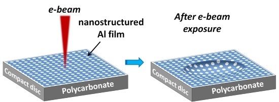
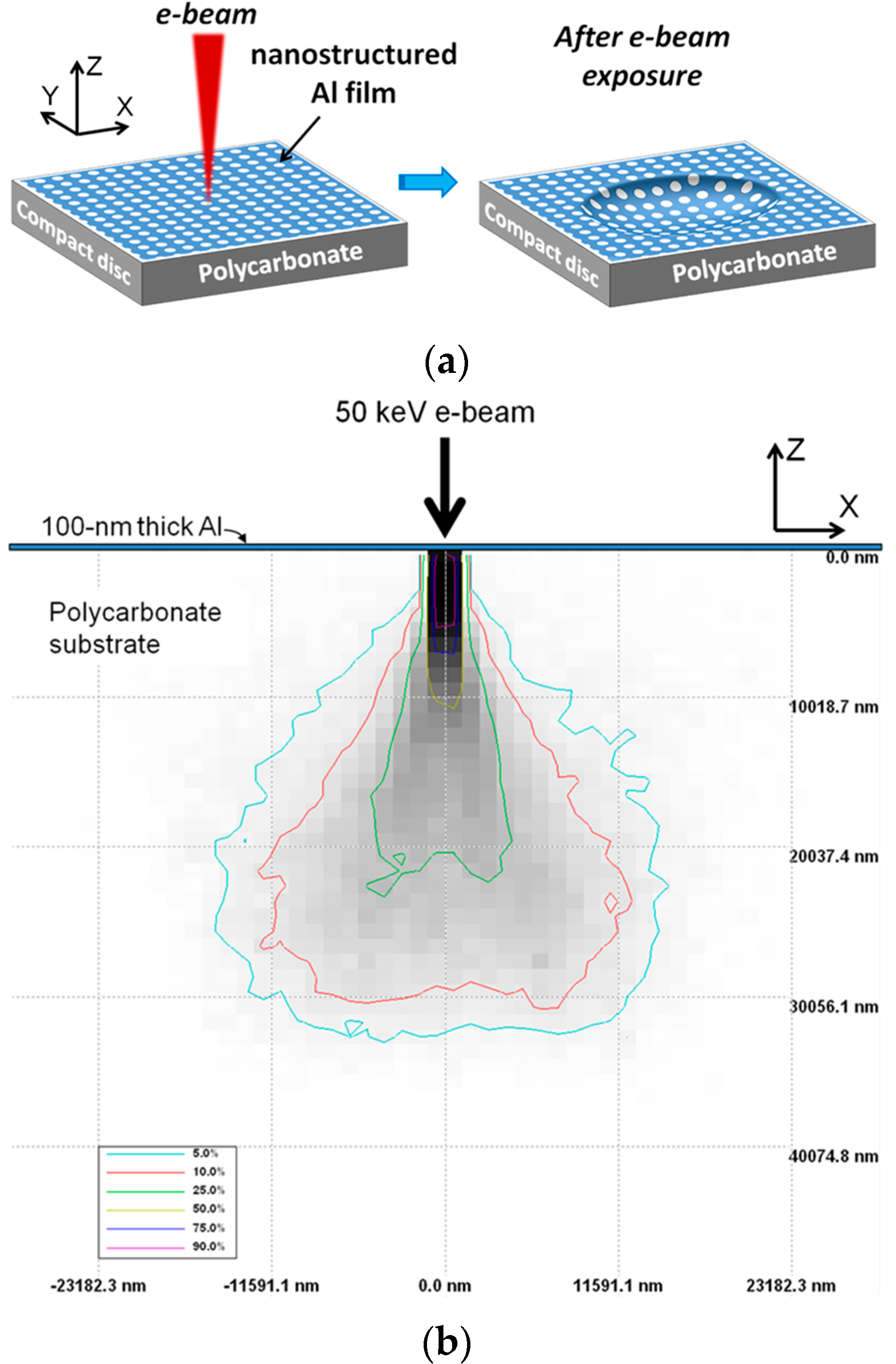
Here we introduce a non-contact approach to transform planar nanopatterned thin films on PC CDs into curvilinear geometries. In particular, we demonstrate that nanohole arrays (NHAs) drilled in Al thin films on PC CD substrates can be shaped by direct e-beam irradiation of the metal film surface. The method is schematically illustrated in
Figure 1. It is based on the penetration of incident electrons into the PC substrate where their energy is absorbed. This leads to crosslinking of the irradiated polymer region [
11] with consequent PC volume shrinking and film/surface deformation. The film curvature dependence on the main parameters of the shaping procedure is studied. As an example of application, we have fabricated a two-dimensional (2D) array of micro-lenses/reservoirs integrating a 2D NHA drilled in an Al film. Finally, we also demonstrate that the resulting non-planar nanopatterned metal surfaces on PC CD substrates can be easily transferred onto a flexible sticky tape by a simple
stick-and-peel process developed recently [
12].
2. Materials and Methods
2.1. Aluminum Nanohole Array Fabrication on PC CD Substrates
PC square substrates (12 mm × 12 mm) were cut from a 1.2-mm-thick standard CD (MPO Iberica, Madrid, Spain) using a dicing saw machine. The PC substrates were washed with detergent in ultrasonic bath, rinsed in deionized water (DIW) and isopropyl alcohol (IPA) and dried with N
2 flow. Then, an e-beam-evaporated 100-nm-thick layer of Al was deposited on the flat surface (
i.e., with no track) of the PC CD substrates. Next, ZEP-520 positive-tone e-beam lithography (EBL) resist was spin-coated on the Al films at 5000 rpm. The samples were then immediately baked for 10 min at 120 °C. Dot matrix arrays of pitches 500 nm and 635 nm were patterned in the resist film by using a Crestec CABL-9000 C high-resolution EBL system (acceleration voltage = 50 kV, beam current = 1 nA). The exposed resist was developed at 0 °C for 40 s and N
2 dried. Inductively coupled plasma (ICP) chemical dry etching was used to drill holes in the Al layer down to the PC substrate using the patterned ZEP-520 film as a mask. The ICP process was achieved using BCl
3 (20 sccm) and Cl
2 (10 sccm) gases and RF and ICP powers of 100 W. Immediately after the ICP etch, the samples were rinsed in DIW for 5 min to dissolve residual chloride ions. Finally, O
2 plasma treatment was carried out to remove resist residues and passivate the Al surface [
7].
2.2. Creation of Non-Planar Nanopatterned Al Surfaces on PC CD Substrates
The PC CD substrates containing the nanopatterned Al films were then subjected to direct e-beam irradiation of the metal films using the aforementioned EBL equipment (Crestec Corp., Tokyo, Japan) as shown schematically in
Figure 1a. Circles of diameters (
dinc) 2, 5 and 10 μm were written (scanned) with EBL at doses ranging from 12.8 to 320 mC/cm
2.
2.3. Transfer Printing onto a Flexible Support
The PC CD substrates containing non-planar nanopatterned Al films were fixed on a glass slide by gluing the back side of the PC substrate to the glass with cyanocrylate-based glue (Loctite, Henkel Corp., Westlake, OH, USA). A general purpose transparent PSA tape (#550 Scotch®, 3M, St. Paul, MN, USA) was used for pattern transfer. A 19-mm-wide by approximately 4-cm-long piece of tape was applied onto the nanopatterned Al surface on PC using finger pressure for approximately 1 min. Then the adhesive tape was peeled off manually to transfer the non-planar metal film from the PC substrate onto the tape.
2.4. Optical Transmission Spectra Measurements
The transmission spectra of the Al NHAs on PC were measured at room temperature with a Jasco V-650 UV–VIS spectrophotometer (Jasco Analytical Instruments, Easton, MD, USA) with nonpolarized light under normal incidence in the 500–700 nm wavelength range and a spectral resolution of 0.2 nm.
2.5. Surface Characterization
Surface morphology was characterized by a FEI Inspect F50 scanning electron microscope (SEM) (FEI, Hillsboro, OR, USA), an Alpha-Step IQ mechanical profiler (KLA-Tencor Corp., Milpitas, CA, USA) and an Ambios Xi-100 3D interferometric optical profiler (LOT-QuantumDesign Ltd., Surrey, UK).
3. Results and Discussion
Figure 1b displays the cross-sectional distribution of the absorbed energy in the PC CD substrate calculated with a Monte Carlo simulation software (Université de Sherbrooke, Sherbrooke, QC, Canada) [
13] for a 50 keV 10-nm-radius incident e-beam. The graph reveals that the electrons that cross the Al film and penetrate into the PC substrate are highly collimated up to a depth penetration of ~6 μm (dark region). As the electrons penetrate further they spread out, diminishing the absorbed energy density (light grey regions). PC crosslinking due to electron energy absorption should mostly take place in the dark area shown in
Figure 1b. The resulting volume shrinkage of the crosslinked region ought to produce an inward bending of the PC surface—and, therefore, of the uplying Al film—around the directly irradiated region.
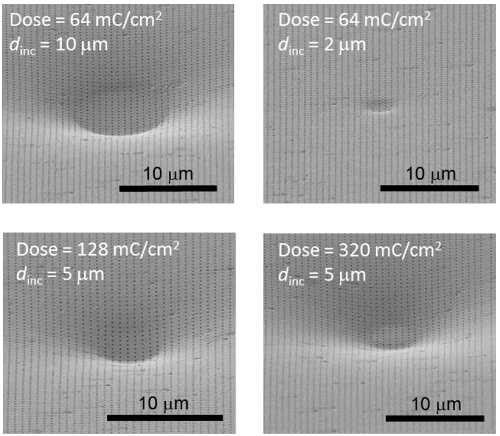
This is corroborated in
Figure 2, which shows SEM images of a 635-nm-period Al NHA film on a PC CD substrate on which circles with different
dinc values have been written directly by e-beam at several doses. It is seen that, after e-beam exposure, the patterned Al film is curved inwards, the directly irradiated circle being in the center of the circular depression. SEM analysis also revealed a uniform (un-cracked) curved Al NHA film for the studied EBL conditions.
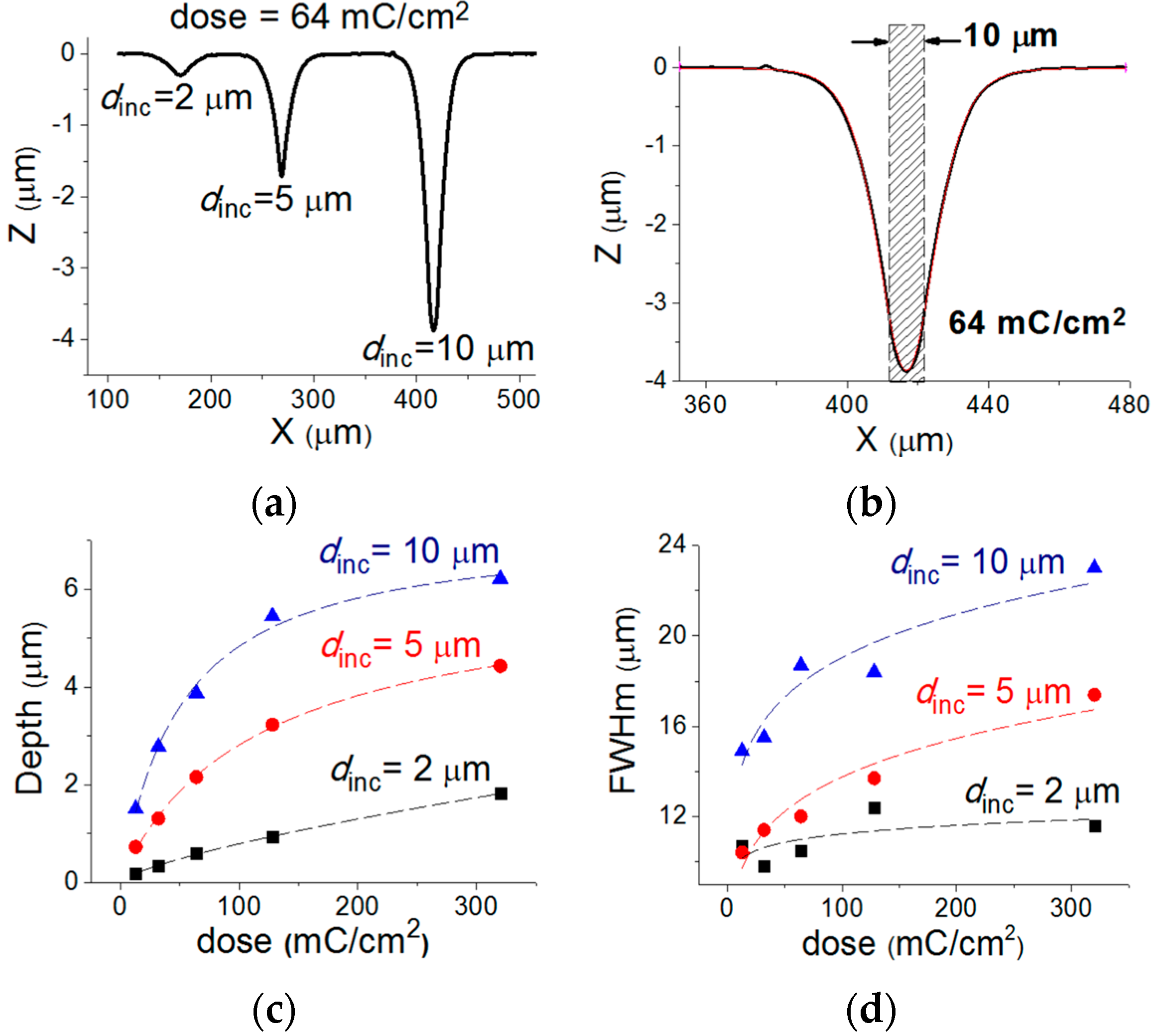
The profile along the diameter of the three dips created in the Al NHA/PC sample by e-beam irradiation at a dose of 64 mC/cm
2 and different irradiated diameters (
dinc = 2, 5 and 10 μm) is shown in
Figure 3a.
Figure 3b depicts the profile for
dinc = 10 μm as a representative case. The profile shape can be well fitted to a symmetric double sigmoidal function (red line in
Figure 3b: adjusted
R2 = 0.999).
Figure 3c,d plot the measured depth and full width at half minimum (FWHm) of the dips as a function of the electron dose for the three considered
dinc values. Both, depth and FWHm increase with both, the dose and
dinc. This is expected since an increment of dose and/or
dinc boosts the amount of penetrated electrons and, therefore, the degree of PC crosslinking and surface deformation. The measurements in
Figure 3c,d fit characteristic sigmoidal dose functions that saturate at large values of the dose. Saturation occurs because the number of PC molecules capable of absorbing the energy of the penetrated electrons is limited and due to the volume shrinking limitations of the polymeric material. The calibration sigmoidal curves of
Figure 3c,d can be used to engineer the geometry and dimensions of a targeted curvilinear Al film by proper choice of the pattern layout (written circle diameter) and the electron dosage.
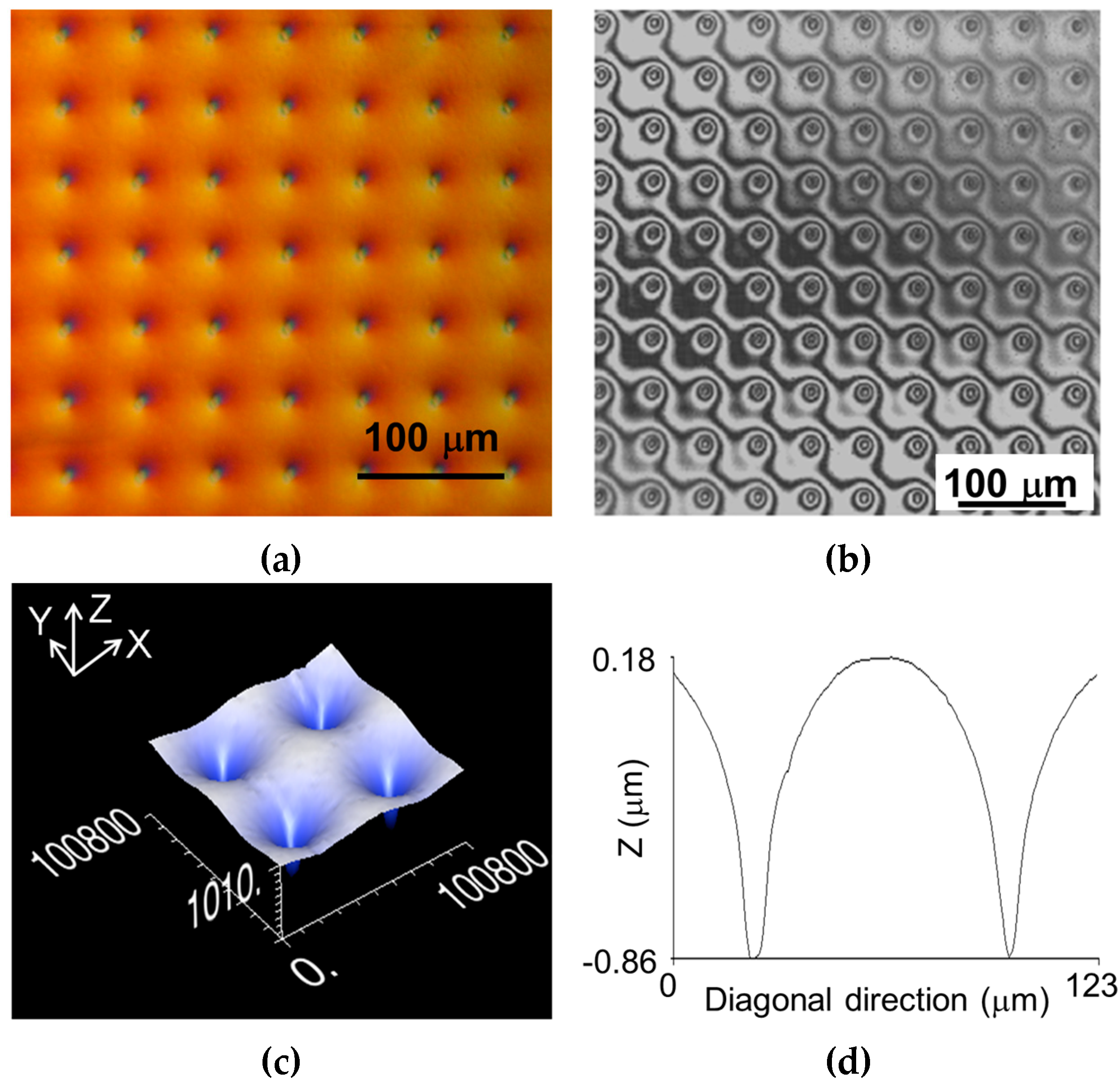
Figure 4a shows an optical microscope photograph of a 50-μm-period 2D array of circular dips created by e-beam irradiation (
dinc = 5 μm, dose = 32 mC/cm
2) of a 500-nm-period Al NHA on PC CD.
Figure 4b–d correspond to surface characterization by interferometric optical profiler. The dips exhibit clear concentric interference patterns (
Figure 4b) that are typical of curvilinear (concave and convex) circular surfaces. Note that the microdips can operate as both, diverging microlenses in transmission and converging micromirrors in reflection. The depth and width (FWHm) of the microlenses (
Figure 4c,d) were 1.04 and 11 μm, respectively. Note also that the surface among the dips is curved, but outwards, as a consequence of the neighboring dip proximity. This illustrates a method to create convex nanostructured film geometries using the presented e-beam irradiation procedure.
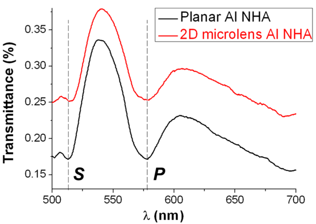
Figure 5 plots the spectral transmittance of the 500-nm-period Al NHA on PC-CD substrate before and after the creation of the microlenses. Both spectra exhibit similar spectral features. Minima denoted as
S and
P are attributed to the excitation of surface plasmon polaritons (SPPs) at the air-metal and substrate-metal interfaces, respectively [
7]. Thus, the 2D microlens array with the integrated NHA preserves the plasmonic effects due to the nanostructured Al film besides adding optical characteristics of diverging lenses. Note also that the dips can operate as micro-reservoirs for optical interrogation of small volumes of liquid samples, which makes this configuration suitable for implementing CD-based microfluidic microarrays for multiplex analysis of biomolecules.
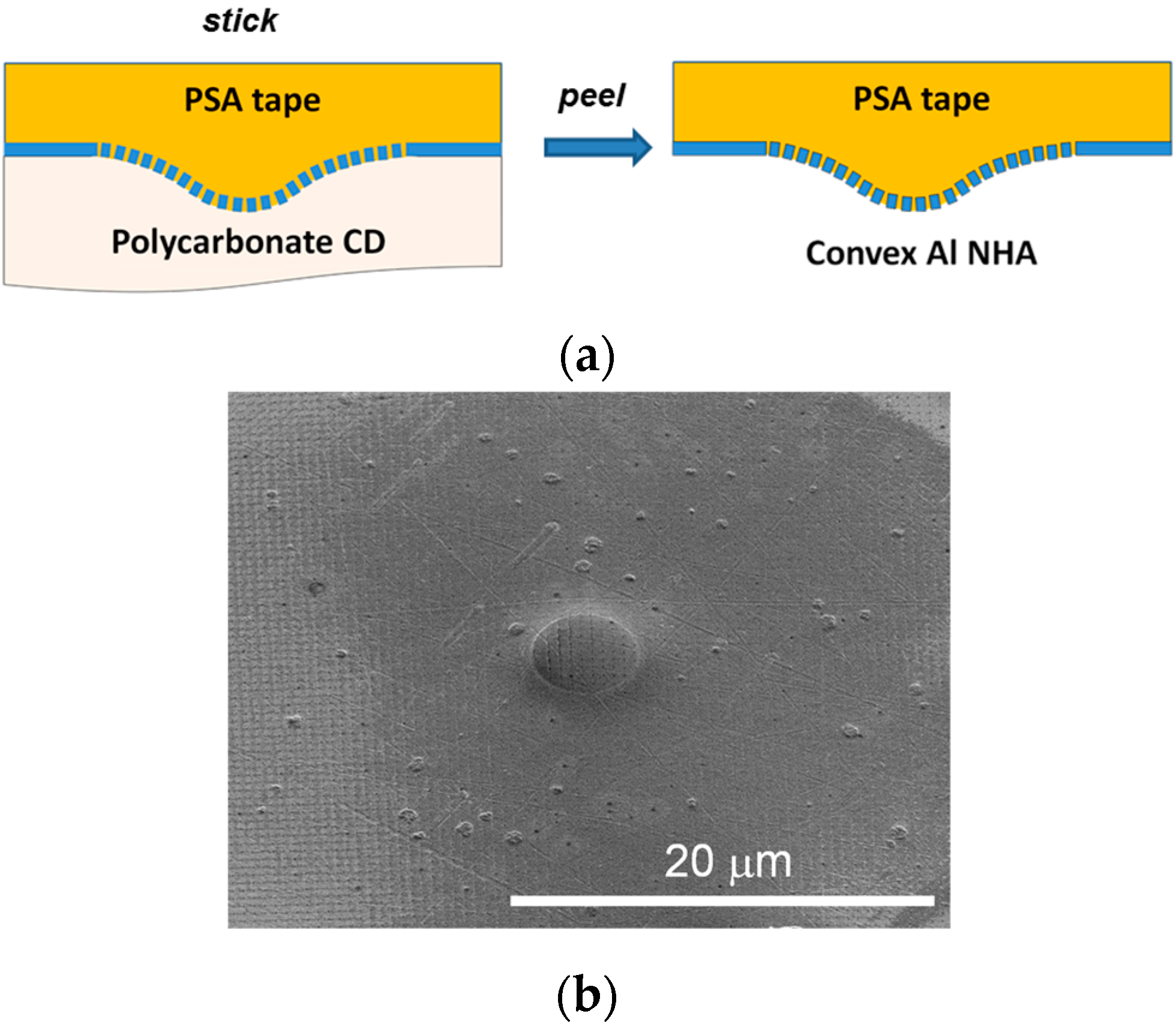
The 500-nm-pitch Al NHA curved film covering the 2D microlens array on PC CD substrate was also successfully transferred onto a Scotch tape by a
stick-and-peel procedure [
12], illustrated schematically in
Figure 6a. This produced convex (outward curved) nanopatterned Al film structures, as seen in the SEM photograph of
Figure 6b. Good film uniformity over a large area is observed (surface grooves and other surface inhomogeneities are attributed to the original CD surface from which the Al film was detached). The flexibility of the Scotch tape support increases the versatility of the structure, adding further curving and adhesive functionalities to the already curvilinear nanopatterned Al film.
4. Discussion
It should be noted that the film/surface shaping technology demonstrated here is suitable to be applied to a variety of thin film materials. In addition to Al, other metals (e.g., Au, Ti, Cr, Ni) can be deposited onto PC CD substrates by well-known deposition methods as thin films that allow 50 keV incident electrons to penetrate into the PC material. Similarly, besides PC, other polymeric materials prone to crosslinking under electron irradiation and capable of hosting thin films (e.g., poly(methylmethacrylate) [
14]) could be used as substrates. The use of PC CD is particularly remarkable because it is a highly available, ready-to-use, versatile and cost-effective material support.
For a given e-beam energy, the shaping limitations of the proposed method are determined by a variety of material and geometrical issues. Chemical composition and molecular structure of the substrate affect the penetration and absorbed energy of the incident e-beam and the maximum volume shrinkage (crosslinking) achievable in the irradiated polymer region. The film material composition and thickness also influence the penetration range and depth of the e-beam into the substrate. Even if the highest volume shrinkage is obtained, film-substrate adhesion strength, substrate elastic modulus and stiffness and pattern geometry of the deposited film impose a limit to the maximum surface/film curvature. Therefore, all these factors should be taken into consideration when selecting both, substrate and film materials for a particular application.
Finally, it should be mentioned that, although the conventional single-EBL direct-write system used in this work is not suitable for mass production due to its slow writing speed capacities, recent advances in the development of massively parallel electron beam direct-write (MPEBDW) systems [
15] are expected to address this roadblock.


