
In-Situ Testing of the Thermal Diffusivity of Polysilicon Thin Films


Abstract
:
1. Introduction
2. Theory
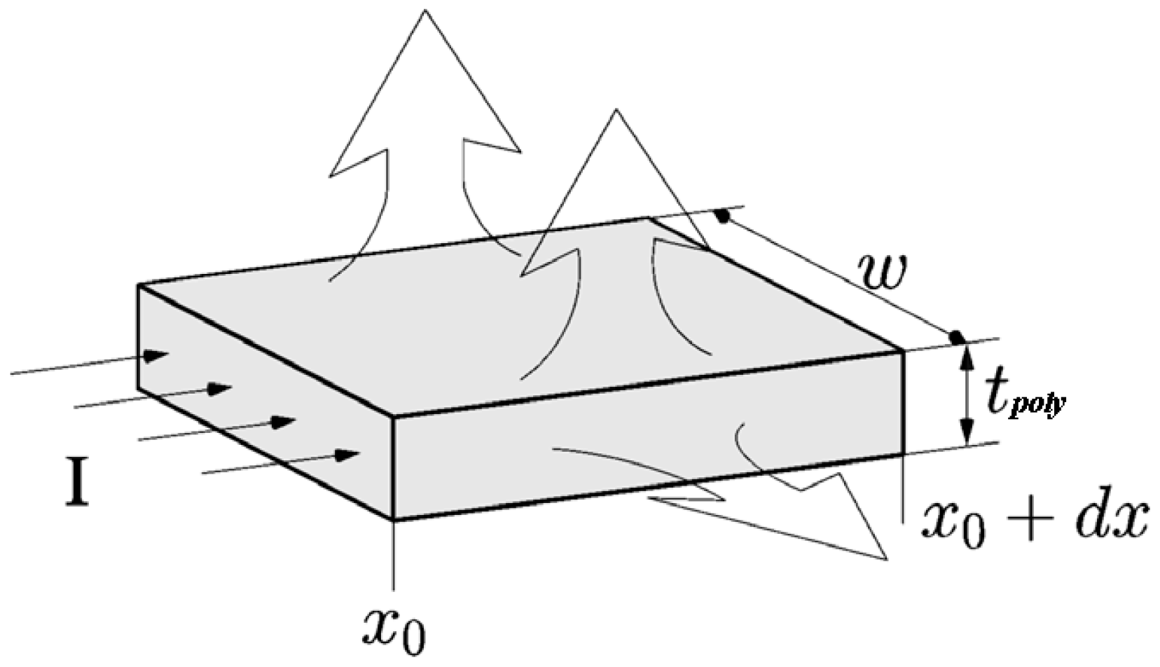
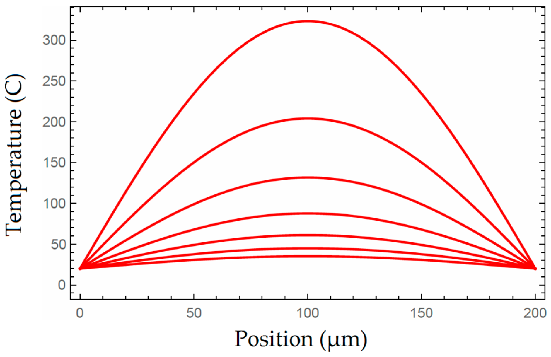
2.1. Heat Transfer
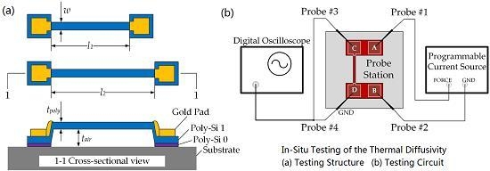
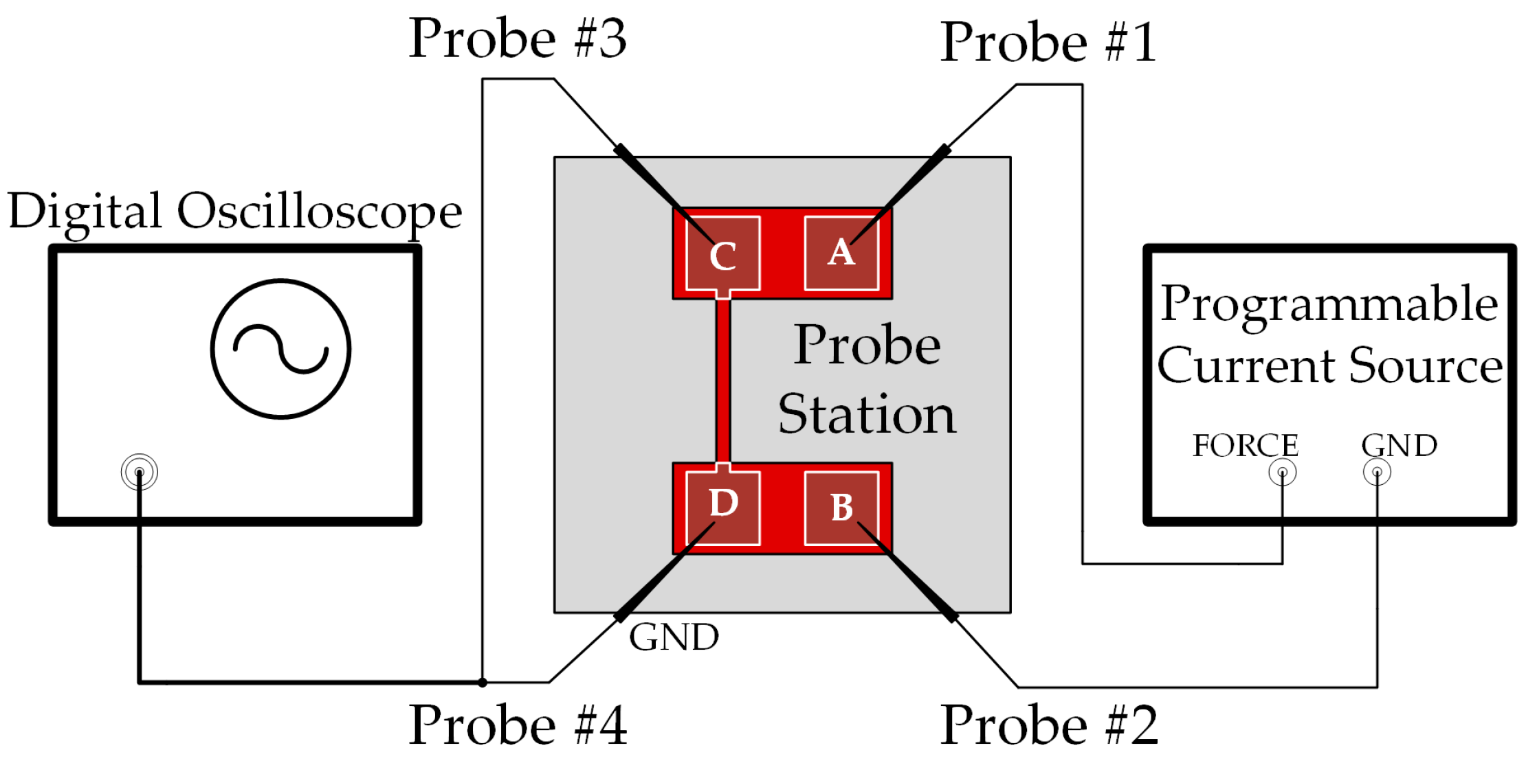
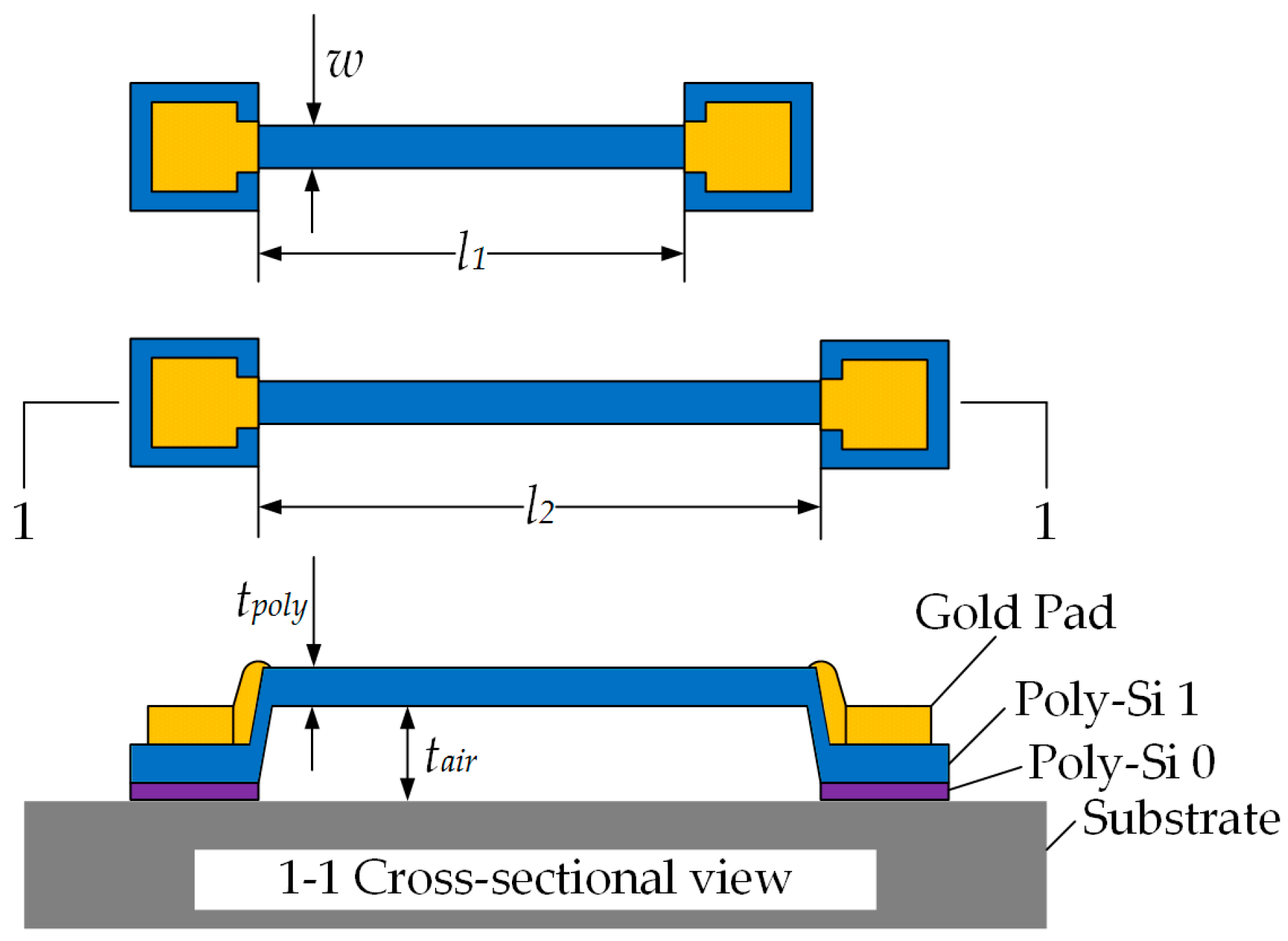
2.2. In-Situ Testing Structure and Thermodynamic Analysis
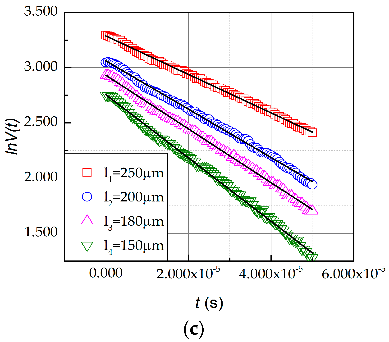
3. Experiment and Results
3.1. Fabrication
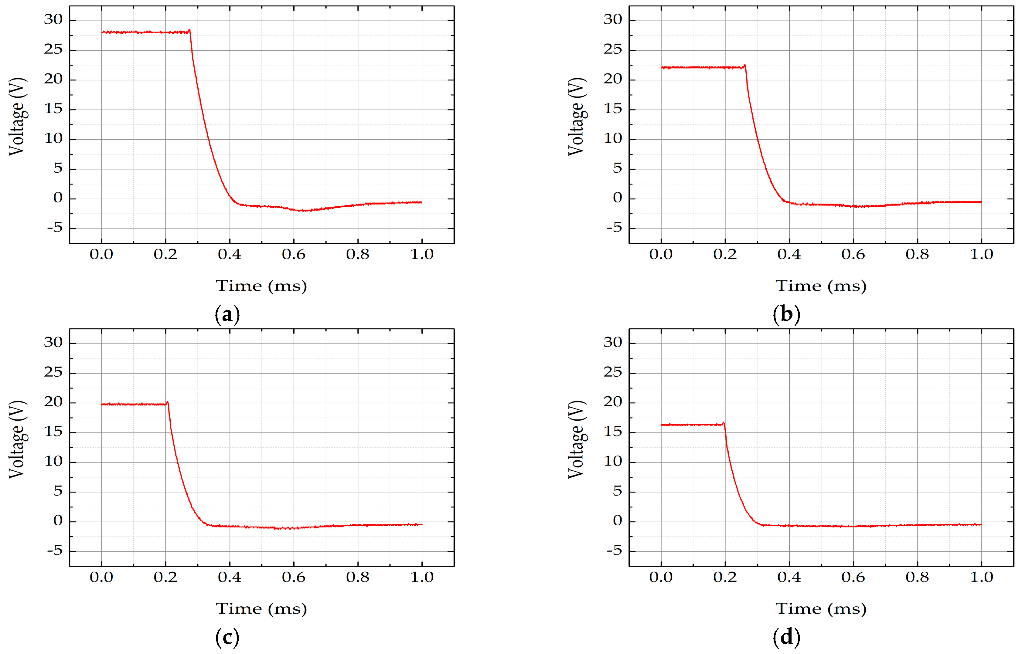
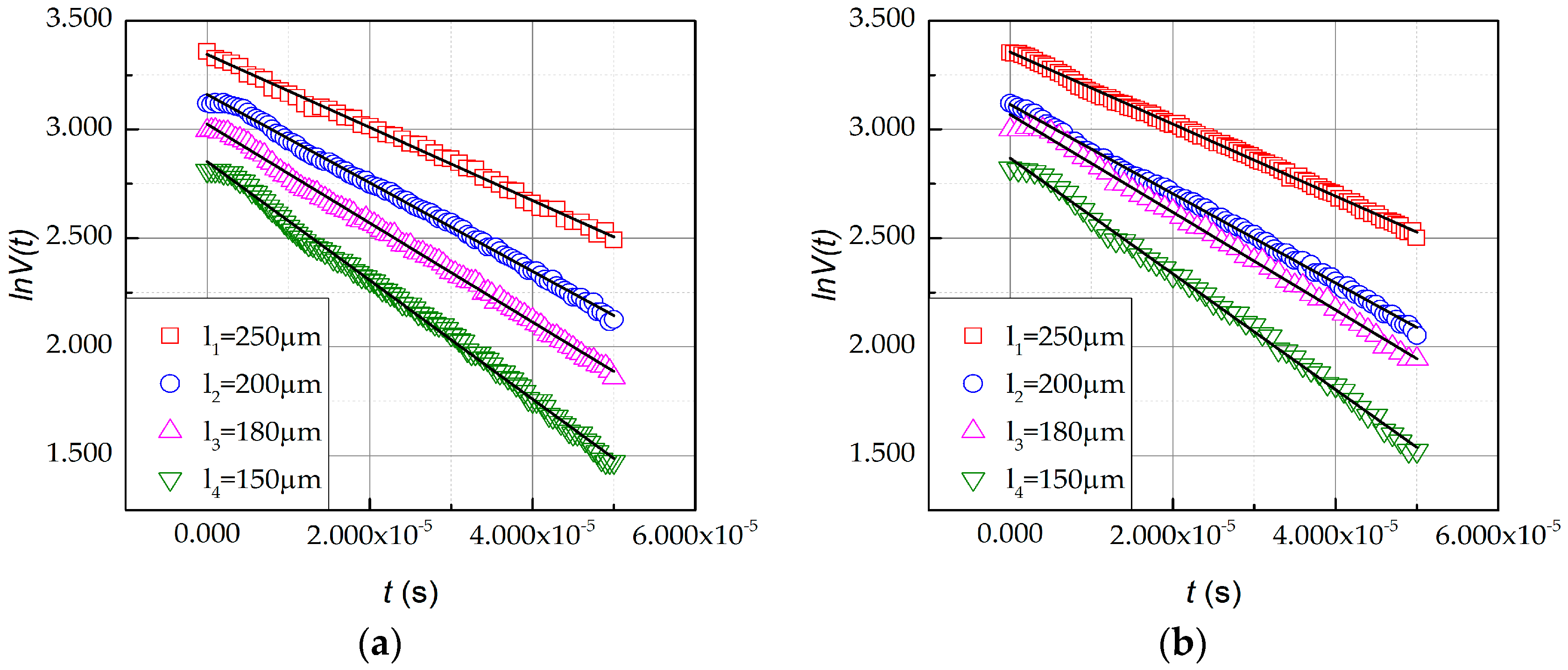
3.2. Experiment
3.3. Results
4. Conclusions
Acknowledgments
Author Contributions
Conflicts of Interest
References
- Chen, G.; Tien, C.; Wu, X.; Smith, J. Thermal diffusivity measurement of GaAs/AlGaAs thin-film structures. J. Heat Transf. 1994, 116, 325–331. [Google Scholar] [CrossRef]
- Cahill, D.G.; Katiyar, M.; Abelson, J. Thermal conductivity of α-Si: H thin films. Phys. Rev. B 1994, 50, 6077. [Google Scholar] [CrossRef]
- Völklein, F. Thermal conductivity and diffusivity of a thin film SiO2/Si3N4 sandwich system. Thin Solid Films 1990, 188, 27–33. [Google Scholar] [CrossRef]
- Irace, A.; Sarro, P.M. Measurement of thermal conductivity and diffusivity of single and multilayer membranes. Sens. Actuators A Phys. 1999, 76, 323–328. [Google Scholar] [CrossRef]
- Hatta, I.; Sasuga, Y.; Kato, R.; Maesono, A. Thermal diffusivity measurement of thin films by means of an AC calorimetric method. Rev. Sci. Instrum. 1985, 56, 1643–1647. [Google Scholar] [CrossRef]
- Grilli, M.; Aumann, T.; Ristau, D.; Dieckmann, M.; von Alvensleben, F.; Masetti, E. Thermal conductivity of e-beam and IBS coatings. In Optical Instrumentation & Systems Design; International Society for Optics and Photonics: Glasgow, UK, 1996; pp. 409–421. [Google Scholar]
- Parker, W.; Jenkins, R.; Butler, C.; Abbott, G. Flash method of determining thermal diffusivity, heat capacity, and thermal conductivity. J. Appl. Phys. 1961, 32, 1679–1684. [Google Scholar] [CrossRef]
- Zhang, X.; Grigoropoulos, C.P. Thermal conductivity and diffusivity of free-standing silicon nitride thin films. Rev. Sci. Instrum. 1995, 66, 1115–1120. [Google Scholar] [CrossRef]
- Moran, M.J.; Shapiro, H.N.; Boettner, D.D.; Bailey, M.B. Fundamentals of Engineering Thermodynamics; John Wiley & Sons: New York, NY, USA, 2010. [Google Scholar]
- Abedrabbo, S.M. Emissivity Measurements and Modeling of Silicon Related Materials and Structures. Ph.D. Thesis, New Jersey Institute of Technology, Newark, NJ, USA, 1998. [Google Scholar]
- Nishi, Y.; Doering, R. Handbook of Semiconductor Manufacturing Technology; CRC Press: Dallas, TX, USA, 2000. [Google Scholar]
- Dai, Z.; Xu, L.; Duan, G.; Li, T.; Zhang, H.; Li, Y.; Wang, Y.; Wang, Y.; Cai, W. Fast-response, sensitivitive and low-powered chemosensors by fusing nanostructured porous thin film and ides-microheater chip. Sci. Rep. 2013, 3, 1669. [Google Scholar] [CrossRef] [PubMed]
- Zhou, Q.; Sussman, A.; Chang, J.; Dong, J.; Zettl, A.; Mickelson, W. Fast response integrated MEMS microheaters for ultra low power gas detection. Sens. Actuators A Phys. 2015, 223, 67–75. [Google Scholar] [CrossRef]
- Garcia, D.; Leon, A.; Kumar, S. In-situ transmission electron microscope high temperature behavior in nanocrystalline platinum thin films. JOM 2016, 68, 109–115. [Google Scholar] [CrossRef]
- Phan, H.-P.; Dinh, T.; Kozeki, T.; Qamar, A.; Namazu, T.; Dimitrijev, S.; Nguyen, N.-T.; Dao, D.V. Piezoresistive effect in p-type 3C-SiC at high temperatures characterized using joule heating. Sci. Rep. 2016, 6, 28499. [Google Scholar] [CrossRef] [PubMed]
- Sun, Y.-C.; Liang, K.-C.; Cheng, C.-L.; Fang, W. A CMOS MEMS pirani vacuum gauge with complementary bump heat sink and cavity heater. In Proceedings of the 2014 IEEE 27th International Conference on Micro Electro Mechanical Systems (MEMS), San Francisco, CA, USA, 26–30 January 2014; pp. 676–679.
- Wang, G.-L.; Yang, D.-W.; Wang, Y.; Niu, D.; Zhao, X.-L.; Ding, G.-F. Heat transfer and friction characteristics of the microfluidic heat sink with variously-shaped ribs for chip cooling. Sensors 2015, 15, 9547–9562. [Google Scholar] [CrossRef] [PubMed]
- Nguyen, N.Q.; Pochiraju, K.V. Behavior of thermoelectric generators exposed to transient heat sources. Appl. Therm. Eng. 2013, 51, 1–9. [Google Scholar] [CrossRef]
- Rahman, Z.; Khir, M.M.; Burhanudin, Z. CMOS-MEMS thermoelectric generator for low power medical devices. In Proceedings of the 2015 IEEE Regional Symposium on Micro and Nanoelectronics (RSM), Langkawi, Malaysia, 19–21 August 2015; pp. 1–4.
- Lin, L.; Chiao, M. Electrothermal responses of lineshape microstructures. Sens. Actuators A Phys. 1996, 55, 35–41. [Google Scholar] [CrossRef]
- Fedder, G.K.; Howe, R.T. Thermal Assembly of Polysilicon Microstructures. Available online: https://www.ece.cmu.edu/~mems/pubs/pdfs/ieee/mems/0142_fedder-1991.pdf (accessed on 22 September 2016).
- Tai, Y.; Mastrangelo, C.H.; Muller, R. Thermal conductivity of heavily doped low-pressure chemical vapor deposited polycrystalline silicon films. J. Appl. Phys. 1988, 63, 1442–1447. [Google Scholar] [CrossRef]
- Acciani, G.; Falcone, O.; Vergura, S. Analysis of the thermal heating of poly-Si and a-Si photovoltaic cell by means of fem. Cell 2010, 4, 4. [Google Scholar]
- Bechtold, T.; Schrag, G.; Feng, L.; Hierold, C. System-Level Modeling of MEMS; Wiley-VCH: Weinheim, Germany, 2012. [Google Scholar]
- Geisberger, A.A.; Sarkar, N.; Ellis, M.; Skidmore, G.D. Electrothermal properties and modeling of polysilicon microthermal actuators. J. Microelectromech. Syst. 2003, 12, 513–523. [Google Scholar] [CrossRef]
- McConnell, A.D.; Uma, S.; Goodson, K.E. Thermal conductivity of doped polysilicon layers. J. Microelectromech. Syst. 2001, 10, 360–369. [Google Scholar] [CrossRef]
- Uma, S.; McConnell, A.; Asheghi, M.; Kurabayashi, K.; Goodson, K. Temperature-dependent thermal conductivity of undoped polycrystalline silicon layers. Int. J. Thermophys. 2001, 22, 605–616. [Google Scholar] [CrossRef]
- Nishimura, K.; Wang, H.; Fukunaga, T.; Kurata, K.; Takamatsu, H. Measurement of in-plane thermal and electrical conductivities of thin film using a micro-beam sensor: A feasibility study using gold film. Int. J. Heat Mass Transf. 2016, 95, 727–734. [Google Scholar] [CrossRef]
- Ftouni, H.; Blanc, C.; Sikora, A.; Richard, J.; Defoort, M.; Lulla, K.; Collin, E.; Bourgeois, O. Thermal Conductivity Measurement of Suspended Si-N Membranes from 10 K to 275 K Using the 3ω-Völklein Method. Available online: http://iopscience.iop.org/article/10.1088/1742-6596/395/1/012109/meta (accessed on 22 September 2016).
- Ma, W.; Zhang, X. Study of the thermal, electrical and thermoelectric properties of metallic nanofilms. Int. J. Heat Mass Transf. 2013, 58, 639–651. [Google Scholar] [CrossRef]
- Zhang, X.; Xie, H.; Fujii, M.; Takahashi, K.; Ikuta, T.; Ago, H.; Abe, H.; Shimizu, T. Experimental study on thermal characteristics of suspended platinum nanofilm sensors. Int. J. Heat Mass Transf. 2006, 49, 3879–3883. [Google Scholar] [CrossRef]


| Width w (μm) | Thickness tpoly 1 (μm) | Length l (μm) | Air GAP Thickness tair 1 (μm) | Sheet Resistance RS (Ω) | Young’s Modulus E (GPa) | Residual Stress σ (MPa) | |||
|---|---|---|---|---|---|---|---|---|---|
| 10 | 2 | l1 | l2 | l3 | l4 | 2 | 9.5 | 115.8 | −5.5 |
| 250 | 200 | 180 | 150 | ||||||
| Length l (μm) | Set #1 (s−1) | Set #2 (s−1) | Set #3 (s−1) |
|---|---|---|---|
| l1 = 250 | 1.721 × 10⁴ | 1.747 × 10⁴ | 1.741 × 10⁴ |
| l2 = 200 | 2.140 × 10⁴ | 2.150 × 10⁴ | 2.185 × 10⁴ |
| l3 = 180 | 2.424 × 10⁴ | 2.421 × 10⁴ | 2.431 × 10⁴ |
| l4 = 150 | 2.852 × 10⁴ | 2.846 × 10⁴ | 2.865 × 10⁴ |
| Thermal Diffusivity | Set #1 | Set #2 | Set #3 | Averaged Value |
|---|---|---|---|---|
| α (mm2/s) | 42.23 | 40.87 | 41.20 | 41.43 |
© 2016 by the authors. Licensee MDPI, Basel, Switzerland. This article is an open access article distributed under the terms and conditions of the Creative Commons Attribution (CC-BY) license ( http://creativecommons.org/licenses/by/4.0/).
Share and Cite
Gu, Y.-F.; Zhou, Z.-F.; Sun, C.; Li, W.-H.; Huang, Q.-A. In-Situ Testing of the Thermal Diffusivity of Polysilicon Thin Films. Micromachines 2016, 7, 174. https://doi.org/10.3390/mi7100174
Gu Y-F, Zhou Z-F, Sun C, Li W-H, Huang Q-A. In-Situ Testing of the Thermal Diffusivity of Polysilicon Thin Films. Micromachines. 2016; 7(10):174. https://doi.org/10.3390/mi7100174
Chicago/Turabian StyleGu, Yi-Fan, Zai-Fa Zhou, Chao Sun, Wei-Hua Li, and Qing-An Huang. 2016. "In-Situ Testing of the Thermal Diffusivity of Polysilicon Thin Films" Micromachines 7, no. 10: 174. https://doi.org/10.3390/mi7100174