Article

Fiber-Based, Injection-Molded Optofluidic Systems: Improvements in Assembly and Applications

by
Marco Matteucci
1,
Marco Triches
2,3,
Giovanni Nava
4,
Anders Kristensen
1,
Mark R. Pollard
2,*,
Kirstine Berg-Sørensen
5,* and
Rafael J. Taboryski
1,*
1
Department of Micro- and Nanotechnology, Technical University of Denmark, Ørsteds Plads, Building 345B, Kgs. Lyngby 2800, Denmark
2
DFM A/S Matematiktorvet 307, Kgs. Lyngby 2800, Denmark
3
Department of Photonics Engineering, Technical University of Denmark, Ørsteds Plads, Building 343, Kgs. Lyngby 2800, Denmark
4
Department of Medical Biotechnology and Translational Medicine, Università degli Studi di Milano, Milan 20122, Italy
5
Department of Physics, Technical University of Denmark, Fysikvej, Building 309, Kgs. Lyngby 2800, Denmark
*
Authors to whom correspondence should be addressed.
Micromachines 2015, 6(12), 1971-1983; https://doi.org/10.3390/mi6121468
Submission received: 7 November 2015 / Revised: 1 December 2015 / Accepted: 4 December 2015 / Published: 9 December 2015
(This article belongs to the Special Issue Optofluidics 2015)

Abstract

:
We present a method to fabricate polymer optofluidic systems by means of injection molding that allow the insertion of standard optical fibers. The chip fabrication and assembly methods produce large numbers of robust optofluidic systems that can be easily assembled and disposed of, yet allow precise optical alignment and improve delivery of optical power. Using a multi-level chip fabrication process, complex channel designs with extremely vertical sidewalls, and dimensions that range from few tens of nanometers to hundreds of microns can be obtained. The technology has been used to align optical fibers in a quick and precise manner, with a lateral alignment accuracy of 2.7 ± 1.8 μm. We report the production, assembly methods, and the characterization of the resulting injection-molded chips for Lab-on-Chip (LoC) applications. We demonstrate the versatility of this technology by carrying out two types of experiments that benefit from the improved optical system: optical stretching of red blood cells (RBCs) and Raman spectroscopy of a solution loaded into a hollow core fiber. The advantages offered by the presented technology are intended to encourage the use of LoC technology for commercialization and educational purposes.

Graphical Abstract

1. Introduction

Since 2005 [1] merging of optics and fluidics at the micro and nanoscale for Lab-on-Chip (LoC) purposes opened a wide range of opportunities both in basic and applied research [2]. Despite many demonstrations of technical feasibility and the continued broadening of the field, few devices with optical functionalities have reached the market. The limited commercialization of this technology lies in the fact that, at present, the majority of LoC optofluidic systems are fabricated with techniques that are not production-friendly either in terms of materials or in terms of optical elements: Existing microfluidic systems in glass are characterized by high production cost and, in addition, optofluidic systems with waveguides produced using femtosecond laser machining [3] or DUV writing [4] suffer from high optical losses. Alternatively, low-loss, optical fiber-based systems made in soft polymer materials like polydimethylsiloxane (PDMS) require more laborious procedures such as pneumatically driven active optical fiber manipulators [5] for optical alignment on-chip because of the fiber housing deformation. The ideal system would be easy to align with high precision, mechanically strong, easy to interface with both fluidics and optics, have negligible biofouling, deliver high power in situ and would be disposable.
To make a substantial improvement towards such systems, we developed injection molded (i.e., production-friendly) optofluidic chips in hard Cyclic Olefin Copolymer (CoC) TOPAS 5013 with embedded commercially available optical fibers (Figure 1a,b). We consider TOPAS 5013 to be an ideal polymer for fabrication of LoC systems because of its high transparency in the visible wavelength range [6], its high glass transition temperature (140 °C), its low water absorption and its resistance to acids and alkaline agents, as well as to polar solvents [7]. TOPAS also avoids undesired biofouling with minimal surface treatment requirements [8] and autofluorescence of TOPAS 5013 can be reduced to values that are about 20% lower than the ones of silica chips [9].
Figure 1. (a) Optofluidic chip in TOPAS 5013 L10 polymer with a system for hydrodynamic focusing of cells and embedded optical fibers. Optimal coupling with external fluidics is ensured by the presence of on-chip standard Luer connectors. The chip was designed with three inlet ports to allow hydrodynamic focusing of cells. (b) Detail of chip with a photonic crystal fiber (Left) and single-mode fiber (Right).
Micromachines 06 01468 g001
Compared to earlier demonstrations of optofluidic devices with embedded commercial optical fibers [10,11] the reported chip fabrication process is production ready and allows the height of the optical beam path relative to the microfluidic channel to be tuned easily in the design phase. Moreover, novel process modifications involving a double positive resist exposure (described in the “Materials and Methods”, Section 4.1) allowed the fabrication of the novel auto-aligning two-level square geometry for fiber housing. For our purposes, we embedded standard bare optical fibers with a nominal diameter of 125 μm and interfaced them with a microfluidic channel of 100 μm × 100 μm section (Figure 1b), thus producing an optical path at a height of around 40 μm above the channel surface. The dimensions of the fluidic channel were chosen to balance the requirements of hydrodynamic resistance and of delivery of the optical power to the center of the channel (for optical stretching). The chosen distances also proved to be a good compromise for delivery of power across the channel (for the Raman sensing). Uniquely, the fiber grooves have a square design ensuring reproducible alignment by constraining the lateral fiber movement. In general, any fiber with a diameter of 125 μm could be inserted in the chip described here, whereas other dimensions require a simple modification in the design phase. To validate the chip functionality and versatility, we present results obtained through the utilization of the chips for both optical stretching of red blood cells (RBCs) and for in-fiber Raman spectroscopy of liquids. Both techniques require a high level of alignment precision and coupling [12], for this reason they are considered ideal examples for the application and validation of the technology.

2. Results

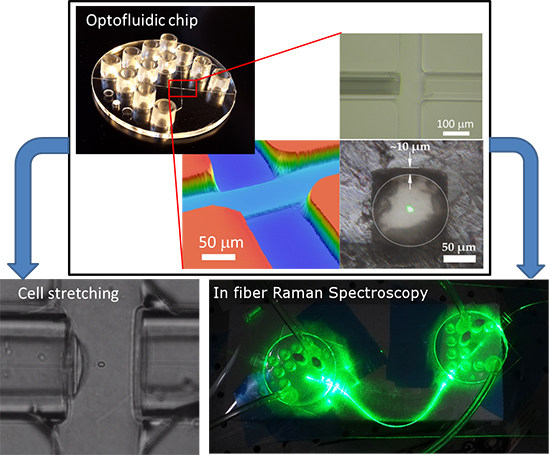
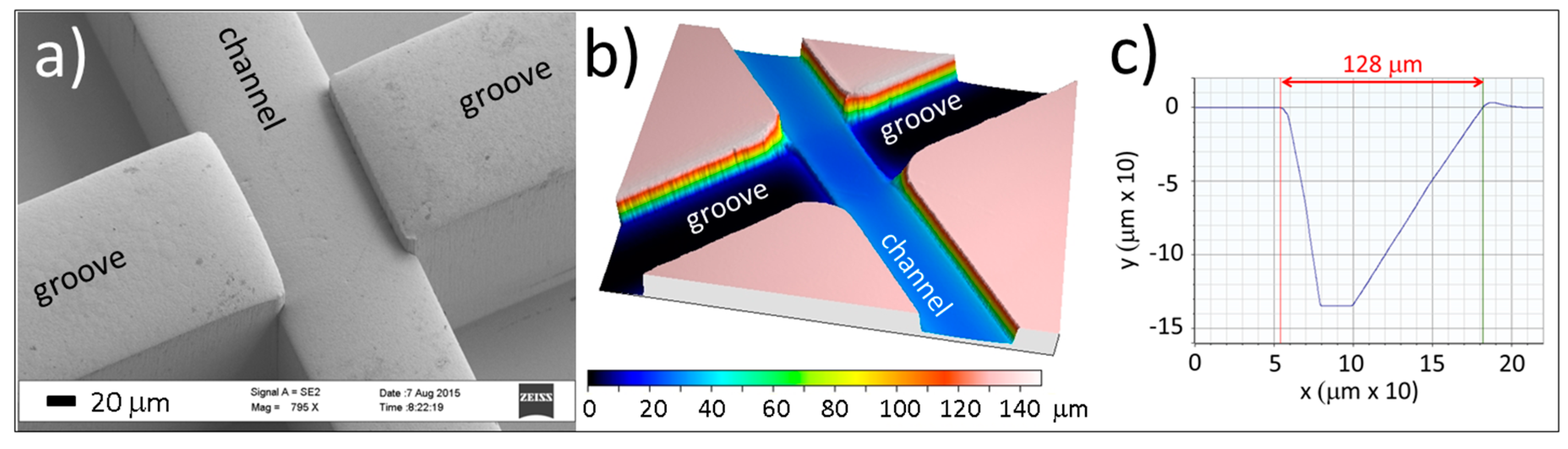
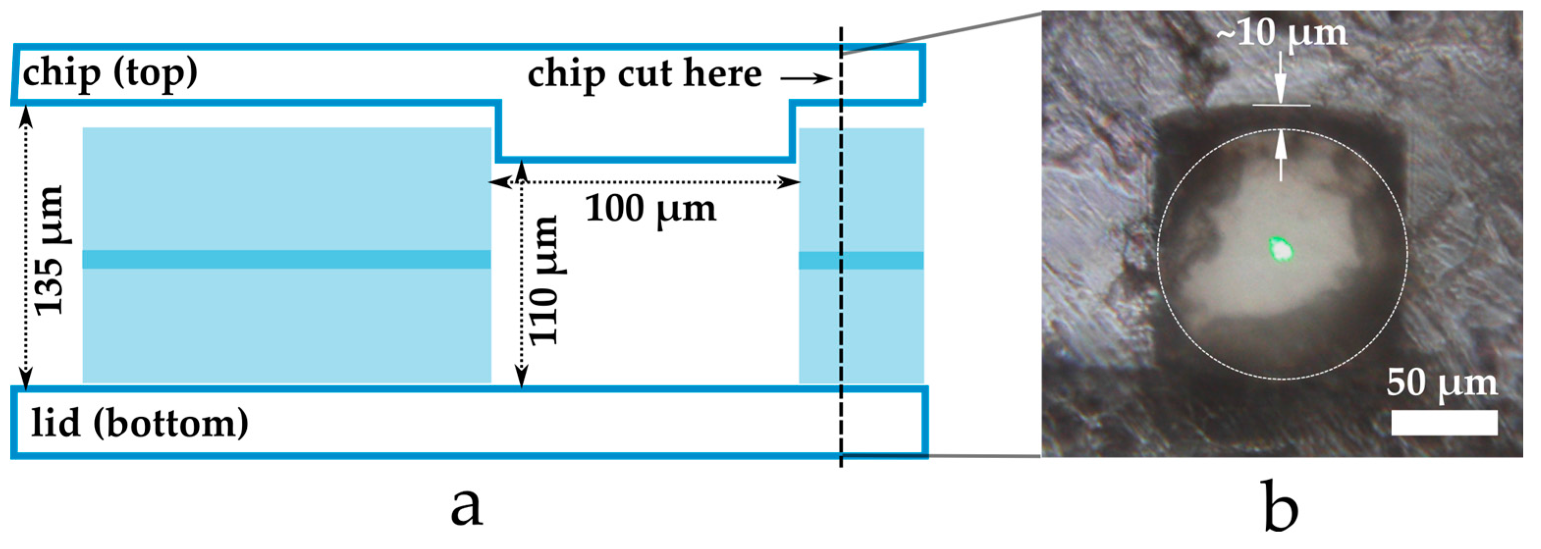
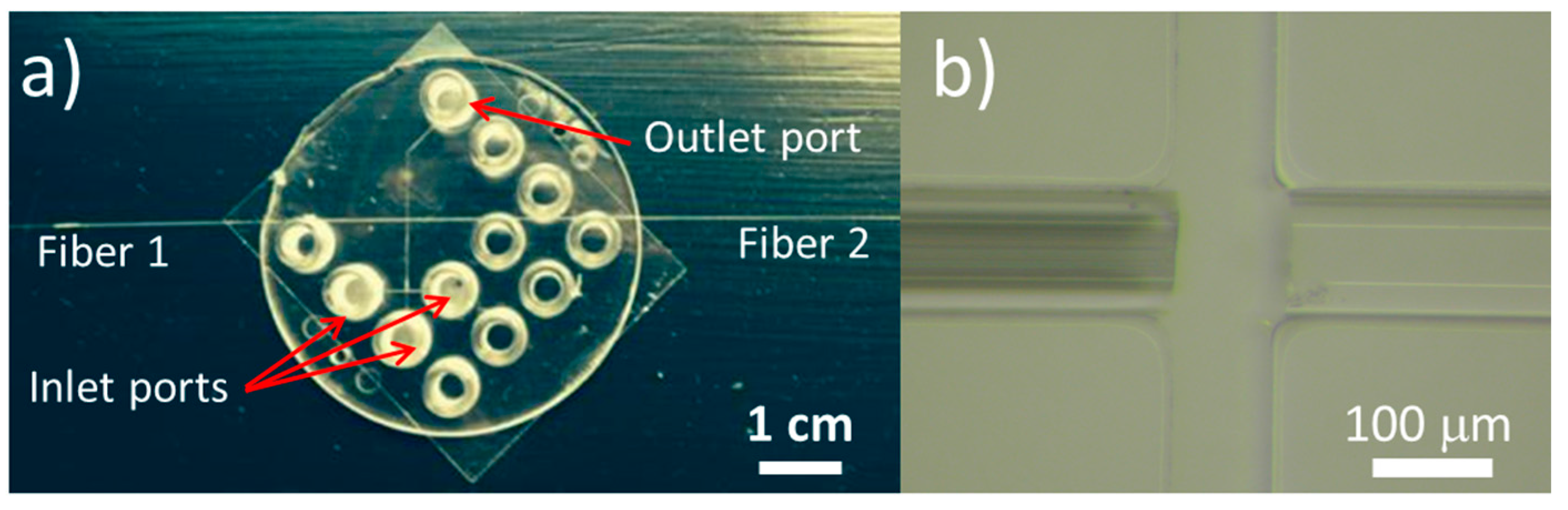
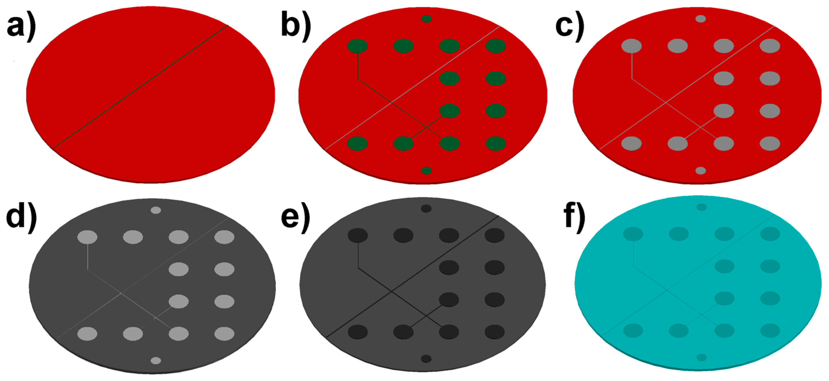
2.1. Fabrication Results

Figure 2 shows a scanning electron microscopy image (Figure 2a) of the Ni stamp (here referred to as shim) together with optical (Figure 2b) and mechanical (Figure 2c) profilometry data of the polymer chip. A groove width of 128 μm was measured by means of mechanical profilometry with an uncertainty of 2.5 µm, which is compatible with the designed width of the fiber groove (125 μm). In the final samples, while the difference in height between the fiber groove and the channel was measured to be around 25 μm (Figure 2b), the total depth of the groove of the final systems was around 135 μm (Figure 2b,c).
Figure 2. (a) SEM micrograph of the Ni shim in the area where the fiber grooves meet the channel; (b) Confocal microscope profilometry of the polymer chip that shows the channel depths and the difference between the groove and the channel; (c) Mechanical profilometry of the fiber grooves inside a polymer chip. NB, this is a convolution of groove dimensions and dimensions of the profilometer tip (5 μm in diameter).
Micromachines 06 01468 g002
In order to properly seal the fibers in the channels, a higher bonding temperature (130 °C instead of 125 °C) was chosen to allow controlled swelling of the polymer lid inside the fiber groove during bonding and the formation of a tight microfluidic seal. The effect of bonding the lid onto the optofluidic chip was observed by the cross-section of an assembled chip (which was assembled following the method reported in Section 4.1). In this case, the lid was a 2 mm thick 2-inch of TOPAS wafer and it was thermally bonded to the chip, which permitted cutting and polishing of the test sample. The assembled chip was cut in half using a jeweller’s saw, polished using diamond lapping paper (Thorlabs LF6D, Newton, NJ, USA) and finally observed using a microscope (Nikon, ×40 objective lens, Tokyo, Japan) as shown in Figure 3. Green laser light was coupled into one end of a single mode fiber and was observed at the other fiber end in the chip cross-section (see Section 2.3 for further details on the coupling of laser light into the fiber).
Figure 3. Effect of lid bonding on assembled chip: (a) Design of an assembled chip; (b) cross-section of assembled chip including single mode fiber fixed within the fiber groove, transmitting green laser light. The outline of the fiber has been enhanced to make it visible.
Micromachines 06 01468 g003
The image shows that the width (i.e., horizontal dimension in Figure 3b) of the groove fits well to the diameter of the fiber (125 µm), whereas the depth of the groove is approximately 10 µm greater than the fiber diameter. This gap was deliberately included in the chip design to accommodate swelling of the lid during its bonding to the chip, but can act as a cause of fiber misalignment.
Ten chips were assembled and the distance between the ends of the two cleaved fibers was measured for all chips using a microscope (Nikon, ×20 objective lens). The average distance between the ends of the two cleaved fibers is 104.6 with a maximum uncertainty of ±2.4 µm.
We tested the fiber alignment by checking the optical power transmitted through one unfilled chip (i.e., no fluid in between the fibers). The chip was assembled using two single-mode fibers (Thorlabs SM980), equipped with standard fiber connectors. A fiber laser emitting at 1550 nm wavelength was used to perform the test. The injected power was measured to be 15.19 mW, while the output was 8.03 mW. Using this information and neglecting the fiber loss (less than 0.001 dB/m at this wavelength as reported in the datasheet), we calculate the transmission across the empty junction to be 53%. Comparing this result with the theoretical loss expected in a fiber-to-fiber coupling (as described in Materials and Methods Section 4.3), we retrieve a lateral misalignment of 2.7 ± 1.8 µm. As shown in Figure 3b, we believe this fiber misalignment most likely occurs in a vertical direction.

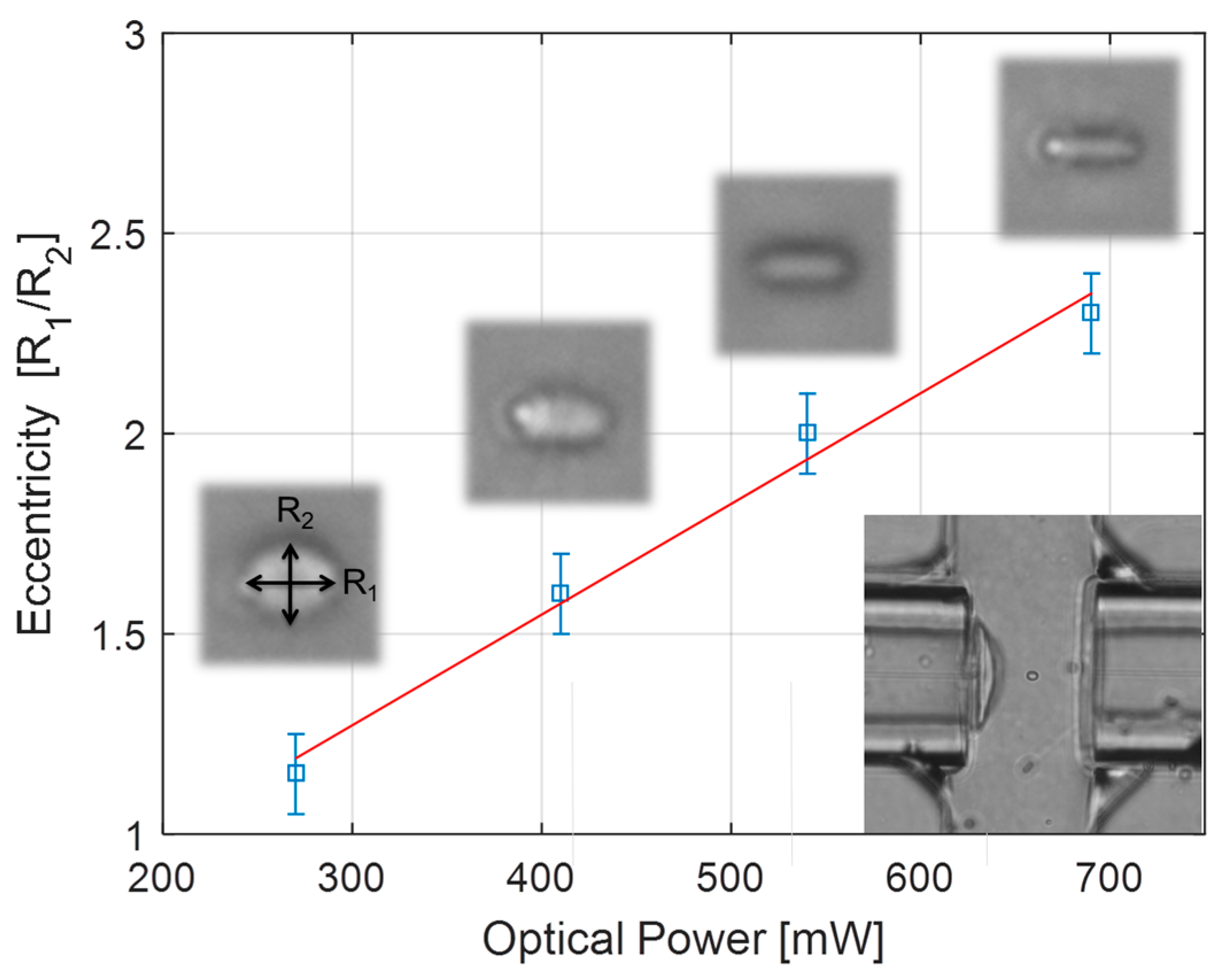
2.2. Single Chip Applied in Optical Stretching

Optical stretching [13] is highly relevant for the study of mechanical properties of single cells. Mechanical properties of cells have been shown to be closely related to the health of the studied biomaterial [14]. Here, for demonstration, we trapped and stretched single red blood cells (RBCs). The embedded single-mode (SM) fibers were connected to two independent diode lasers, we prefer the independent lasers as we may therefore easily tune the optical forces from each by varying the power of the two lasers. We took care to use two identical lasers to ensure similar time response. Both the laser powers and pump flow rates could be controlled using a custom made LabView code. To see the trapping region and recording the images of the trapped objects, the chip was mounted on an inverted microscope with a CCD camera. The RBCs were suspended in a hypotonic buffer solution with low osmotic pressure in order to obtain spherical RBCs of 8 µm diameter. The minimum power to trap the cells was found to be around 100 mW from each laser diode.
Once a cell was trapped, the laser power was increased in four to seven steps up to the maximum value (450 mW output from the laser), while returning to the minimum power between each step to allow the cell to relax. For each laser power, the images of the cell were recorded and both main and minor axes were measured. The ratios of the major and minor cell diameters were then determined using an image processing code and displayed as a function of the total laser power from two lasers (Figure 4). The data obtained reveals that the ratio between main and minor axes of RBC changes linearly with applied power in the power range used. As expected, the axial scattering forces, in the direction of propagation of the counter propagating beams, act to provide a stable trapping point in the axial direction and to stretch the cells (direction of R1) whereas the transversal force, due to the field gradient perpendicular to the optical axis (direction of R2), merely assists to capture and stably trap the cells in the transversal direction [15]. The results in Figure 4 are in good agreement with results obtained by Guck et al [16]. The simplicity of use was verified during the PolyNano summer school 2014 [17] where students with no previous experience could easily assemble the described chips and use them for cell stretching experiments with only two days of work. Four student groups produced four different chips, all with well aligned fibers, and trapped polystyrene beads and/or red blood cells in these chips.
Figure 4. Stretching of a single RBC. The stretching ratios, R1/R2 of a RBC in the optical stretcher as a function of total stretching laser power. The major and minor axes of the cell were measured using the corresponding images shown as insets. Resulting values and error bars are the result of edge-detection in 30 images recorded at the same laser power. In the lower right corner, the inset shows a black and white image of a red blood cell trapped between the two SM optical fibers embedded in the microfluidic chip.
Micromachines 06 01468 g004

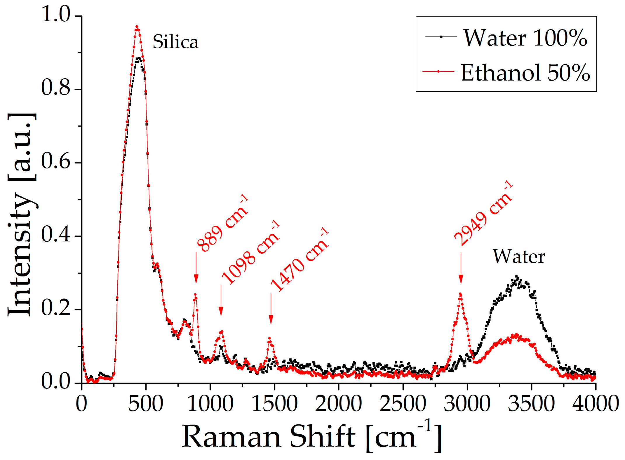
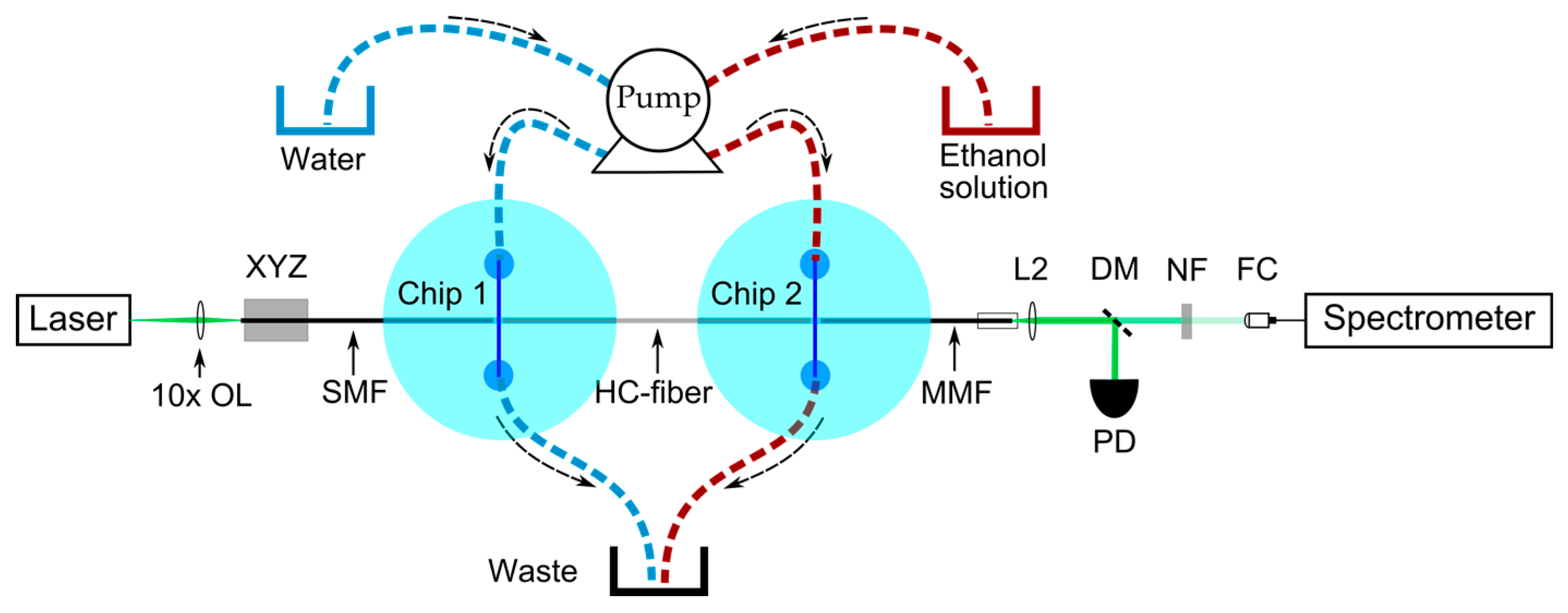
2.3. Dual Chip Applied in Fiber-Based Raman Spectroscopy

Our polymer chip technology was used to create a new experimental setup for the Raman spectroscopy of liquids. Our system was made by the quick and simple integration of a hollow core fiber (HC fiber) [18] between two chips, where the hollow core can be filled with different liquid samples by pumping liquid from alternate ends of the HC fiber, as described by Khetani et al. [8]. The system (including the HC fiber) was initially filled by pumping milli-Q water into Chip 1 at a rate of 230 µL/min (see Materials and Methods for experiment diagram). A transmission of 10% was achieved, and the Raman spectrum for the sample (Figure 5, black curve) showed the expected peaks created by Raman scattering from the water molecules loaded in the HC-fiber and the silica molecules present in all the optical fibers.
A transmission of 10% was achieved, and the Raman spectrum for the sample (Figure 5, black curve) showed the expected peaks created by Raman scattering from the water molecules loaded in the HC-fiber and the silica molecules present in all the optical fibers.
Figure 5. Raman spectra for solutions filled into hollow core fiber, showing ethanol solution (red) and milli-Q water (black).
Micromachines 06 01468 g005
Next, the HC fiber was refilled with an ethanol solution (50:50 water/ethanol by volume) which was flowed into Chip 2 using the same flow rate. The filling process was monitored by observing changes in the spectra, after 90 min the spectra did not vary further, indicating that filling was complete. This filling time given the calculated pressure difference across the HC fiber (17.2 kPa) agrees with previous work [8]. The pressure difference across the two chips is calculated based on the dimensions of the chip’s microfluidic channel and the microstructure of the HC-fiber. The viscosity of the ethanol solution was calculated using the Refutas equations [19]. The low pressure applied across the fiber was chosen to characterize the filling time. The overall filling time can be reduced by increasing the pressure thanks to the mechanical properties of the optofluidic system fabricated (more details in the Discussion, Section 3).
The resulting Raman spectrum contained additional signals from the ethanol solution (Figure 5, red curve) that agreed with reported spectra [20,21], and a reduction in the water peak due to dilution with ethanol was observed. All spectra are based on an average of five spectra recorded with an integration time of 2 s, with a three-point moving average applied to reduce spectrometer noise. For comparison purposes, the spectra were normalized using 30 data points that occurred across the broad Silica peak at 500 cm−1.

3. Discussion

The technology proposed demonstrates its versatility thanks to the two different optofluidic applications presented. The chip technology has such high repeatability that multiple chips can be concatenated together (as demonstrated in the Raman experiment). In order to balance between the requirements of hydrodynamic resistance and of delivery of the optical power, overlap of deep channels and removal of solid wall separation are required. This marks a difference with previous work [22,23]: in order to precisely overlap deep channels with slight difference in depth, a modified multilayer process is required. The reason is that once a deep channel is dry etched into silicon, the spin coating of a uniform layer of resist for an aligned UV exposure is not possible due to the resist entering the deep channel.
The square shape of the fiber grooves was chosen to reduce the volume surrounding the fiber (with respect to a V-shape), reducing possible leaking and improving the fiber gluing. Grooves with very sharp edges are obtained thanks to the extreme verticality of the DRIE process used. Additionally, the square shape combined with the asymmetric dimensions of the groove (125 µm width × 135 µm depth) allows to compensate the effect of the bonding onto the lid. The lid surface is expected to swell inside the channel/groove due to the force/temperature combination applied in the bonding procedure. The effect has been quantified on the order of 6–8 µm in previously unpublished work, using 100 µm thick lid. Although the bonding procedure developed works successfully with 100 µm and 2 mm thick lid, the effect may vary with the lid thickness. As reported in Figure 3, the 2 mm lid does not seem to suffer of this effect at the higher temperature applied.
All the chips tested were assembled by gluing the fiber in place and subsequently bonding the lid, but the chip design also allows the lid to bond in the first step and subsequently inject the fiber and glue it in place. The first procedure is easier to implement because it does not require special skills on the fiber handling, making it preferable for the didactic purposes of the chip design. The average distance between the ends of the two cleaved can be influenced by mechanical traction applied on the fiber when the glue is not completely cured and can be detrimental for the applications, because of the poor optical coupling in the fiber-to-fiber junction.
The second approach can solve this issue but the fiber insertion requires extreme caution to avoid possible damage of the fiber tip, which will compromise the optical properties of the system as well. For this reason, a novel mask design with a larger section of the groove at the fiber entrance is required. Additionally, the depth of the groove needs to be optimized to minimize the causes of misalignment. Bonding was performed with lids ranging in thicknesses from 100 μm to 2 mm before the insertion and gluing of the fibers. Not only did the placement of the fibers after chip sealing provide a simplified alternative assembly but the bonding of thicker lids makes it possible to have systems with resistance to higher pressures (up to 9 bar with a 100 μm lid) [23]. Thanks to this feature, the filling time of the HC fiber can be reduced down to few minutes, which will be important for the feasibility of a sensor development.
The nominal fiber alignment value (2.7 μm) is due to the vertical shift in the fiber groove upon lid bonding and the considerable uncertainty associated to this value (±1.8 μm) is due to the non-Gaussian distribution of the electromagnetic fields. This fact contributes to the variation of the effective optical properties of the fiber (e.g., the mode field diameter), which affects the calculations. This is especially true for hollow core fiber where the variation is greater than standard optical fiber [24]. We would like to investigate this variation further in the future.
Additional inlet ports were included in the chip design with the intention to produce a sheath flow, and thus hydrodynamic focusing of the red blood cells was performed towards the center of the channel. The presence of additional Luer ports also helped to remove the air from the chip during the Raman test, reducing the risk of bubble formation.

3.1. Technology Benefits for Optical Stretching

The injection molded chips offer clear advantages for the optical stretching application. For trapping and stretching of stiffer cells than the red blood cells, e.g., cancer cells, embedded low-loss fibers with ensured alignment in a disposable chip provides efficient stretching even with inexpensive single mode fiber coupled diode lasers. The disposability reduces the risk of any cross-contamination between samples that would otherwise, in a more costly microfluidic system, be investigated in the same chip. In a given optical stretching experiment, the surface stress applied to the trapped cell depends on the distance between the two fibers in a non-trivial fashion, and a new calculation of the surface stress is required for each new distance. The high reproducibility in fiber-to-fiber distance reduces this task.

3.2. Technology Benefits for Raman Spectroscopy

The technology reported here represents a new miniaturized system for the spectroscopic measurement of liquids. We chose Raman spectroscopy due to its known capabilities for liquid identification and measurement of analyte concentration [8]. Previous miniaturized Raman systems based on PDMS microfluidic chips and embedded optical fibers [25] required hundreds of milliwatts of input laser power. In contrast, our system uses laser powers that were a factor of 10 lower. This improvement is because of the precise alignment of the liquid sample and the laser light, and the increased interaction between the laser and the liquid confined in the hollow core fiber (HC-fiber).
The signal enhancement from liquids loaded into a HC fiber with liquid has been widely reported [8,26]. Although these results are remarkable, real-world application of the technology (e.g., in a production-line) requires a simpler, cheaper system that has stable and compact optical components that do not require frequent, time-consuming alignment to light sources and detectors. Our system solves these problems, as it can be easily coupled to fiber-based equipment and it provides a way to encapsulate and fill a HC fiber with liquid that is both low-cost and production ready. Additionally, a smaller gap between the fiber facets will be considered in order to enhance the optical transmission for the Raman applications.

4. Materials and Methods

4.1. Chip Fabrication and Assembly

The multilayer stamp (shim) for injection molding was fabricated with standard cleanroom techniques [22,23,27], these references also describe further details of the shim fabrication and polymer injection molding process. The mask-design is available in the Supplementary Information. This fabrication process allows a precision of replication of the order of 5 nm for 100 nm deep channels [22]. A 100 nm oxide layer is thermally grown on a Si wafer. To enhance the resist adhesion, a hexamethyldisilazane (HMDS) coating is followed by the deposition of a 10 μm thick AZ resist layer. A first UV lithography (Figure 6a) and wet etching of the oxide are performed to pattern the fiber grooves. Multiple masking is achieved by performing a second aligned exposure to pattern the fluidics on the same AZ resist layer and by leaving the oxide film untouched (Figure 6b).
Figure 6. Fabrication process of the microfluidic polymer chip: (a) Si wafer oxidation and UV lithography for the opening of the groove for the embedding of optical fibers; (b) Wet etching of the oxide layer in yellow-light environment and aligned lithography (on the same resist previously used) for the patterning of the microfluidics; (c) Deep reactive ion etching (DRIE) of the groove for optical fibers, dry etching of the oxide in the microfluidic area and DRIE of both the microfluidic channel and the groove; (d) Resist stripping and NiV sputterning; (e) Ni electroplating and Si wafer removal in KOH; (f) Injection molding of CoC polymer.
Micromachines 06 01468 g006
This is made possible by keeping the sample under yellow light throughout the first two UV lithography steps. A 25 μm deep reactive ion etching (DRIE) of the waveguide grooves is performed while the microfluidic pattern is masked by the oxide.
Removal of the oxide by dry etching is followed by DRIE etching of 110 μm depth of both waveguide grooves and channel (Figure 6c). The width of the fiber grooves was designed to host fibers with a nominal external diameter of 125 μm and to minimize their lateral displacement. The difference in height between groove and channel described in Figure 3 is designed to stop the fibers at a fixed point along the optical axis thus giving a reproducible fiber separation.
Sputtering (Figure 6d) of an adhesion layer of a nickel-vanadium alloy (NiV, 7% vanadium) was then performed. This alloy was chosen because of its much lower magnetization in comparison to pure Ni [28]. This characteristic makes it more suitable for sputtering than pure magnetic Ni [29]. After Ni electroplating and Si etching in KOH the final shim is obtained (Figure 6e). The standard thickness for the shims is between 320 and 340 μm. Although in-depth studies of shim wear were not performed so far, shims with channel sections of 100 nm × 100 nm were used to produce samples in numbers of a few thousands without any functional failure [22]. Final injection molding of TOPAS 5013L10 CoC polymer chips (Figure 6f) is performed with a cycle time of 1 min, suitable for production purposes.
After chip fabrication, fibers were prepared, inserted into the injection molded chip and glued in place using super glue. The chip was then sealed either by thermal bonding of a TOPAS 5013 foil [23] or by gluing of a commercially available poleolefin foil (900320 by HJ-Bioanalytik, Erkelenz, Germany). While the poleolefin foil was found to be enough for the low pressures required by the optical stretching experiments, a tighter seal was required to inject liquid inside the hollow core fibers. Thermally-bonded chips of TOPAS 5013 were able to withstand up to 900 kPa of pressure [23], for this reason the thermal bonding was preferred to the poleolefin foil gluing in the chips dedicated to Raman spectroscopy measurements. The complete process (waveguide insertion and bonding) lasts typically between 60 and 90 min including fiber preparation (5–10 min), insertion and gluing of the fibers (20–30 min), glue curing (30 min), and thermal bonding of the lid (10–20 min).

4.2. Optical Alignment

The optical alignment of the two fibers can be determined from measuring optical power transmitted across one chip. The optical power loss that occurs between two fibers can be calculated from the degree of mismatch between electromagnetic (EM) fields in the optical fibers. For our calculation, the major contribution to this mismatch occurs as the laser beam expands when propagating in free-space across the microfluidic channel. The calculation presented here refers to the measurement reported in Section 2 where an empty chip was used. The radius of the laser beam ω1, after propagating a distance z in free-space is calculated using the formula:
ω 1 = ω 0 1 + ( z λ / π ω 0 2 ) 2 = 11.2   μ m
where λ = 1550 nm and z = 104.6   μ m as reported in Section 2.1. Assuming that the EM field has a Gaussian profile, the theoretical coupling efficiency across the empty channel is given by [30].
η t h = 4 ω 1 2 ω 0 2 ( ω 1 2 + ω 0 2 ) 2 e 2 x 2 / ( ω 1 2 + ω 0 2 )
where ω 0 = 5.2   μ m is the beam radius of the single mode fiber at 1550 nm and x is the lateral misalignment between the two fiber cores. By using power measurements reported in Section 2.1, we can calculate the lateral misalignment, setting the value of the measured coupling (or transmission) coefficient η m = 0.53 , and imposing η m = η t h   :
x = ( ω 1 2 + ω 0 2 ) 2 ln ( ( ω 1 2 + ω 0 2 ) 2 4 ω 1 2 ω 0 2 η m )
Using Equation (3) we obtained a maximum lateral misalignment of 2.7 ± 1.8 µm. The reported maximum error is calculated using the propagation of the uncertainties. The modes field radius used in this calculation (and its relative uncertainty) is taken from the fiber datasheet. The major contribution to the error in this calculation is given by the uncertainties of the mode field radius reported in the datasheet ω0 = 5.2 ± 0.4 µm in relation to the effective mode field radius delivered by the fiber, resulting in a corresponding change in the results obtained. Similar results can be obtained using a chip filled with water but the different refractive index and the optical loss of the medium (i.e., water) needs to be taken into account, further reducing the accuracy of the calculation proposed here.
The presence of liquid in the channel between the two fibers has the effect of reducing the laser beam divergence as it travels across the liquid-filled channel and ω1 is smaller as a result, therefore lowering the loss associated with the EM field mismatch. However, there is unwanted absorption of the laser light by the liquid, a typical value for this loss is <1% (in relation to the input power) for light with a wavelength of 1064 nm travelling over the channel distance of 100 μm, and this loss is lower still for a wavelength of 532 nm. Importantly, both these losses are small when compared to the loss due to lateral fiber misalignment. Here the coupling coefficient reported earlier ( η m = 0.53 ) can be expressed as a loss of 47% (in relation to the input power).

4.3. Optical Stretching Setup

In the optical trapping setup (Figure 7), the embedded fibers (Thorlabs SM980, Newton, NJ, USA) were spliced with single mode patch cables with FC/APC connectors (P3-980A-FC/APC) and connected to two independent fiber-coupled diode lasers (Lumics, Berlin, Germany, LU1064M450 with 450 mW maximum power and 1064 nm wavelength) using standard connectors. The laser diodes were controlled by a custom-built power supply and laser control system based on commercial controllers (Thorlabs ITC110) and connected to the computer via LabJack U-3 units. The flow was controlled by a four-channel Fluigent micropump (MFCS-EZ, 0–345 mbar, Villejuif, France). Sample vials, 2 mL centrifuge tubes (Fisher Scientific, Roskilde, Denmark), were filled with physiological salt water (NaCl 9 mg/mL, Fresenius Kabi AG, Bad Homburg, Germany) and DI water in a 50:50 mixture for the two side-inlets, and red blood cells, diluted 1:1000 in the same 50:50 mixture of physiological salt water and DI water, for the middle inlet. The red blood cells were obtained from a same-day sample of fresh blood from an anonymous healthy donor. These vials were mounted in a four-channel Fluiwell holder and connected to the relevant Luer fittings of the chip using standard polymer tubing. The microscope (Leica DMI3000B, Wetzlar, Germany) was equipped with a CCD camera (Thorlabs DCC1240M) mounted on the side-port and cells were visualized with a 40× objective (Leica HCX PL FL L 40×/0.60 CORR PH2 0–2/C). Both the currents to drive the two laser-diodes, the Fluigent flow control system, and the CCD camera were controlled using a custom made LabView code. Image analysis was conducted either with a custom-written MatLab code or in ImageJ.
Figure 7. Schematic representation of the optical stretching setup.
Micromachines 06 01468 g007

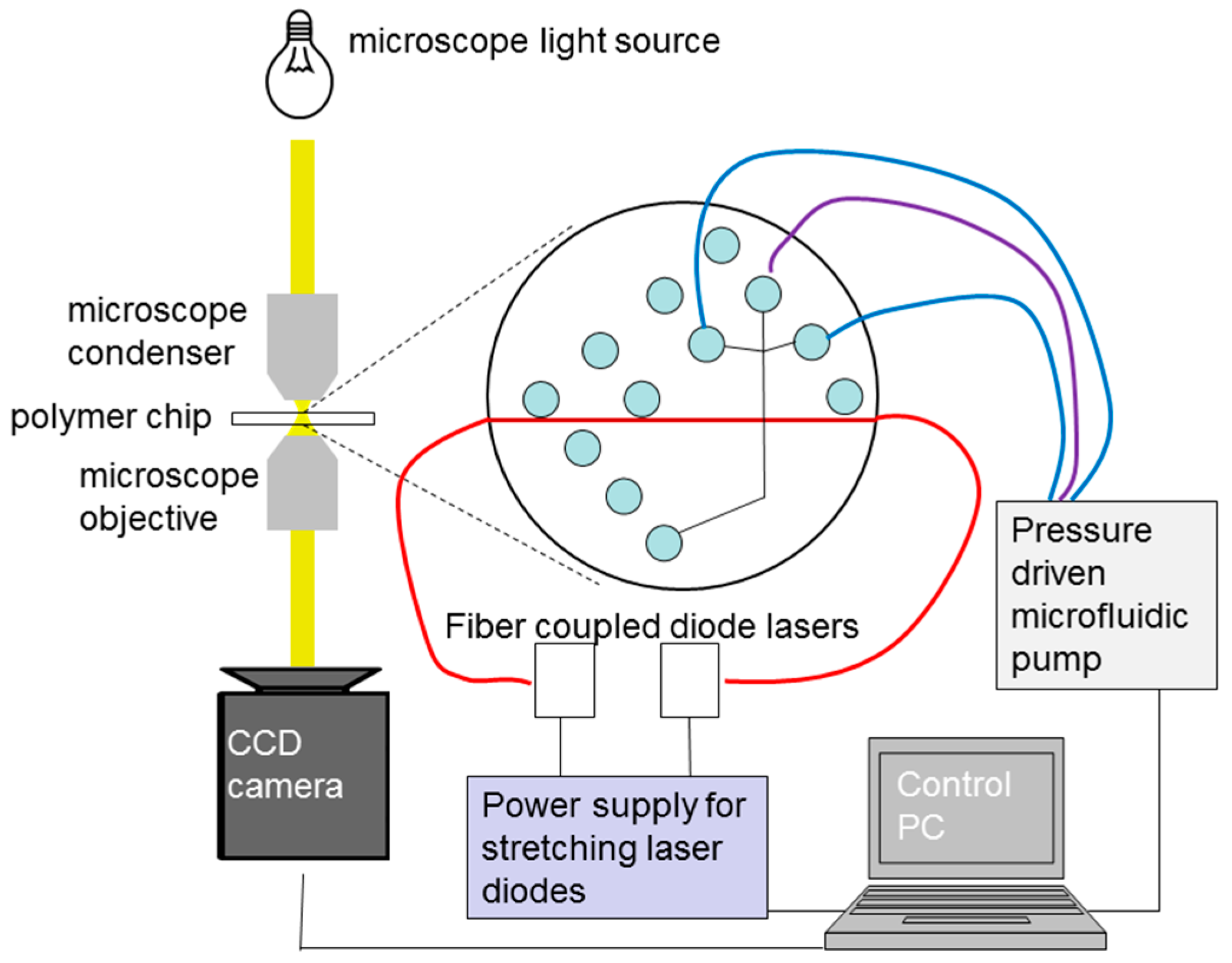
4.4. Raman Experiment Setup

The scheme of the setup for Raman experiments is shown in Figure 8. The optical system consisted of a green laser (Coherent Verdi, Santa Clara, CA, USA, 532 nm wavelength) which was coupled using an objective lens (Olympus RMS10X-PF, Tokyo, Japan, ×10 magnification, NA 0.3) and a 3-axis (XYZ) translation stage (Thorlabs MBT616D) to an input fiber (single-mode, SMF-28) which was inserted in the first chip. The maximum laser power launched into our system was 30 mW. An output fiber (multi-mode, Thorlabs FG050LGA) was inserted into a second chip and a HC fiber (NKT Photonics HC-1060-02, Birkerød, Denmark, 10 µm core diameter, 15 cm long) bridged the two chips. The HC fiber was chosen because of its favorable transmission properties after filling with water [31].
Figure 8. Diagram of optical and fluid system used in the Raman experiments.10× OL: 10× objective lens. XYZ: 3-axis stage for fiber alignment. SMF: single-mode fiber. MMF: multi-mode fiber. L2: lens. DM: dichroic mirror. NF: notch filter. PD: photodetector used to monitor the power. FC: fiber coupler. Dashed-arrows represent the flow direction.
Micromachines 06 01468 g008
At the output of the system, a dichroic mirror (Semrock Di02-R532-25×36, Rochester, NY, USA) and a notch filter (Thorlabs NF533-17) were used to separate the Raman scattered light from the pump laser light, which was coupled into a compact, fiber-coupled spectrometer (Thorlabs CCS200). The light reflected by the dichroic mirror was used to monitor the power output over time with a photodetector. The liquid filling system consisted of a peristaltic pump (Peristar Pro, WPI, Sarasota, FL, USA) and the chips were connected using standard connections (Male Luer lock with 1/16” barb fitting) and tubing (Tygon R3603, Saint Gobain Performance Plastics, Charny, France). Referring to Figure 1a), only the central inlet port was used for the filling. To allow air to escape from the chip during the initial filling, the other two inlet ports were open. During the experiment, these inlet ports were sealed with Luer caps.

5. Conclusions

A novel fabrication scheme for an optofluidic system with standard optical fibers that can be fabricated in large numbers has been reported. The system is intended to be fully fiber-based, removing the need for cumbersome alignment procedures and allowing external connection to fiber-coupled equipment (e.g., laser source, spectrometer, etc.). This produces a user-friendly optofluidic device that is quick and easy to assemble with highly reproducible optical characteristics.
Because of this high reliability, we have quickly obtained experimental setups for optical stretching, and by concatenating multiple chips, we created a system for in-fiber Raman spectroscopy. Therefore, we propose this technology as a practical solution for the training of students in LoC techniques.
We demonstrated a lateral fiber alignment to within 3 µm, where the main cause of misalignment is introduced by unwanted vertical movements in the fiber position during lid bonding. We suggest two improvements can be made in the design and manufacture of the chip: reducing the depth of the fiber groove to 125 μm and better control of lid swelling by optimizing the lid bonding recipe. Two further improvements in assembly can also be made: insertion of the fibers after lid bonding and the use of mechanical supports when inserting fibers.
Our fiber-based optofludic system allows high optical powers to be delivered to specimens without damaging the LoC system, thereby broadening the range of possible experiments (including stretching).
Further integration of advanced fiber-based components, e.g., fiber-based Bragg gratings [32], with the existing optical components, would allow the separation of signals of interest (e.g., Raman) and minimizing unwanted background signals (e.g., from silica). Further refinement of chip design (e.g., optimization of distance between the ends of the two cleaved fibers) will enhance the detection range and sensitivity for in-fiber Raman spectroscopy and other spectroscopic techniques. The technology and concepts reported here could be further developed into a compact system for in-line process measurements, for example measuring organic solvents in beverages [20] and protein concentration in media [6], where small volumes can be repeatedly assessed after appropriate flushing/cleaning methods. Fiber-based optofludics allow high optical powers to be delivered to specimens without damaging the LoC system, thereby broadening the range of possible experiments (including stretching).
Finally, the multilevel fabrication scheme described here can also be used to implement more complex geometries where optical and fluidic elements are separated [10,11], thus significantly broadening the number of possible LoC applications of the technology including optogenetic stimulation and detection [32], shape recognition [3], and flow cytometry [33].

Supplementary Materials

The following are available online at https://www.mdpi.com/2072-666X/6/12/1468/s1, Mask CAD design: OpTwe_01.cif, Video of cell stretching: Cellstr_rbc.wmv.

Acknowledgments

This work was supported by the Danish Council for Strategic Research through the Strategic Research Center PolyNano (grant no. 10-092322/DSF). The authors would like to acknowledge the PolyNano summer school, J. Emneus and the COST MP1205 initiative.

Author Contributions

The optofluidic chip was designed by Marco Matteucci, Kirstine Berg-Sørensen, Rafael J. Taboryski, and Anders Kristensen. Marco Matteucci designed the shim and produced the optofluidic chip. Marco Triches and Mark R. Pollard performed the Raman experiments. Giovanni Nava and Kirstine Berg-Sørensen performed the optical stretching experiments. All authors contributed to the writing of the manuscript.

Conflicts of Interest

The authors declare no conflict of interest. The founding sponsors had no role in the design of the study; in the collection, analyses, or interpretation of data; in the writing of the manuscript, and in the decision to publish the results.

References

  1. Psaltis, D.; Quake, S.R.; Yang, C. Developing optofluidic technology through the fusion of microfluidics and optics. Nature 2006, 442, 381–386. [Google Scholar] [CrossRef] [PubMed]
  2. Fan, X.; White, I.M. Optofluidic microsystems for chemical and biological analysis. Nat. Photonics 2011, 5, 591–597. [Google Scholar] [CrossRef] [PubMed]
  3. Schaap, A.; Bellouard, Y.; Rohrlack, T. Optofluidic lab-on-a-chip for rapid algae population screening. Biomed. Opt. Express 2011, 2, 658–664. [Google Scholar] [CrossRef] [PubMed]
  4. Khoury, M.; Vannahme, C.; Sørensen, K.T.; Kristensen, A.; Berg-Sørensen, K. Monolithic integration of DUV-induced waveguides into plastic microfluidic chip for optical manipulation. Microelectron. Eng. 2014, 121, 5–9. [Google Scholar] [CrossRef]
  5. Lai, C.W.; Hsiung, S.K.; Yeh, C.L.; Chiou, A.; Lee, G.B. A cell delivery and pre-positioning system utilizing microfluidic devices for dual-beam optical trap-and-stretch. Sens. Actuators B Chem. 2008, 135, 388–397. [Google Scholar] [CrossRef]
  6. Ferraro, J.; Nakamoto, K.; Brown, C.W. Introductory Raman Spectroscopy, 2nd ed.; Academic Press: New York, NY, USA, 2003. [Google Scholar]
  7. Nunes, P.S.; Ohlsson, P.D.; Ordeig, O.; Kutter, J.P. Cyclic olefin polymers: Emerging materials for lab-on-a-chip applications. Microfluid. Nanofluid. 2010, 9, 145–161. [Google Scholar] [CrossRef]
  8. Khetani, A.; Riordon, J.; Tiwari, V.; Momenpour, A.; Godin, M.; Anis, H. Hollow core photonic crystal fiber as a reusable Raman biosensor. Opt. Express 2013, 21, 12340–12350. [Google Scholar] [CrossRef] [PubMed]
  9. Østergaard, P.F.; Lopacinska-Jørgensen, J.; Pedersen, J.N.; Tommerup, N.; Kristensen, A.; Flyvbjerg, H.; Silahtaroglu, A.; Marie, R.; Taboryski, R. Optical mapping of single-molecule human DNA in disposable, mass-produced all-polymer devices. J. Micromech. Microeng. 2015, 25, 105002. [Google Scholar] [CrossRef]
  10. Kou, Q.; Yesilyurt, I.; Studer, V.; Belotti, M.; Cambril, E.; Chen, Y. On-chip optical components and microfluidic systems. Microelectron. Eng. 2004, 73–74, 876–880. [Google Scholar] [CrossRef]
  11. Kou, Q.; Yesilyurt, I.; Chen, Y. Collinear dual-color laser emission from a microfluidic dye laser. Appl. Phys. Lett. 2006, 88, 091101. [Google Scholar] [CrossRef]
  12. Constable, A.; Kim, J.; Mervis, J.; Zarinetchi, F.; Prentiss, M. Demonstration of a fiber-optical light-force trap. Opt. Lett. 1993, 18, 1867–1869. [Google Scholar] [CrossRef] [PubMed]
  13. Lincoln, B.; Schinkinger, S.; Travis, K.; Wottawah, F.; Ebert, S.; Sauer, F.; Guck, J. Reconfigurable microfluidic integration of a dual-beam laser trap with biomedical applications. Biomed. Microdevices 2007, 9, 703–710. [Google Scholar] [CrossRef] [PubMed]
  14. Suresh, S.; Spatz, J.; Mills, J.P.; Micoulet, A.; Dao, M.; Lim, C.T.; Beil, M.; Seufferlein, T. Connections between single-cell biomechanics and human disease states: Gastrointestinal cancer and malaria. Acta Biomater. 2005, 1, 15–30. [Google Scholar] [CrossRef] [PubMed]
  15. Ashkin, A.; Dziedzic, J.M.; Bjorkholm, J.E.; Chu, S. Observation of a single-beam gradient force optical trap for dielectric particles. Opt. Lett. 1986, 11, 288–290. [Google Scholar] [CrossRef] [PubMed]
  16. Guck, J.; Ananthakrishnan, R.; Mahmood, H.; Moon, T.J.; Cunningham, C.C.; Käs, J. The Optical Stretcher: A Novel Laser Tool to Micromanipulate Cells. Biophys. J. 2001, 81, 767–784. [Google Scholar] [CrossRef]
  17. PolyNano Summer School—Course Number 33692. Available online: http://www.kurser.dtu.dk/33692.aspx?menulanguage=en-gb) (accessed on 22 October 2015).
  18. Cubillas, A.M.; Unterkofler, S.; Euser, T.G.; Etzold, B.J.M.; Jones, A.C.; Sadler, P.J.; Wasserscheid, P.; Russell, P.S.J. Photonic crystal fibres for chemical sensing and photochemistry. Chem. Soc. Rev. 2013, 42, 8629–8648. [Google Scholar] [CrossRef] [PubMed]
  19. Maples, R.E. Petroleum Refinery Process Economics, 2nd ed.; Pennwell Pub: Nashua, NH, USA, 2000. [Google Scholar]
  20. Boyaci, I.H.; Genis, H.E.; Guven, B.; Tamer, U.; Alper, N. A novel method for quantification of ethanol and methanol in distilled alcoholic beverages using Raman spectroscopy. J. Raman Spectrosc. 2012, 43, 1171–1176. [Google Scholar] [CrossRef]
  21. Numata, Y.; Iida, Y.; Tanaka, H. Quantitative analysis of alcohol—Water binary solutions using Raman spectroscopy. J. Quant. Spectrosc. Radiat. Transf. 2011, 112, 1043–1049. [Google Scholar] [CrossRef]
  22. Tanzi, S.; Østergaard, P.F.; Matteucci, M.; Christiansen, T.L.; Cech, J.; Marie, R.; Taboryski, R.J. Fabrication of combined-scale nano-and microfluidic polymer systems using a multilevel dry etching, electroplating and molding process. J. Micromech. Microeng. 2012, 22, 115008. [Google Scholar] [CrossRef]
  23. Matteucci, M.; Christiansen, T.L.; Tanzi, S.; Østergaard, P.F.; Larsen, S.T.; Taboryski, R. Fabrication and characterization of injection molded multi level nano and microfluidic systems. Microelectron. Eng. 2013, 111, 294–298. [Google Scholar] [CrossRef]
  24. Jones, D.C.; Bennett, C.R.; Smith, M.A.; Scott, A.M. High-power beam transport through a hollow-core photonic bandgap fiber. Opt. Lett. 2014, 39, 3122–3125. [Google Scholar] [CrossRef] [PubMed]
  25. Ashok, P.C.; Singh, G.P.; Rendall, H.A.; Krauss, T.F.; Dholakia, K. Waveguide confined Raman spectroscopy for microfluidic interrogation. Lab Chip 2011, 11, 1262–1270. [Google Scholar] [CrossRef] [PubMed]
  26. Williams, G.O.S.; Chen, J.S.Y.; Euser, T.G.; Russell, P.S.J.; Jones, A.C. Photonic crystal fibre as an optofluidic reactor for the measurement of photochemical kinetics with sub-picomole sensitivity. Lab Chip 2012, 12, 3356–3361. [Google Scholar] [CrossRef] [PubMed]
  27. Utko, P.; Persson, F.; Kristensen, A.; Larsen, N.B. Injection molded nanofluidic chips: Fabrication method and functional tests using single-molecule DNA experiments. Lab Chip 2011, 11, 303–308. [Google Scholar] [CrossRef] [PubMed]
  28. Mucha, J.M.; Szytuła, A.; Kwiatkowska, C.J. Magnetic properties of nickel-vanadium alloys. J. Magn. Magn. Mater. 1984, 42, 53–58. [Google Scholar] [CrossRef]
  29. Seryogin, G.; Golovato, S.; Smith, S.; Williams, K.; Limburn, N.; Winn, A.; Mundada, G.; Adema, G. NiV Stress Control Utilizing PVD with an Ar/N2 Gas Mixture. In Proceedings of the 45th International Symposium on Microelectronics, San Diego, CA, USA, 9–13 September 2012; pp. 73–78.
  30. Buck, J.A. Fundamentals of Optical Fibers, 2nd ed.; John Wiley & Sons: Hoboken, NJ, USA, 2004. [Google Scholar]
  31. Antonopoulos, G.; Benabid, F.; Birks, T.A.; Bird, D.M.; Knight, J.C.; Russell, P.S.J. Experimental demonstration of the frequency shift of bandgaps in photonic crystal fibers due to refractive index scaling. Opt. Express 2006, 14, 3000–3006. [Google Scholar] [CrossRef] [PubMed]
  32. Bland-Hawthorn, J.; Ellis, S.C.; Leon-Saval, S.G.; Haynes, R.; Roth, M.M.; Löhmannsröben, H.G.; Horton, A.J.; Cuby, J.G.; Birks, T.A.; Lawrence, J.S.; et al. A complex multi-notch astronomical filter to suppress the bright infrared sky. Nat. Commun. 2011, 2, 581. [Google Scholar] [CrossRef] [PubMed] [Green Version]
  33. Guo, J.; Ma, X.; Menon, N.V.; Li, C.M.; Zhao, Y.; Kang, Y. Dual Fluorescence-Activated Study of Tumor Cell Apoptosis by an Optofluidic System. IEEE J. Sel. Top. Quant. Electron. 2015, 21, 7100107. [Google Scholar]

