3.1. Evaporation of Solvents
Since processes run in an open system, the evaporation rate of solvents (IPA and water) should be considered. The final volume of the etching solution was measured and compared to the initial volumes of dissolved KOH and IPA, to evaluate the evaporation rate of water and IPA.
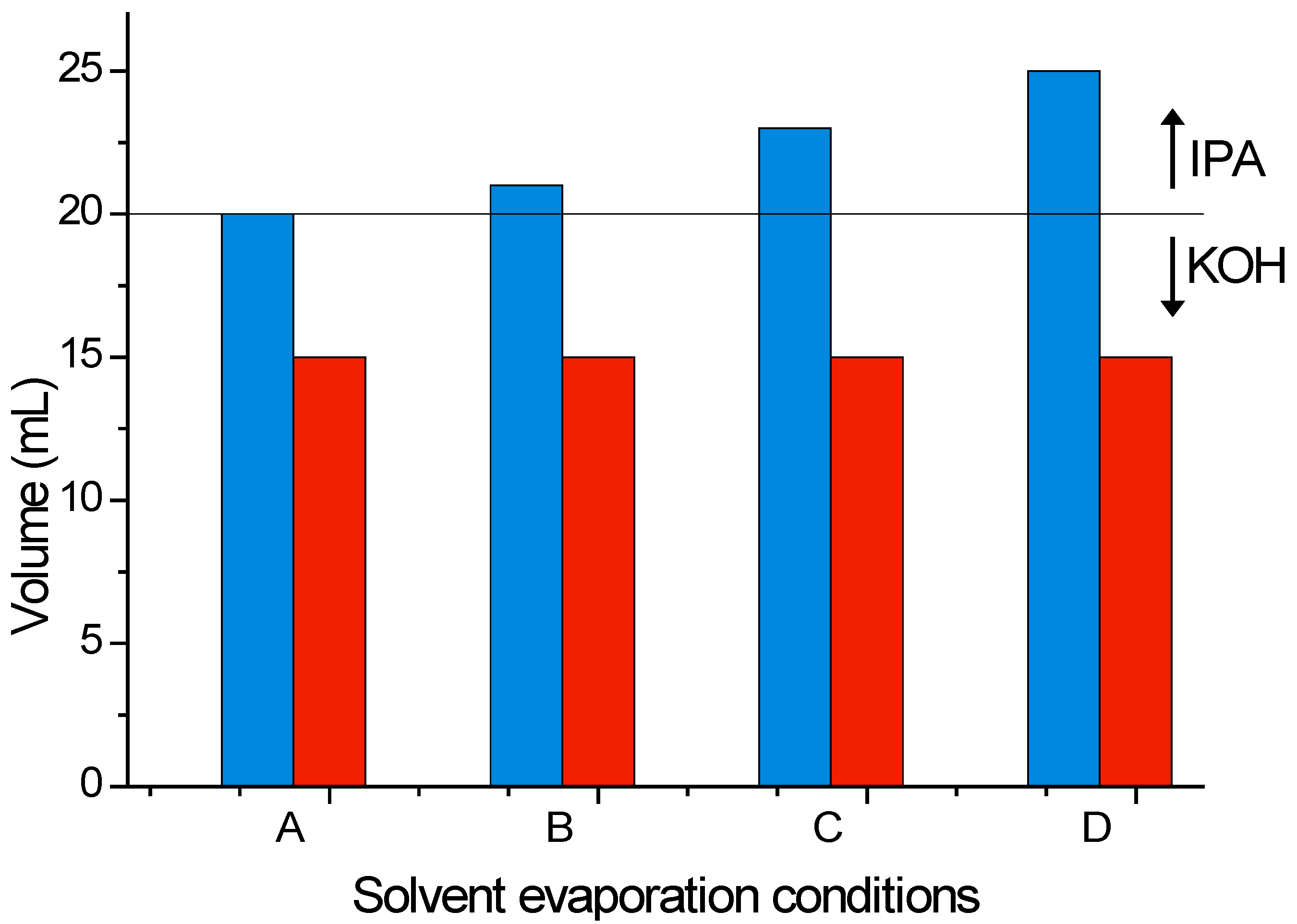
Each experiment started with an initial volume of 20 mL of 22 wt % KOH solution. A control sample, containing no added IPA, and three samples containing 1, 3 and 5 mL of initially added IPA, respectively, Sample B, C and D in
Figure 3, underwent a 120 min etching process under the same conditions.
Figure 3 summarizes the initial and final volumes of solution, upon process completion. Regardless of the amount of IPA initially added, given enough time (120 min here) all IPA evaporates and the final solution is only composed of dissolved KOH. The same final volume was achieved with the reference sample (Sample A, without addition of IPA), when applying the same process. From here it can be determined an approximate evaporation rate of 0.0417 mL/min for water vapor, and it can be concluded that the final volume is independent of the IPA content, if sufficient time is given to evaporate all IPA.
Four experiments were conducted to further study IPA influence, as described in
Table 1. For example, in Sample 4, from an initial volume of 40 mL (20 mL of KOH dissolved in water and 20 mL of IPA), 27 mL of etchant were available after 60 min. Approximately 2.5 mL of water were evaporated, considering the evaporation rate of 0.0417 mL/min described. Consequently, the remaining difference of 10.5 mL can be attributed to IPA evaporation, thus resulting in an evaporation rate of 0.175 mL/min. The errors in measuring the final volume (some droplets remained inside the HDPE flask) are estimated as a few hundred μL.
Table 1 shows the initial KOH and IPA content in solution for each Si wet etch process. The optimal etch time was inferred after periodic microscopic inspections, analyzing whenever the top mesa (
Figure 2) would detach from the remaining structure. This corresponds to a full patterned pyramid, with sharp vertices. This optimal etch time is dependent not only of the nominal size of each profile, but also of temperature, KOH concentration and IPA availability. In this work, IPA availability in the solution was tested, thus presenting different optimal etch times, with a time error estimated bellow 5 min, as a consequence of the initial volume of IPA added to the etching solution. At the optimal etch time, the final volume of solution was measured and the dissolved KOH and IPA volumes calculated. Considering initial volumes and evaporation rates, the IPA availability can be calculated (
Table 1), representing the amount of time necessary to evaporate all IPA in the etching solution.
Figure 3.
Graphical representation of the total initial volume (blue), as sum of initial KOH volume (20 mL) and IPA volume (0 to 5 mL), versus the final volume (red) after a total etching time of 120 min.
Figure 3.
Graphical representation of the total initial volume (blue), as sum of initial KOH volume (20 mL) and IPA volume (0 to 5 mL), versus the final volume (red) after a total etching time of 120 min.
Table 1.
Experimental conditions used in the definition of 10 μm × 10 μm wide pyramid structures through wet etching. IPA availability represents the predicted time at when all IPA would evaporate. If the “IPA availability” is greater than the “Etch time”, the etch process occurs entirely in the presence of IPA. Otherwise, a two phase process would occur (first with dissolved KOH and IPA, followed by dissolved KOH only).
| Sample | VKOH (mL) | VIPA (mL) | Etch Time (min) | Final Volume (mL) | IPA Availability (min) |
|---|
| 1 | 20 | 0 | 40 | 18 | 0 |
| 2 | 20 | 3 | 50 | 18 | 17 |
| 3 | 20 | 5 | 60 | 17 | 29 |
| 4 | 20 | 20 | 60 | 27 | 114 |
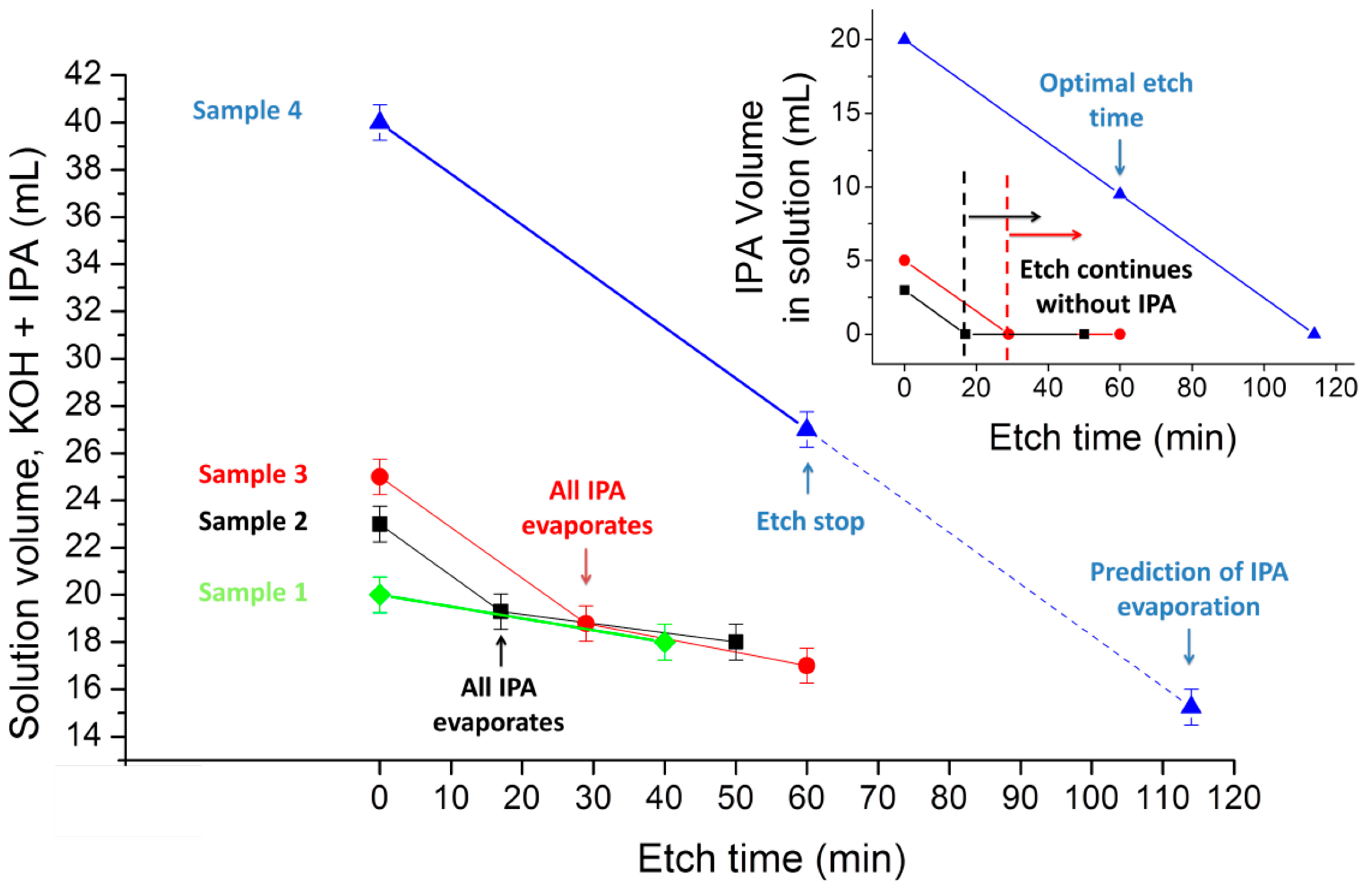
Sample 1 was used as a control sample, where IPA was never added. For Samples 2 and 3, the optimal etch time (50 and 60 min, respectively) was reached after the entire evaporation of IPA from the solution (achieved at 17 and 29 min, respectively). Sample 4 was etched in the presence of IPA during the entire process.
Therefore, IPA influence over the wet etching process of silicon can be measured in terms of availability, rather than concentration. Assuming that IPA is still in the solution, at any given time, and at a macroscopic level, variations in its concentration would not influence its effect.
Figure 4 further demonstrates the time evolution of this process.
Figure 4.
Evolution of solution volumes as a consequence of solvent evaporation. The main chart represents the volume of the whole solution (water and IPA) and the inset chart represents the IPA volume evolution, during the etch process. Sample 1 (green); Sample 2 (black); Sample 3 (red); and Sample 4 (blue).
The IPA availability effect is reinforced by results of a parallel etching process, containing an initial volume of 20 mL dissolved KOH and 2 mL IPA, and then adding 2 mL IPA every 10 min, ensuring that IPA is always available during the entire etching process (evaporation rate of 0.175 mL/min was observed, as previously described). The macroscopic etching results from this experiment are quite similar from those obtained in Sample 4, and distinguishable from every other sample. The same etching profile can be achieved either with an initial saturated solution, or with a lower, but continuously assured, concentration of IPA.
We can support that, after the expected evaporation time has been achieved, the wet etching process will continue in the same conditions as Sample 1 (without IPA). Therefore, we have two specific moments that are particularly relevant to the etching process: when IPA is still present in the solution and when all IPA evaporates.
3.2. Influence of IPA in the Wet Etch of Silicon
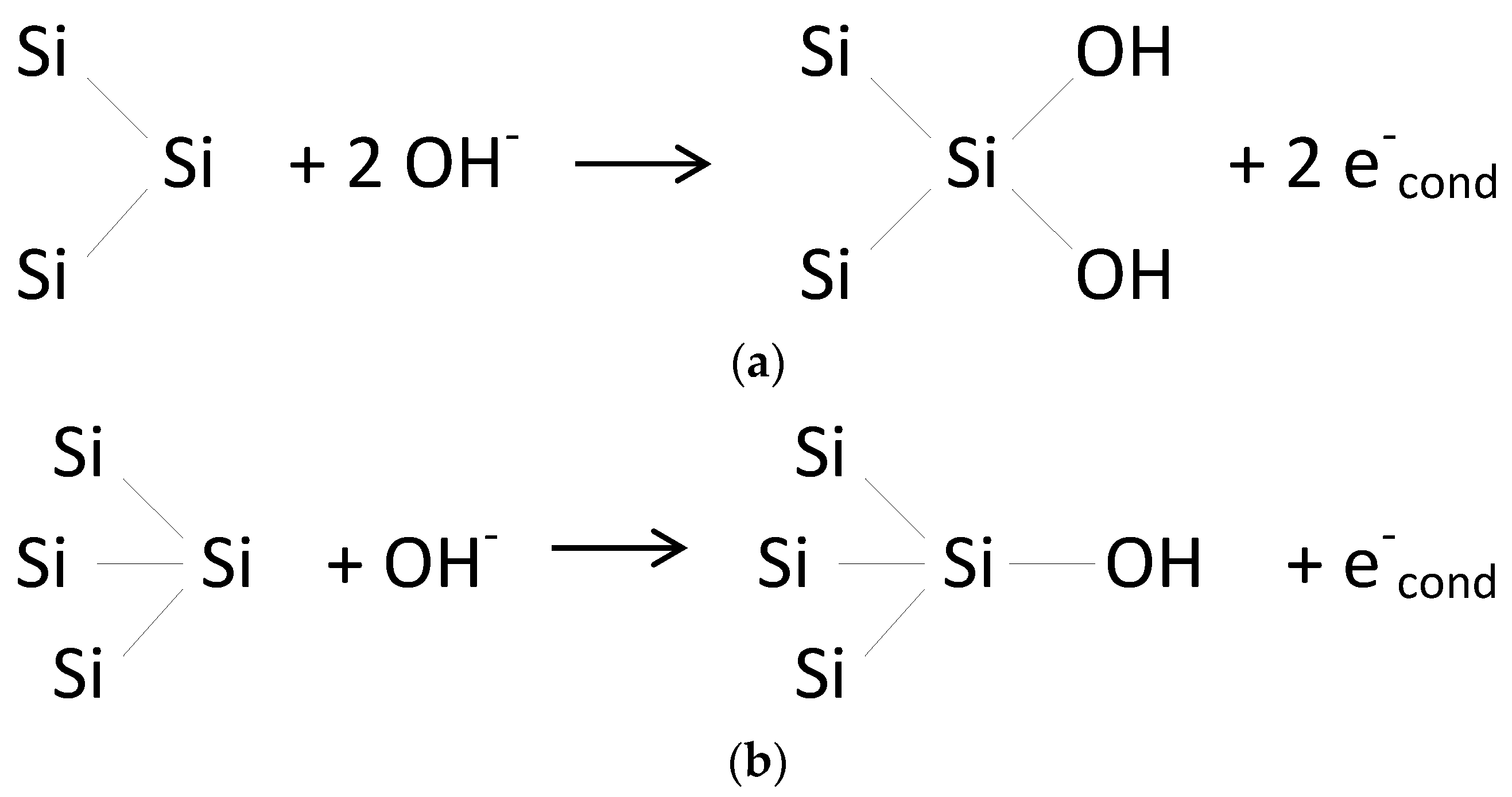
The etch rate for the (110) and (331) planes can be 2× and 1.5× larger than the etch rate for the (100) plane, respectively, in KOH etching solutions [
12]. This results in a very sharp, but irregular structure with a very marked underetching profile. The obtained structures present an octagon base with a basal diameter up to 1/3 and height up to 1/4 of the profile nominal size (mask size), thus illustrating a severe underetch. However, the etching rate of specific planes in silicon KOH etching can be modulated through IPA. The addition of IPA to the etching solution greatly reduces the etch rate in these planes down to 8× lower [
12]. In these conditions, the (110) plane is predominantly protected, thus significantly increasing the base diameter of the structure and reorienting it towards the (100) axis. As the etching undergoes in saturated conditions (where IPA is thoroughly present in the process), the structures maintain a square shape aligned with the axis, whilst increasing base width (
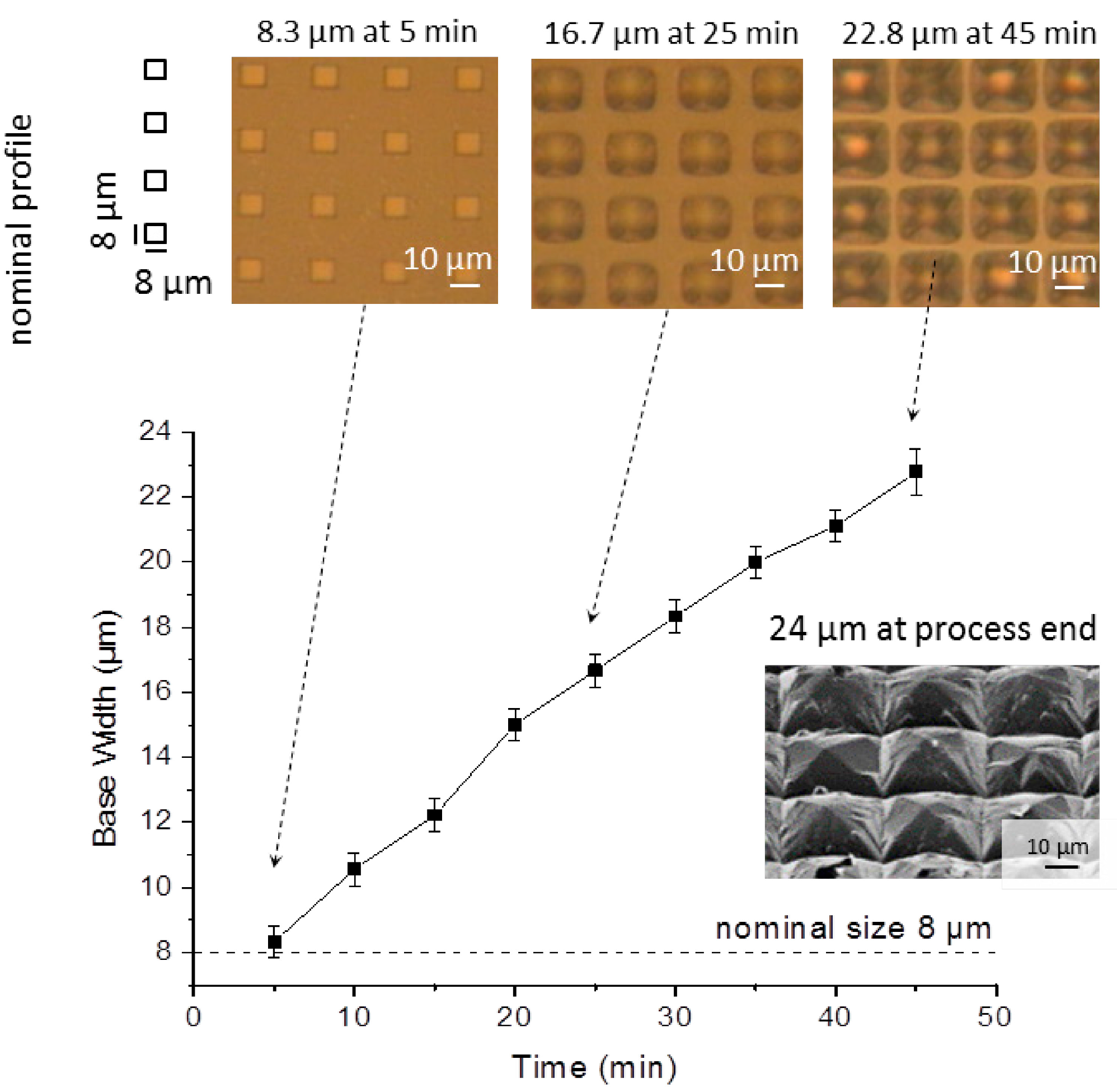
Figure 5). Due to this progressive increase and profile spacing, the structures end up colliding upon their edges. Therefore, spacing between adjacent profiles needs to be carefully planned to prevent grouping.
Figure 5.
Evolution of base width, along the wet etch process, obtained from a 8 μm × 8 μm square mask with a spacing of 16 μm, under IPA saturated conditions, as described for sample 4 in
Table 1. Top view microscope images show how the individual square patterns are enlarged and merged together.
Figure 5.
Evolution of base width, along the wet etch process, obtained from a 8 μm × 8 μm square mask with a spacing of 16 μm, under IPA saturated conditions, as described for sample 4 in
Table 1. Top view microscope images show how the individual square patterns are enlarged and merged together.
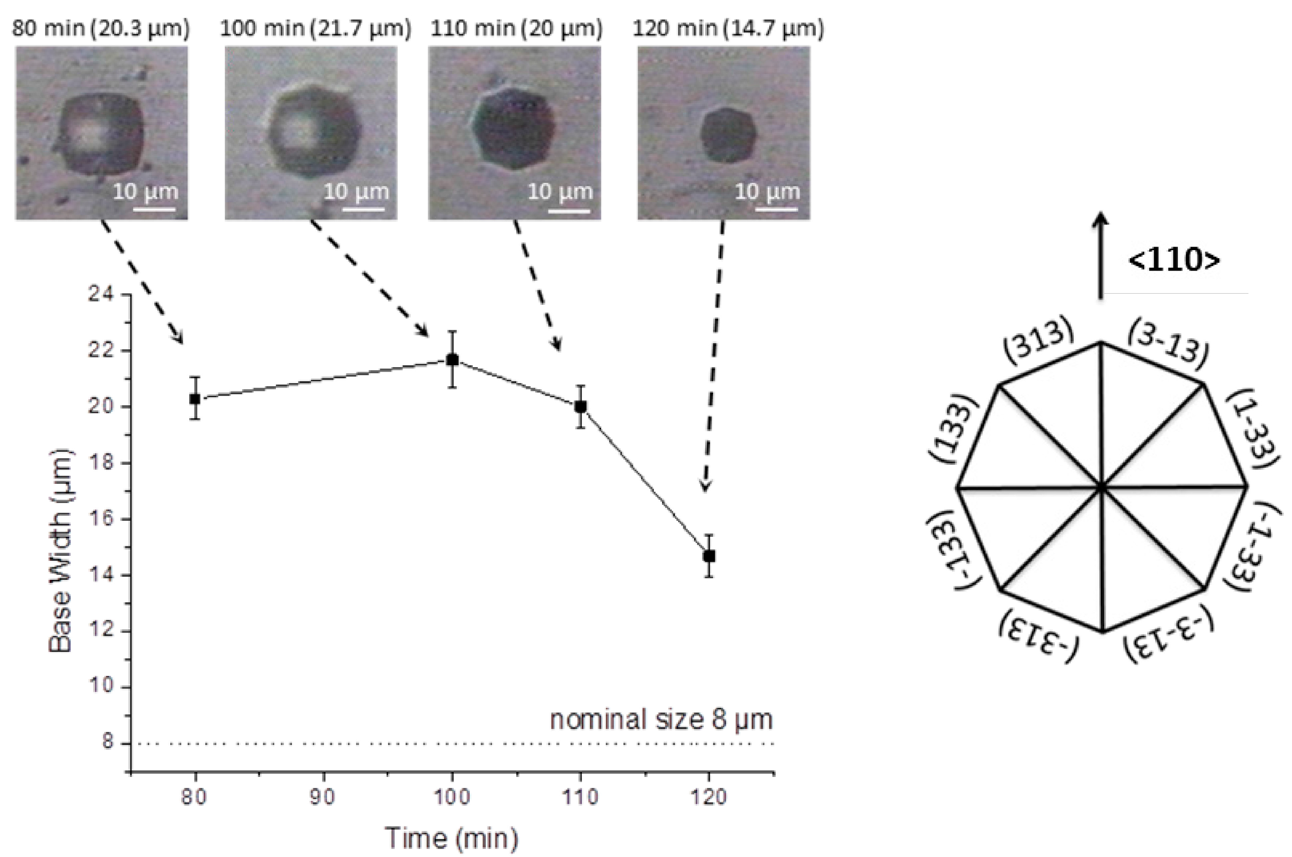
The structure base width starts to recede after complete evaporation of IPA, as a more pronounced (110) etch is performed in the absence of IPA. Moreover, the increase etch rate of the (331) plane promotes the transition from a square shaped to an octagonal shaped structure, as seen in
Figure 6. At this stage, this transition occurs progressively, and is independent of the overlaying mask, since the structure width has grown beyond the nominal size, and therefore, is no longer defined by it. As observed in the images representative for the etching process after 80 and 100 min, within
Figure 6, the reorientation of the structure shape occurs whilst the initial mask, shown as a bright square, remains overlaid to the dark structure.
Figure 6.
Top view microscopic images demonstrating the evolution of base width, upon the wet etch process, obtained from a 8 μm × 8 μm square mask with a spacing of 40 μm, after IPA evaporation. This process occurred first as described in
Figure 5 (up to 80 min), but with an increased spacing as to prevent merging, followed by etching in solution without IPA (after 80 min).
Therefore, modulating the availability of IPA at any given time during the wet etch process allows for a more precise control of the final structure. The initial IPA volume necessary to keep IPA availability until the etch process depends not only on exposed silicon area and the desired etch depth, but also on the volume and surface area of the etching solution.
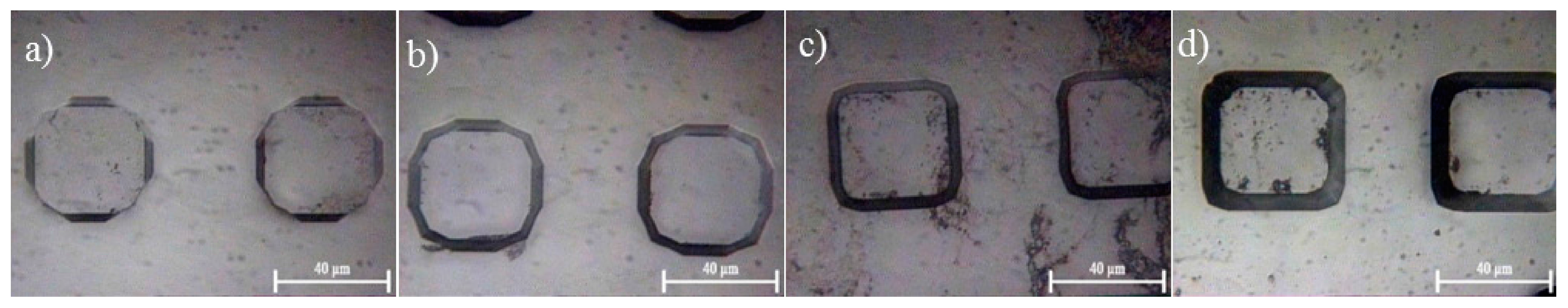
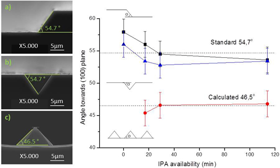
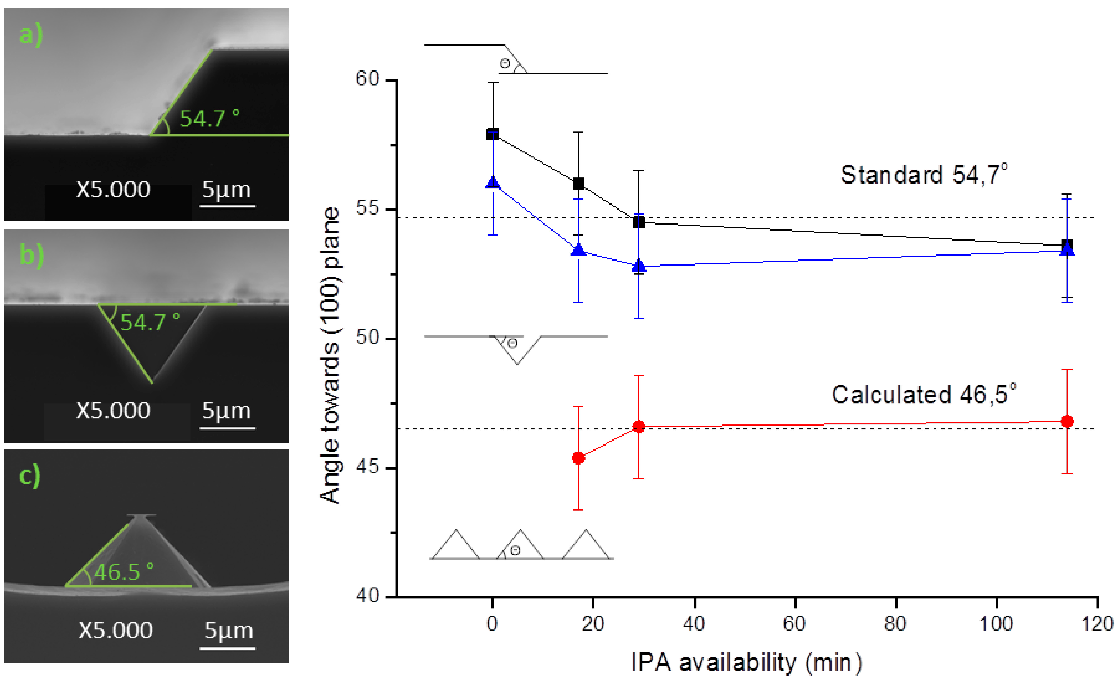
Each sample was patterned with three mask profiles as depicted in
Figure 7: (a) 200 μm wide rectangular mask; (b) 10 μm square mask with a spacing of 20 μm, for v-grove patterning; and (c) 10 μm square mask with a spacing of 20 μm. SEM imaging was used in the determination of pyramid lateral angles. All samples reveal a consistency towards each angles, and by consequence, towards each planes. Three profiles were obtained at same time instants (for each sample, in the same etch solution), and by consequence, with the same IPA availability.
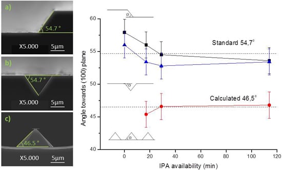
Figure 7.
Evolution of measured patterns angle in different IPA availability conditions, obtained from: (a) 200 μm wide rectangular mask (black); (b) 10 μm v-grove from a square mask with a spacing of 20 μm (blue); and (c) 10 μm square mask with a spacing of 20 μm (red).
Figure 7.
Evolution of measured patterns angle in different IPA availability conditions, obtained from: (a) 200 μm wide rectangular mask (black); (b) 10 μm v-grove from a square mask with a spacing of 20 μm (blue); and (c) 10 μm square mask with a spacing of 20 μm (red).
As seen in
Figure 7a,b, the 200 μm wide pattern and the v-groves present a 54.7° ± 2° angle, characteristic of the (111) plane. This result was obtained independently of the IPA volume added to the etch solution, and is in accordance with the expected results. When defining grooves, the etched structure always orientates to align with the wafer flat, forming squared pyramids with (111) planes. IPA influence on the final profile is negligible, either on the base width or profile topography. Typically, the end result is a uniform etch, as in
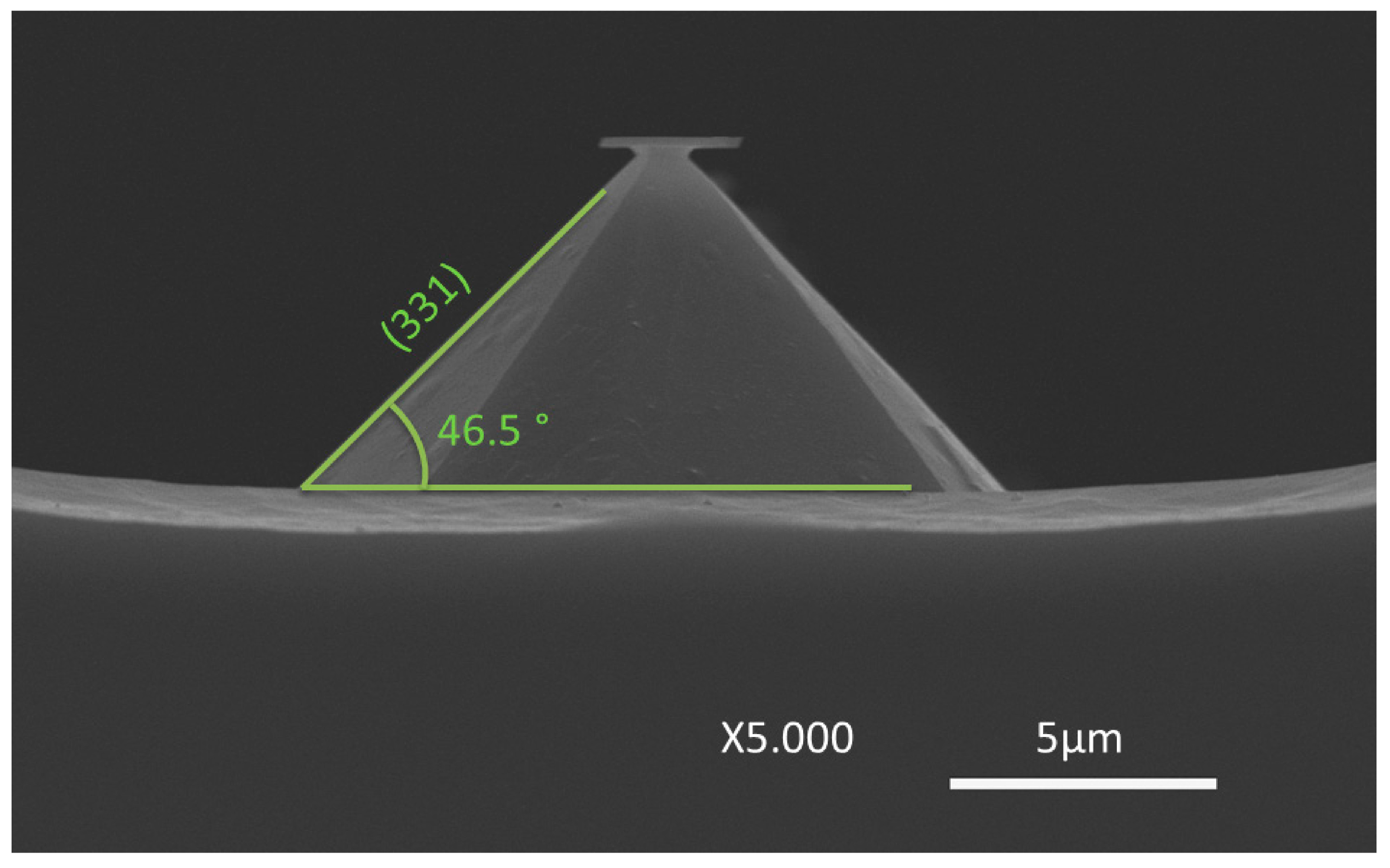
Figure 7b. However, dense structures are deeply influenced by the neighboring topography, which can be seen, in
Figure 7c, by the angle decrease to 46.5°. IPA concentration plays little influence in the final patterning result, but its absence originates a structure with a rough etch hardly quantifiable by SEM analysis.
The discrepancy between the results from
Figure 7a,c is focused only on the adjacent area around each of the structures. While the first portrays a long line that was patterned 200 μm apart from any other structure, the latter depicts structures patterned in a dense array. The difference can be attributed to microloading effect, in which etchants and byproducts of the reaction have more difficulty diffusing through smaller areas [
17]. Therefore, in dense arrays of structures, as soon as the wet etch begins, the (100) plane is less accessible than the (110) plane. In order to modulate this scenario, the desired structures may be patterned further apart, or additives can be incorporated in the etching solution in order to increase the wettability of the silicon wafer. On the contrary, v-groves are not affected by the microloading effect, and denser arrays of pyramidal structures with sharper edges can be patterned. All the v-grove structures are formed with a square base, independently of the nominal profile shape (mask) or orientation.
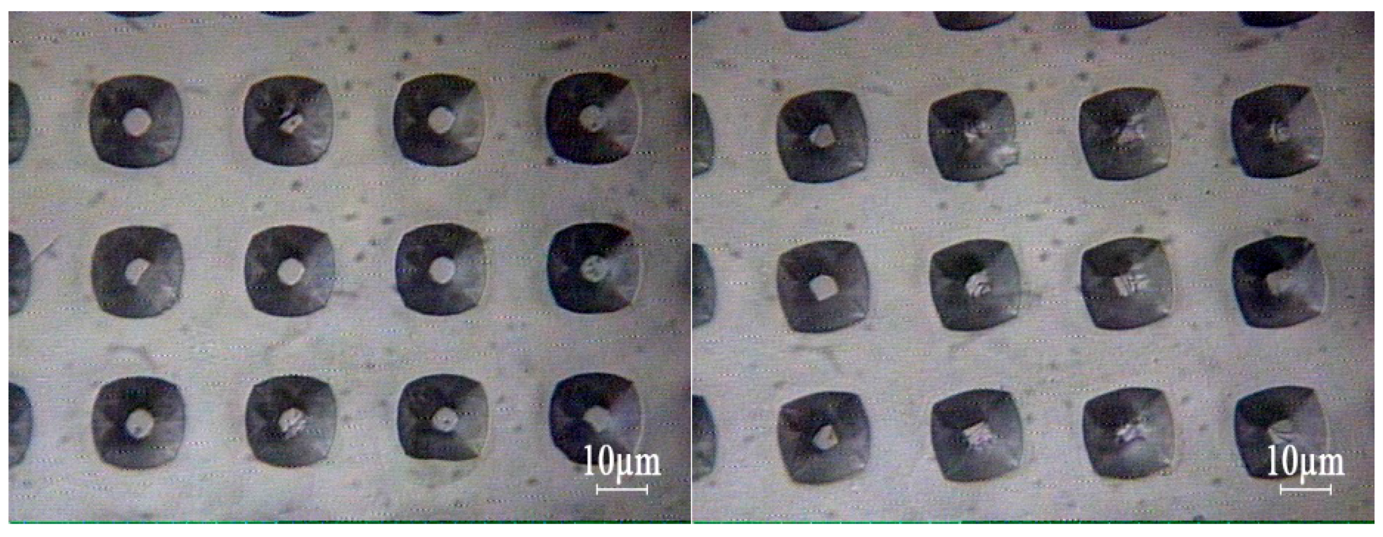
Figure 8 demonstrates in detail the result of the microloading effect depicted in
Figure 7c.
Figure 8.
SEM cross-section image of the structure obtained with a 10 μm × 10 μm square mask, spaced 20 μm from the next square, in a 22 wt % KOH wet etch process (Sample 2 in
Table 1).
Figure 8.
SEM cross-section image of the structure obtained with a 10 μm × 10 μm square mask, spaced 20 μm from the next square, in a 22 wt % KOH wet etch process (Sample 2 in
Table 1).
IPA availability takes an important role defining the etched structure in top view SEM images. Near the optimal volume of IPA, the influence on the number of etched planes is maximized. Squares aligned with the wafer flat will have reorientation, initially to a dodecahedron, and finally to an octagon profile, as seen in
Figure 9a. This will result in an octagonal pyramid with faces oriented towards the (331) plane.
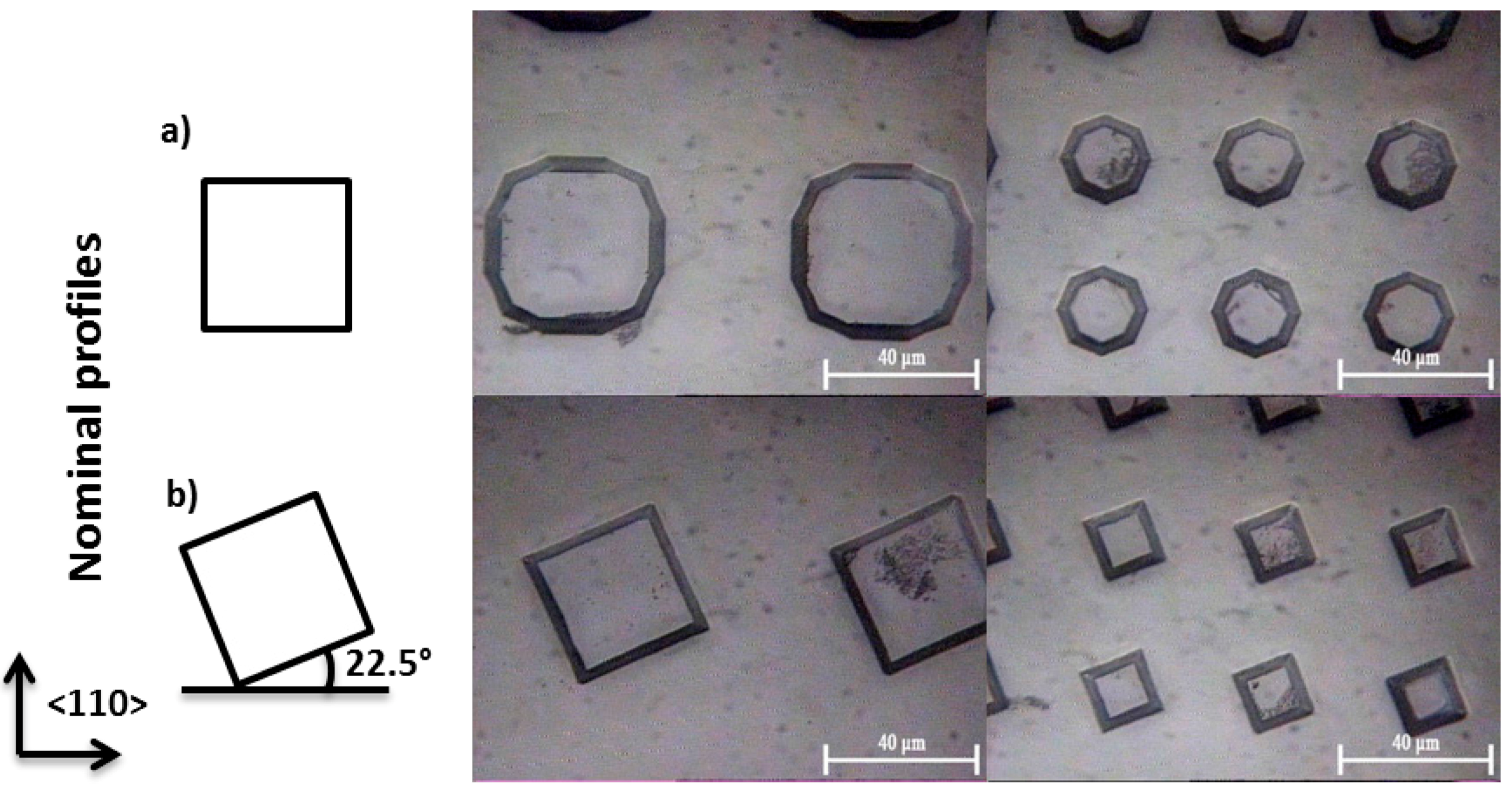
Figure 9.
Microscopic inspection of a 22 wt % KOH wet etch process, (Sample 2, in
Table 1) after 20 min. Initial profile: (
left) 40 μm and (
right) 20 μm; square: (
a) aligned with the wafer flat; and (
b) misaligned 22.5° with the wafer flat.
Figure 9.
Microscopic inspection of a 22 wt % KOH wet etch process, (Sample 2, in
Table 1) after 20 min. Initial profile: (
left) 40 μm and (
right) 20 μm; square: (
a) aligned with the wafer flat; and (
b) misaligned 22.5° with the wafer flat.
When exposing a squared profile, tilted 22.5°, to the same etching conditions, the result are squared pyramids with no reorientation, as shown in
Figure 9b. In fact, this is the same etching plane that is replicated bi-dimensionally in structures aligned with the wafer flat, such as those in
Figure 9a. A predominance to etch in these planes, forming the structural pyramids described in
Figure 6, protects those in
Figure 9b from any reorientation. An equal result can be obtained when rotating the same misaligned profile by 45°. This way, it is possible to exactly define the desired structure, between a squared and octagonal shape profile, only by modifying the alignment towards the wafer flat.
Alternatively, higher volumes of IPA will form structures with rounder shapes, independently of profile orientation, as demonstrated in
Figure 10. The surface topography, however, is much rougher in these conditions and structural uniformity is hard to achieve.
Figure 10.
Microscopic inspection of a 22 wt % KOH, saturated with IPA, wet etch process, (Sample 4 in
Table 1) after 50 min. Initial profile: 10 μm squares (
left) aligned and (
right) misaligned 22.5° with the wafer flat.
Figure 10.
Microscopic inspection of a 22 wt % KOH, saturated with IPA, wet etch process, (Sample 4 in
Table 1) after 50 min. Initial profile: 10 μm squares (
left) aligned and (
right) misaligned 22.5° with the wafer flat.
An evolution of this process can be observed in
Figure 11. As demonstrated previously, in the absence of IPA, the KOH etches the (110) plane predominantly, which causes the visible undercut etch seen in
Figure 11a. A 17 min availability of IPA in the beginning of the process is sufficient to stabilize the etching rates for the (110) and (331) planes, thus allowing the formation of octagonal structure (
Figure 11b). However, with the increase of IPA availability, the square profile is maintained with rounder edges, as observed in
Figure 11c,d.
Figure 11.
Microscopic inspection of a 22 wt % KOH wet etch process after 20 min. Initial profile: 40 μm squares aligned with the wafer flat. Conditions are described in
Table 1: (
a) Sample 1; (
b) Sample 2; (
c) Sample 3; and (
d) Sample 4.
Figure 11.
Microscopic inspection of a 22 wt % KOH wet etch process after 20 min. Initial profile: 40 μm squares aligned with the wafer flat. Conditions are described in
Table 1: (
a) Sample 1; (
b) Sample 2; (
c) Sample 3; and (
d) Sample 4.
Once IPA evaporates, these profiles tend to revert to a situation as in
Figure 11a, given the width of the structure is enough to allow for a gradual profile reorientation, before the etching reaches the
mesa release stage. For the experimental conditions tested, a threshold is held for the IPA availability between 17 and 29 min. However, since the structures observed in
Figure 11 are wide enough for the etching to proceed, a longer etching could, eventually, allow for the correction of the etched planes as a consequence of KOH increasing (110) and (331) etch rate.
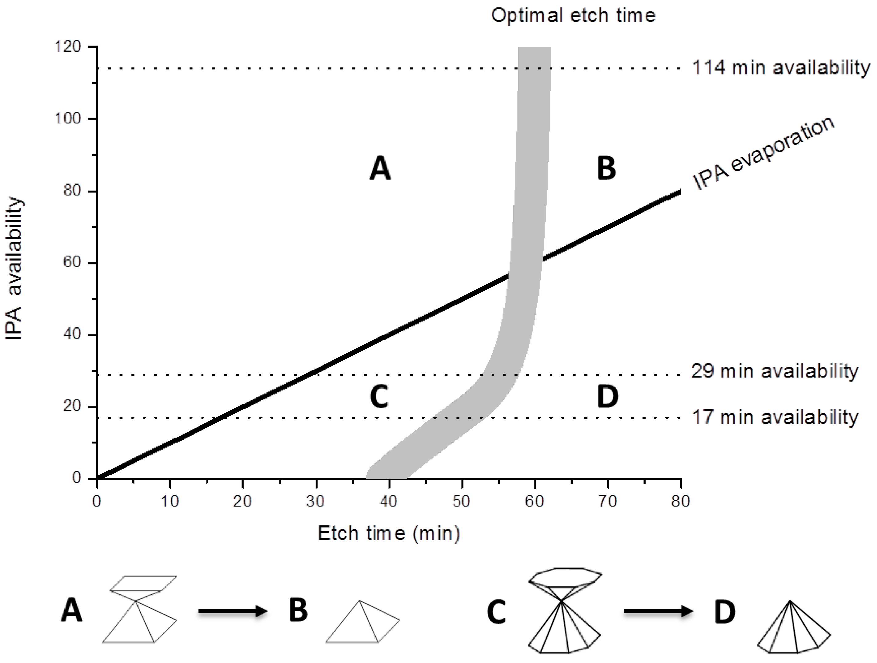
As a summary,
Figure 12 presents a diagram relating the etching profiles obtained along the etching evolution time, with the IPA availability. In general, square patterns are transferred to silicon under a squared-based pyramid (transition from region A to B) whenever a minimum level of IPA is maintained in solution. On the contrary, square based pyramids (region A) may rearrange along etching time into n-side polygons (region C) if meanwhile there is no IPA available in the solution. This transition is gradual and, at any given time, the structure shape is dependent on profile size and etch rate. Continuing the etching until the top mesa is released (optimal etch time) can stabilize the octagonal base pyramidal shape (region D).
Figure 12.
Schematic diagram of the evolution of silicon wet etch structures, under IPA influence, for a 10 μm square mask and the conditions depicted in
Table 1.
Figure 12.
Schematic diagram of the evolution of silicon wet etch structures, under IPA influence, for a 10 μm square mask and the conditions depicted in
Table 1.


 ,
, 


