Article

Optimisation Design of Coupling Region Based on SOI Micro-Ring Resonator

1
Key Laboratory of Instrumentation Science and Dynamic Measurement of Ministry of Education, North University of China, Taiyuan 030051, Shanxi, China
2
Science and Technology on Electronic Test & Measurement Laboratory, North University of China, Taiyuan 030051, Shanxi, China
*
Author to whom correspondence should be addressed.
These authors contributed equally to this work.
Micromachines 2015, 6(1), 151-159; https://doi.org/10.3390/mi6010151
Submission received: 14 November 2014 / Accepted: 25 December 2014 / Published: 31 December 2014

Abstract

:
Design optimization of the coupling region is conducted in order to solve the difficulty of achieving a higher quality factor (Q) for large size resonators based on silicon-on-insulator (SOI). Relations among coupling length, coupling ratio and quality factor of the optical cavities are theoretically analyzed. Resonators (R = 100 μm) with different coupling styles, concentric, straight, and butterfly, are prepared by the micro-electro-mechanical-systems (MEMS) process. Coupling experimental results show that micro-cavity of butterfly-coupled style obtains the narrowest (3 dB) bandwidth, and the quality factor has been greatly improved. The results provide the foundation for realization of a large size, high-Q resonator, and its development and application in the integrated optical gyroscopes, filters, sensors, and other related fields.

1. Introduction

For the development of navigation technology, the requirements of integrated optical gyros [1,2,3] will continue to increase, and some development routs now proposed take into account miniaturization, low cost, low power consumption, mass production, and gyro accuracy. As the core component of an integrated optical gyroscope, an optical micro-cavity realizes the measurement of the rotational angular velocity through the principle of resonance and Sagnac effect. Waveguide resonators based on silicon-on-insulator (SOI) have been of interest in optical gyros, particularly optical waveguide gyros, due to the advantages in their simple structure, high integration and high sensitivity. Optical cavities with large-size and higher quality factor (Q) value become the key components in optical waveguide gyroscopes for the detection limit to be further improved. However, due to the current level of technology, the larger size of optical cavities leads to greater transmission loss, which is not conducive to improvement of the quality factor.
Some scholars start researching from a surface-smoothing process to reduce the transmission loss [4,5] in order to achieve high-Q values, but the amount of research completed is low and has not had a significant effect. Here, we pay attention to the optimal design in the coupling region of the large-size ring resonator, and theoretically analyze the relationships between the coupling length, coupling coefficient and quality factor. Through the coupling experiments of three kinds of coupling in SOI ring resonators (R = 100 μm), we obtain a new type of butterfly-coupled structure. Thus, the larger sized optical cavity (R = 642 μm) and higher-Q value (up to five times the power) is produced without any surface treatment. This study is helpful for the achievement of optical cavities with a large size and high-Q value, which not only provides an important basis for the research of integrated optical gyroscopes, but is also propitious to their applications in the filters [6,7,8], modulators [9], biological sensing detection [10,11] and other related fields.

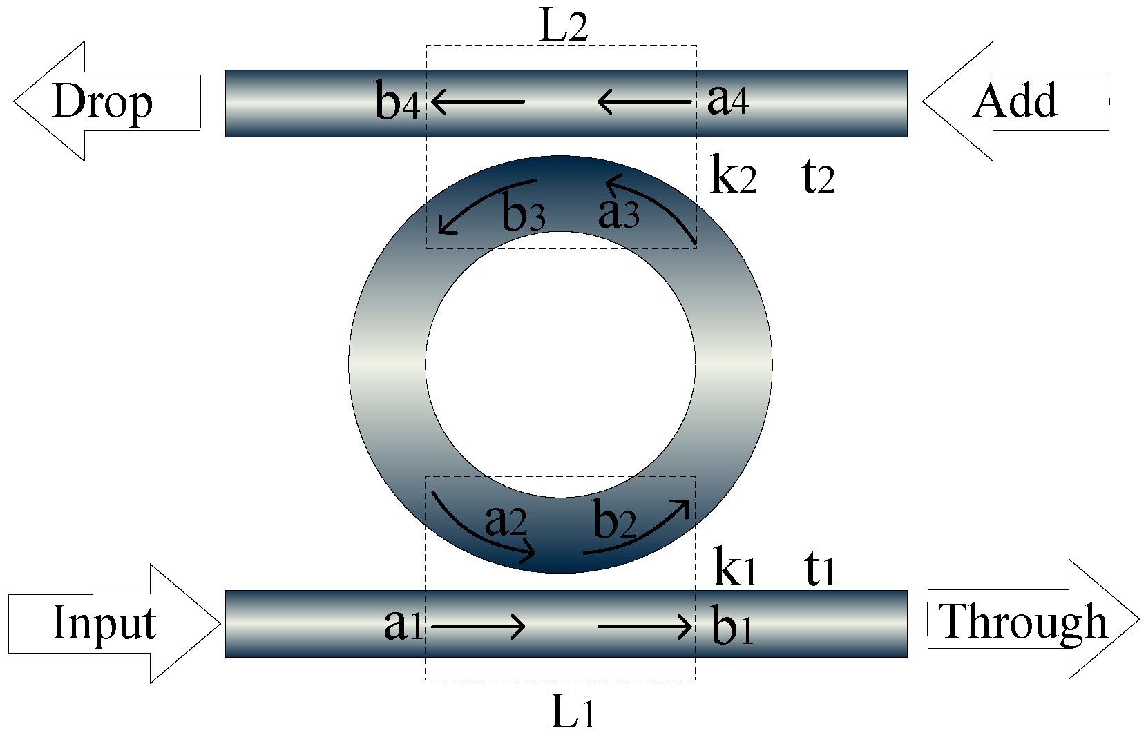
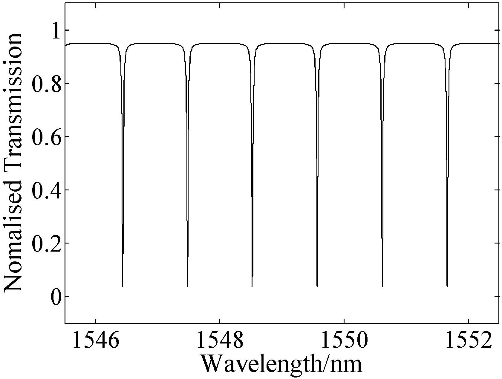
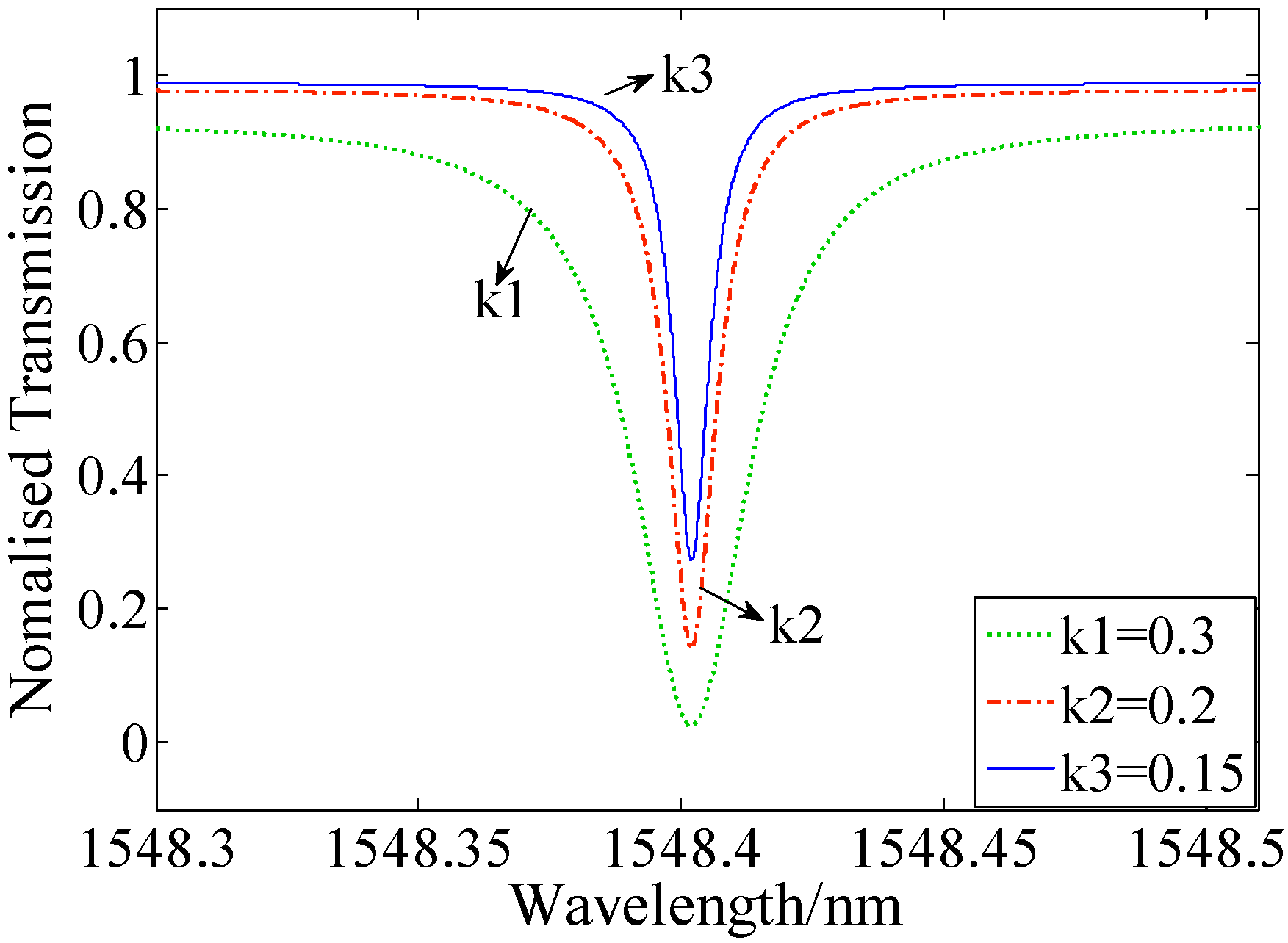
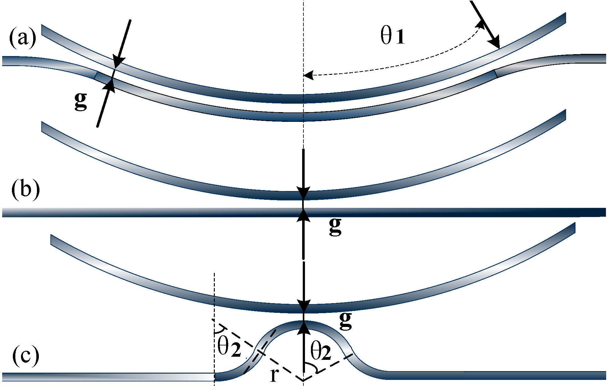
2. Transmission Characteristics in Micro-Cavity

A typical optical field transmission of ring resonator is shown in Figure 1, where k(k1,k2) and t(t1,t2) are amplitude coupling ratios, and transmission ratios in coupling regions as shown in virtual boxes, a(a1,a2,a3,a4) and b(b1,b2,b3,b4), respectively, represent the input and output optical field. In the case of ignoring back-scattering (a4 = 0), the transfer function of the optical field in the through port can be obtained by the transfer matrix method [12] as shown in Equation (1):
H = | b 1 a 1 | 2 =   | [ t 1 t 2 exp ( j 2 Φ α r i n g ) ] exp ( j 2 Ψ α L ) 1 t 1 t 2 exp ( j 2 Φ α r i n g ) | 2
where, Φ and Ψ are phase shifts separately caused by transmission of half circle (πR) and channel waveguide of coupling distance (L), expressed as:
Φ = 2 π N e f f l / λ   =   2 π 2 N e f f R / λ ,   Ψ =   2 π N e f f L / λ
aring = R, aL = a·L, respectively, indicate transmission loss in circumference (2πR) of ring resonator and coupling distance (L) of channel waveguide, a is the loss coefficient, λ and Neff represent transmission wavelength and the effective refractive index of the micro-ring resonator. Assuming t1 = t2 = t, k1 = k2 = k and t2 + k2 = 1, the transfer function in Equation (1) will be given by:
H =   | ( 1 k 2 ) 1 2 [ 1 exp ( j 2 Φ α r i n g ) ] exp ( j 2 Ψ α L ) 1 ( 1 k 2 ) exp ( j 2 Φ α r i n g ) | 2
supposing the radius of resonator is 100 μm, simulation of transmission characteristics and resonance spectrums in different coupling ratios (k) are, respectively, shown in Figure 2 and Figure 3.
Figure 1. Schematic diagram of optical field transmission of a two-path ring resonator.
Micromachines 06 00151 g001
Figure 2. Resonance spectrum of ring resonator (R = 100 μm).
Micromachines 06 00151 g002
Figure 3. Resonance spectrums with different coupling ratios (R = 20 μm).
Micromachines 06 00151 g003
It can be seen from Figure 3, smaller coupling coefficient achieves weaker coupling strength, and the depth of resonance will decrease at the same time. With that, the full width at half the resonance spectrum maximum (3 dB bandwidth) becomes narrower, thus obtaining a high-Q value. The simulation above shows that changing the coupling form, such as controlling effective coupling length and gaps in a reasonable range of resonance depth, cavities with diverse coupling ratios can be achieved to meet different needs for research and application. In the case of a fixed coupling gap, the coupling ratio (k) changes as the absolute value of a sine form related to the coupling length Lc in general, while the ratio k becomes larger with the increasing Lc in a certain range [13,14,15], therefore, we decided to get different k through design optimization by controlling the coupling length to improve the quality factor.

3. Process and Experiment

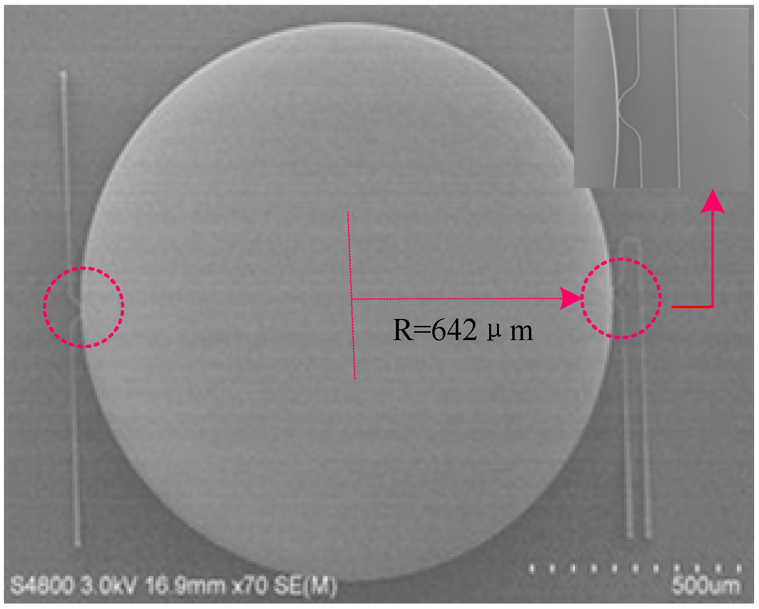
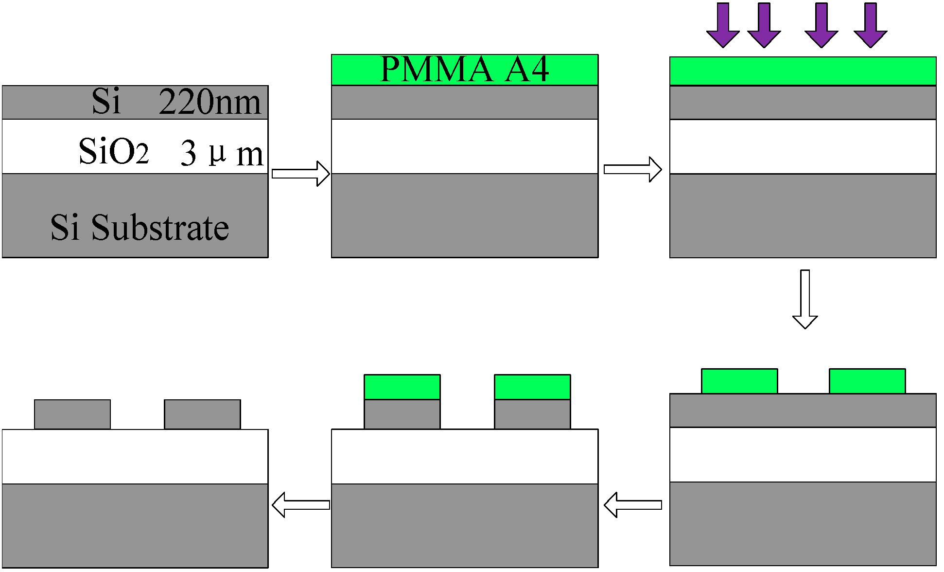
3.1. Preparation of Optical Cavity
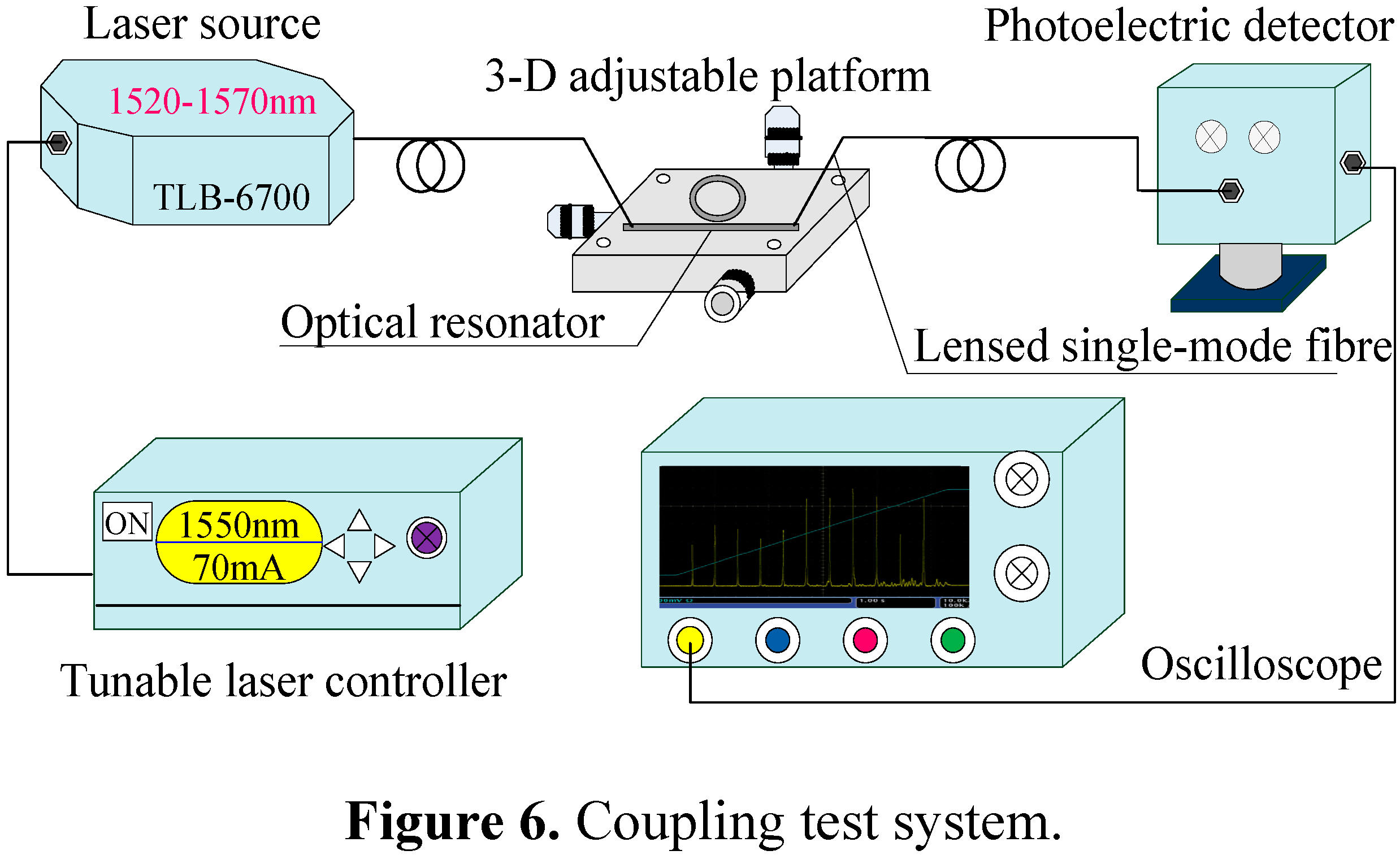
SOI is the common material used in optical resonators due to its excellent ability to restrict the optical field for the large refractive index difference between the waveguide layer (Si) and confinement layer (SiO2). SOI ring resonators with the same radius (100 μm) and different coupling forms are fabricated by micro-electro-mechanical-systems (MEMS) process. The cavities are mainly composed of the top silicon with 220 nm height and ~500 nm width. Several process and coupling design diagrams are shown in Figure 4 and Figure 5. Here, the coupling angle (2θ1) is 60° in concentric-coupled (a), θ2 (60°) and coupled-waveguide arc-radius (r = 15 μm) are designed in butterfly-coupled (c), and all the coupling gaps (g) are ~110 nm.
Figure 4. Fabrication process of optical micro-cavity.
Micromachines 06 00151 g004
Figure 5. Schematic of coupling regions: (a) Concentric-coupled. (b) Straight-coupled. (c) Butterfly-coupled.
Micromachines 06 00151 g005
As is demonstrated in Figure 4, the device is spin-coated by an electron beam resist polymethyl methacrylate A4 (PMMA A4), and exposed in the electron-beam-lithography (EBL) system. Subsequently, a lift-off procedure is followed to remove the exposed resist via developing and fixing to leave the PMMA A4 pattern as a mask for the latter etching. Then the inductively-coupled-plasma (ICP) is performed to etch through the 220 nm silicon layer for 24 s. Ultimately, the mask is removed by organic cleaning. The grating production process is similar with the optical waveguide except different etch time (10 s).

3.2. Coupling Test

The coupling test system is represented in Figure 6, including tunable laser, lensed single-mode fiber, high-precision three-dimensional adjustable platform, photoelectric detector and oscilloscope.
A tunable laser (scan range of 1520~1570 nm) is used as the optical source. The lensed single-mode fibers are fixed on the three-dimensional adjustable platform, one of which is connected to the laser as the input, and the other connected to the photoelectric detector as the output. An approximate vertical grating coupling (about 10° angle of inclination) experiment is carried out, and we must continuously adjust the relative position of the fibers and gratings through real-time observation of the charge-coupled device (CCD) image to achieve optimal coupling. Signals received by the photoelectric detector are shown on the oscilloscope; thus, we obtain the transmission spectrum of the resonator.
Figure 6. Coupling test system.
Micromachines 06 00151 g006

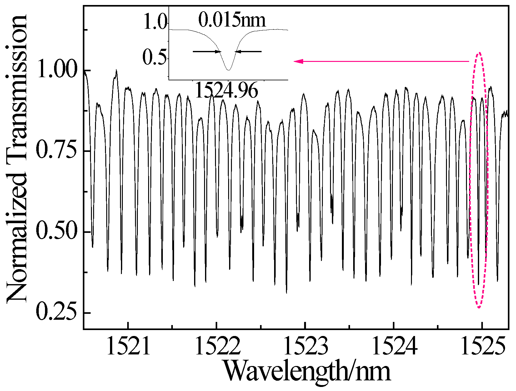
4. Results and Discussion

The resonance curves in the output and drop port of three different coupling regions are achieved through the test, and partial normalized transmission lines are shown in Figure 7 and Figure 8.
From the spectrums illustrated in Figure 7, it is apparent that the structure of concentric-coupled (a) achieves the deepest resonance depth and the strongest light intensity, but asymmetry of the spectral shape is obvious. The structure of straight-coupled (b) and butterfly-coupled (c), represent shallower resonant depth (c is slightly lighter than b), and both the spectrums become symmetric. This achieves a significantly sharper resonance valley and narrower 3 dB bandwidth, which are 0.133, 0.117 and 0.046 nm, respectively, corresponding to coupling modes a, b and c. Ultimately, the quality factors calculated at each output appear to be ~11,510 (a), ~12,750 (b) and ~33,270 (c).
Figure 7. Resonance spectrum of output ports.
Micromachines 06 00151 g007
Figure 8. Resonance spectrum of drop port in concentric-coupled.
Micromachines 06 00151 g008
The resonant spectrums are well consistent with the theoretical simulation in the second section. Phenomenon described above show that coupling ratios get larger with the increase of effective coupling length, thus causing higher light intensity and lower resonance point. Moreover, larger coupling coefficients make a wider 3 dB bandwidth, which is unfavorable for realization of a high-Q value.
It is worth noting that the resonance lines in the concentric-coupled drop port become disorganized and are even seriously lacking in 1535–1545 nm as shown in Figure 8. The increasing effective coupling length also makes it more likely for there to be a model mismatch, which causes more model mismatch loss, directly leading to the deterioration of the spectrums. At all events, it is the most undesirable phenomena in tests and applications of the optical cavities.
A large size resonator (642 μm-radius) with coupled waveguide (50 μm arc-radius) is designed in order to verify the advantage of the butterfly-coupled structure in improving resonant characteristics. Drop and add ports are designed in parallel in order to test expediently, and the designation will not influence the signal transmission in the two ports, because the bending of 180° is set after the coupling region. We have a good achievement of 3 dB bandwidth (0.015 nm) and a Q value as high as ~101,664. Scanning-electron-microscopy (SEM) and resonance lines are, respectively, represented, as shown in Figure 9 and Figure 10.
Figure 9. Scanning-electron-microscopy (SEM) of silicon-on-insulator (SOI) ring resonator.
Micromachines 06 00151 g009
Figure 10. Resonance lines of through port (R = 642 μm).
Micromachines 06 00151 g010

5. Conclusions

In summary, the coupling area of the SOI ring resonator is studied. Theoretical simulation and analysis are conducted to explore the relationships between the coupling length, coupling coefficient and quality factor. The coupling test shows that longer coupling length makes higher optical coupling strength and lower resonance point, while the 3 dB bandwidth is wider, which is not conducive to the realization of a high-Q and high sensitivity resonator. The large size ring resonator with Q factor of ten to the fifth power is achieved by adopting the butterfly-coupled form. An optimization design of coupling area for optical cavities to achieve the characteristics of high-Q value and high sensitivity undoubtedly has important research significance and application value for fields that have a strict need for quality factor; especially for the research in optical waveguide gyroscopes.

Acknowledgments

The project is supported by the National Natural Science Foundation of China (Grant Nos. 61275166, 91123036, 51225504, 61127008, 61178058), and the National High Technology Research and Development Programme (“863” Programme) of China (No. 2013AA041109). The authors thank the Suzhou Institute of Nano-Tech and Nano-Bionics of the Chinese Academy of Sciences for the contribution to the fabrication of the devices.

Author Contributions

Minghui Li and Shubin Yan made equal contributions to the research. Minghui Li and Shubin Yan made the theoretical analysis and designation of the structures, Liang Luo performed the simulations and Kezhen Ma carried out the coupling experiment. Prof. Dr. Chenyang Xue and Prof. Dr. Wendong Zhang supervised the work. Minghui Li wrote the main manuscript and all authors analyzed the results and reviewed the manuscript.

Conflicts of Interest

The authors declare no conflict of interest.

References

  1. Ma, H.; Wang, S.; Jin, Z. Silica waveguide ring resonators with multi-turn structure. Opt. Commun. 2008, 281, 2509–2512. [Google Scholar] [CrossRef]
  2. Yan, S.; Zhao, M.; Liu, Z.; Li, J.; Yan, Y.; Xue, C.; Liu, J. All-solid integrated optical waveguide Gyro based on chip. Infrared Laser Eng. 2011, 40, 921–925. [Google Scholar]
  3. Toland, J.R.E.; Search, C.P. Sagnac gyroscope using a two-dimensional array of coupled optical microresonators. Appl. Phys. B. 2014, 114, 333–339. [Google Scholar] [CrossRef]
  4. Shi, Z.; Shao, S.; Wang, Y. Improved the Surface Roughness of Silicon Nanophotonic Devices by Thermal Oxidation Method. J. Phys. Conf. Ser. 2011, 276, 012087. [Google Scholar] [CrossRef]
  5. Liang, E.Z.; Hung, S.C.; Hsieh, Y.P.; Lin, C.F. Effective energy densities in KrF excimer laser reformation as a sidewall smoothing technique. J. Vac. Sci. Technol. B. 2008, 26, 110–116. [Google Scholar] [CrossRef]
  6. Timotijevic, B.; Mashanovich, G.; Michaeli, A.; Cohen, O.; Passaro, V.M.N.; Crnjanski, J.; Reed, G.T. Tailoring the spectral response of add/drop single and multiple resonators in silicon-on-insulator. Chin. Opt. Lett. 2009, 7, 291–295. [Google Scholar] [CrossRef] [Green Version]
  7. Veerasubramanian, V.; Beaudin, G.; Giguère, A.; Drogoff, B.L.; Aimez, V.; Kirk, A.G. Waveguide-coupled drop filters on SOI using quarter-wave shifted sidewalled grating resonators. Opt. Express 2012, 20, 15983–15990. [Google Scholar] [CrossRef]
  8. Dong, P.; Feng, N.; Feng, D.; Qian, W.; Liang, H.; Lee, D.C.; Luff, B.J.; Banwell, T. GHz-bandwidth optical filters based on high-order silicon ring resonators. Opt. Express 2010, 8, 23784–23789. [Google Scholar] [CrossRef]
  9. Li, Y.; Zhang, L.; Song, M.; Zhang, B.; Yang, J.; Beausoleil, R.G.; Willner, A.E.; Dapkus, P.D. Coupled-ring-resonator-based silicon modulator for enhanced performance. Opt. Express 2008, 16, 13342–13348. [Google Scholar] [CrossRef] [PubMed]
  10. Jin, L.; Li, M.; He, J. Highly-sensitive silicon-on-insulator sensor based on two cascaded micro-ring resonators with vernier effect. Opt. Commun. 2010, 284, 156–159. [Google Scholar] [CrossRef]
  11. Faktorová, D.; Savin, A.; Grimberg, R. Enhancement of Waveguide Sensor for Biological Tissues Dielectric Properties Investigation with Metamaterials. In Proceedings of 2012 35th International Conference on Telecommunications and Signal Processing (TSP), Prague, Czech Republic, 3–4 July 2012; pp. 544–548.
  12. Kiyat, I.; Kocabas, C.; Aydinli, A. Integrated micro ring resonator displacement sensor for scanning probe Microscopies. J. Micromech. Microeng. 2004, 14, 374–381. [Google Scholar] [CrossRef]
  13. Delâge, A.; Xu, D.; McKinnon, R.; Post, E.; Waldron, P.; Lapointe, J.; Storey, C.; Densmore, A.; Janz, S.; Lamontagne, B.; Cheben, P.; Schmid, J. Wavelength-Dependent Model of a Ring Resonator Sensor Excited by a Directional Coupler. J. Lightwave Technol. 2009, 27, 1172–1180. [Google Scholar] [CrossRef]
  14. Rouger, N.; Chrostowski, L.; Vafaei, R. Temperature Effects on Silicon-on-Insulator (SOI) Racetrack Resonators: A Coupled Analytic and 2-D Finite Difference Approach. J. Lightwave Technol. 2010, 28, 1380–1391. [Google Scholar] [CrossRef]
  15. Xia, F.; Rooks, M.; Sekaric, L; Vlasov, Y. Ultra-compact high order ring resonator filters using submicron silicon photonic wires for on-chip optical interconnects. Opt. Express 2007, 15, 11934–11941. [Google Scholar] [CrossRef]

