Review

Femtosecond Laser 3D Fabrication in Porous Glass for Micro- and Nanofluidic Applications

State Key Laboratory of High Field Laser Physics, Shanghai Institute of Optics and Fine Mechanics, Chinese Academy of Sciences, P.O. Box 800-211, Shanghai 201800, China
*
Author to whom correspondence should be addressed.
Micromachines 2014, 5(4), 1106-1134; https://doi.org/10.3390/mi5041106
Submission received: 9 October 2014 / Revised: 22 October 2014 / Accepted: 22 October 2014 / Published: 17 November 2014
(This article belongs to the Special Issue Laser Micro- and Nano- Processing)

Abstract

:
The creation of complex three-dimensional (3D) fluidic systems composed of hollow micro- and nanostructures embedded in transparent substrates has attracted significant attention from both scientific and applied research communities. However, it is by now still a formidable challenge to build 3D micro- and nanofluidic structures with arbitrary configurations using conventional planar lithographic fabrication methods. As a direct and maskless fabrication technique, femtosecond laser micromachining provides a straightforward approach for high-precision, spatially-selective, modification inside transparent materials through nonlinear optical absorption. In this paper, we demonstrate rapid fabrication of high-aspect-ratio micro- and/or nanofluidic structures with various 3D configurations by femtosecond laser direct writing in porous glass substrates. Based on this approach, we demonstrate several functional micro- and nanofluidic devices including a 3D passive microfluidic mixer, a capillary electrophoresis (CE) analysis chip, and an integrated micro-nanofluidic system for single DNA analysis. The possible mechanisms behind the formation of high-aspect-ratio micro- and nanochannels are also discussed. This technology offers new opportunities to develop novel 3D micro-nanofluidic systems for a variety of lab-on-a-chip applications.

1. Introduction

Microfluidics is a rapidly emerging technology that enables miniaturization and integration for biological, chemical, and medical applications. Integration of fluidic functions such as valving, metering, mixing, transport, and separation on a single substrate has enabled construction of microfluidic systems that can control and manipulate tiny volumes of liquids with high precision, leading to downsizing of both chemical and biological analysis [1,2]. Most current microfluidic systems are primarily two-dimensional. Extension of these devices to three dimensions would allow for full integration of a broad range of different types of component and enable potential high-value applications. However, it is now still a challenge to realize complex three-dimensional (3D) microfluidic structures with current planar photolithography technologies, which require multilayer and multistep processing procedures to form 3D structures, including stacking, bonding, sealing, and so on.
Femtosecond laser direct writing is the main technique currently used to modify the interior of transparent materials in a spatially selective manner [3,4]. This is possible due to the nonlinear interaction between the tightly focused femtosecond laser beam and the transparent material since the interaction is effectively confined to the vicinity of focal point where the laser intensity exceeds the threshold for multiphoton absorption. For instance, femtosecond laser pulses have been used to write optical waveguides in both passive and active materials by locally modifying their refractive indices [5,6,7]. In combination with wet chemical etching, femtosecond laser direct writing has also been used to fabricate microfluidic structures, including microchannels and chambers [8,9], microvalves [10], and micropumps [11]. The same technique has been extended to fabricate free-space optics such as micromirrors and micro-optical lenses in glass materials [12,13,14]. By virtue of its unique ability to build different types of functional components into a monolithic glass substrate, femtosecond laser direct writing offers a flexible approach to fabricate a wide variety of integrated microsystems and devices such as microfluidic lasers [15], optofluidic sensors [16,17,18,19,20,21], micro-electrodes [22,23,24,25,26] and micro-mechanics [27,28].
Currently, there are mainly two strategies for fabricating 3D microfluidic channels embedded in glasses using a femtosecond laser. The first strategy employs femtosecond laser modification inside glass materials followed by chemical wet etching [29,30,31]. Unfortunately, with this technique the length of the microfluidic channel that can be fabricated is usually limited to a few millimeters, due to the limited etch ratio between the areas with and without the femtosecond irradiation. Another strategy is to perform femtosecond laser 3D drilling from the rear surface of the glass in contact with distilled water, in which the water introduced into the microchannel can help to remove the ablated debris [32]. However, when the length of the channel increases, the debris can no longer be ejected from the microchannel, which in turn causes clogging and termination of the microchannel. So far, the microchannels fabricated by these methods often suffer from their insufficient lengths for practical microfluidic applications.
Another challenge of fabricating 3D fluidic structures by femtosecond laser direct writing is the limited fabrication resolution mainly caused by the optical diffraction limit. So far, by inducing two-photon polymerization (2PP) of photosensitive materials with femtosecond laser pulses, 3D fabrication with a resolution of sub-100 nm has already been achieved by choosing laser intensity slightly above a threshold value [33]. However, the 2PP technology is intrinsically limited to polymer materials, in which direct formation of thin microfluidic channels cannot be easily achieved due to the difficulty in removing the non-photopolymerized materials contained in the thin channels. Currently, the thinnest microfluidic channels were obtained by liquid-assisted femtosecond laser 3D drilling, resulting in channel diameters ranging from 500 to 700 nm [34].
This review article focuses primarily on our recent efforts to tackle the two issues as mentioned above. By use of femtosecond laser direct writing in porous glass immersed in water followed by post-annealing, we demonstrated microfluidic channels with nearly unlimited lengths and arbitrary 3D geometries [35,36]. By controlling the laser peak intensity and polarization, a single nanocrack with sub-50-nm feature size could be achieved inside porous glass [37]. Based on these strategies, several functional devices and their applications are demonstrated, including large-volume hollow chamber [38], 3D passive microfluidic mixer [39], capillary electrophoresis (CE) analysis chip [40], and an integrated micro-nanofluidic system for single DNA analysis [41]. The possible mechanisms behind the formation of a single nanochannel are also discussed [42,43]. Finally, future opportunities and current challenges for this novel approach are highlighted.

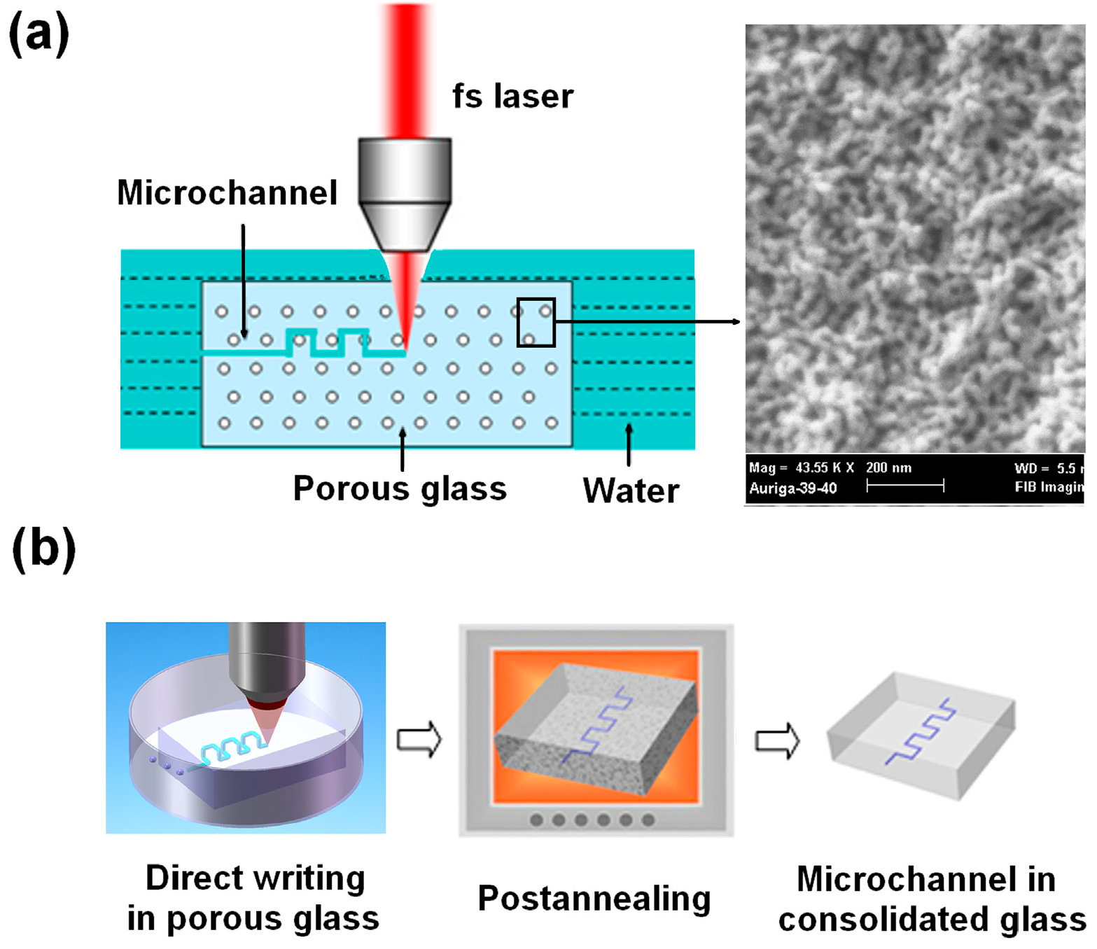
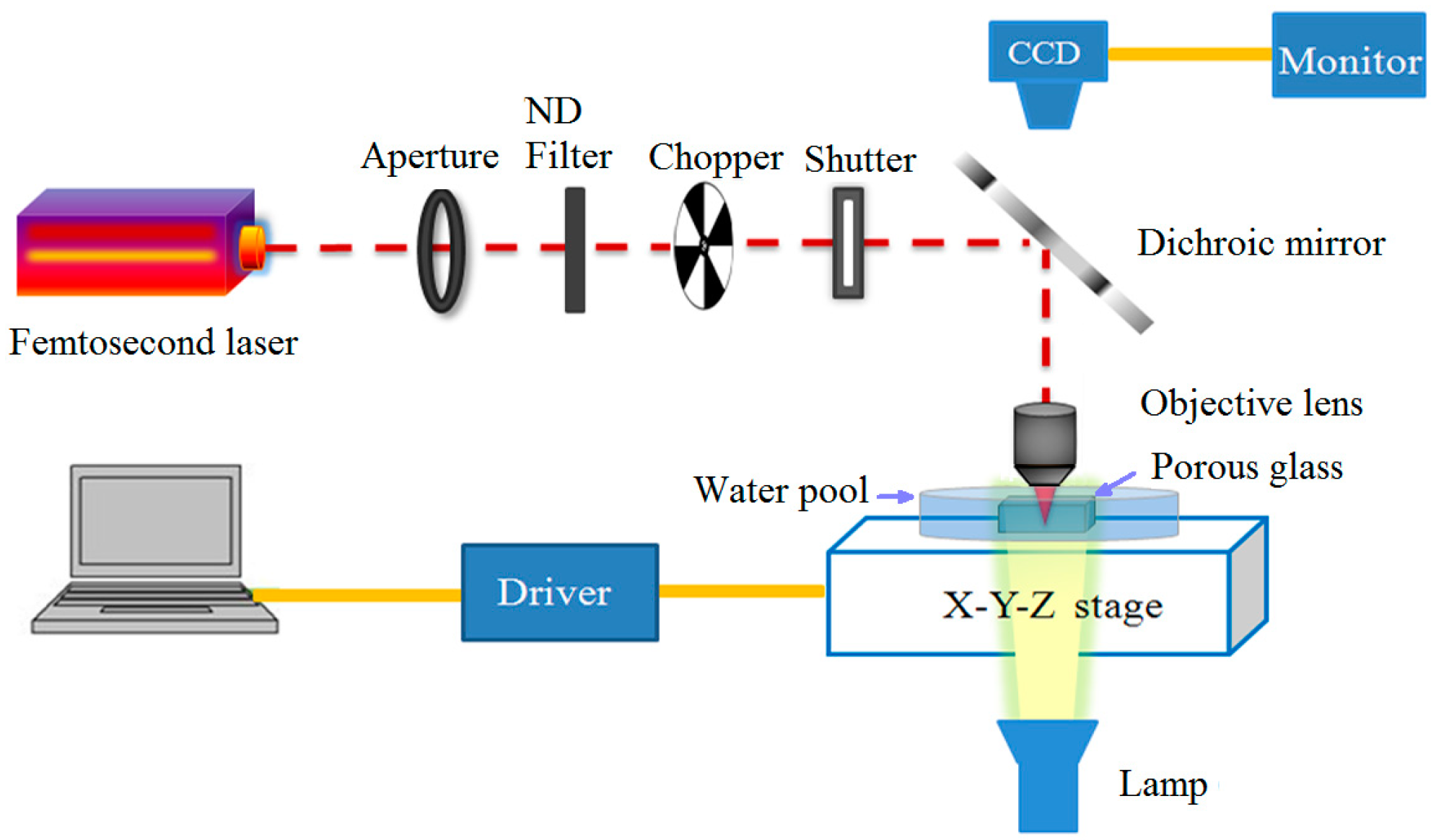
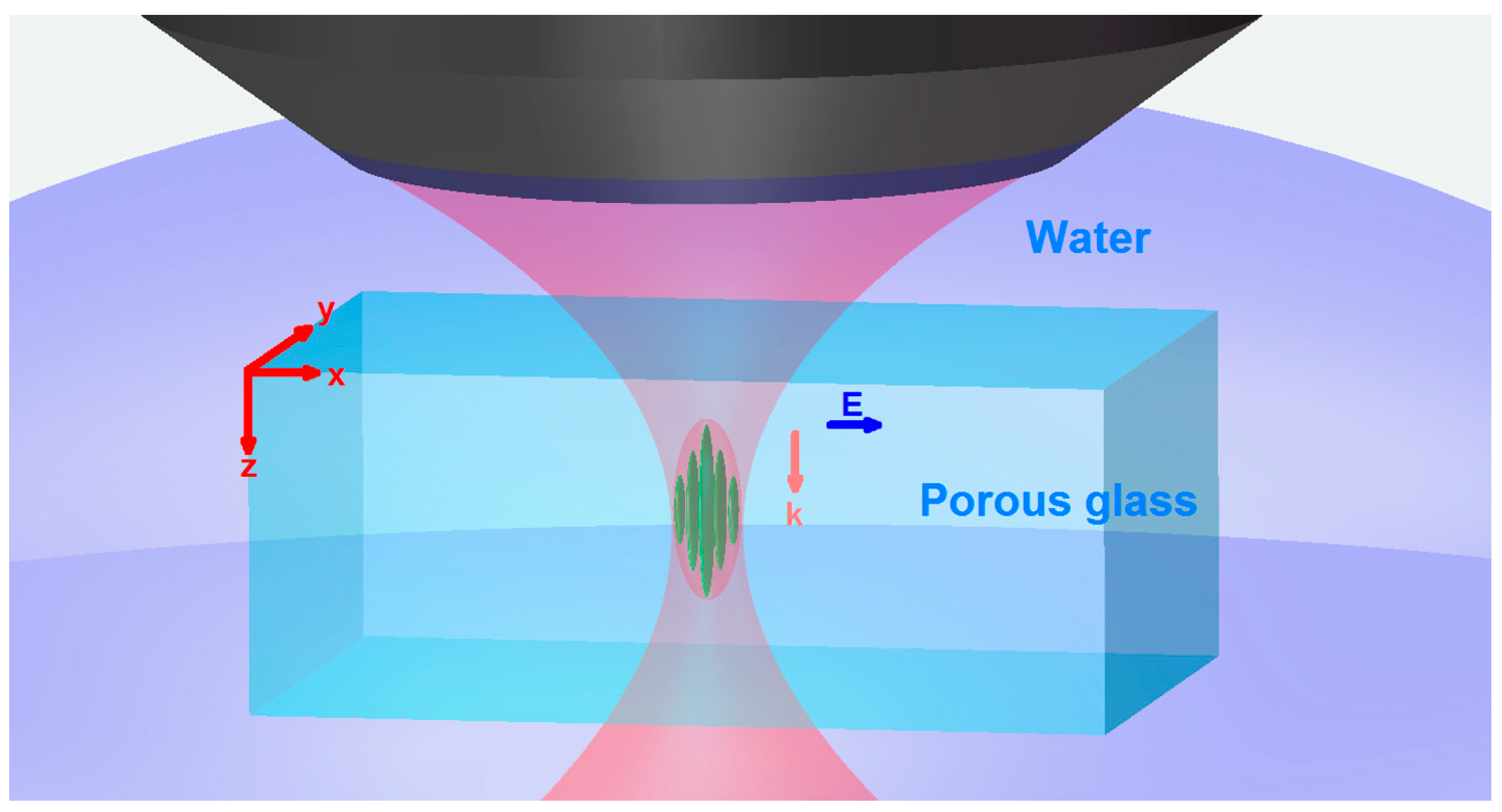
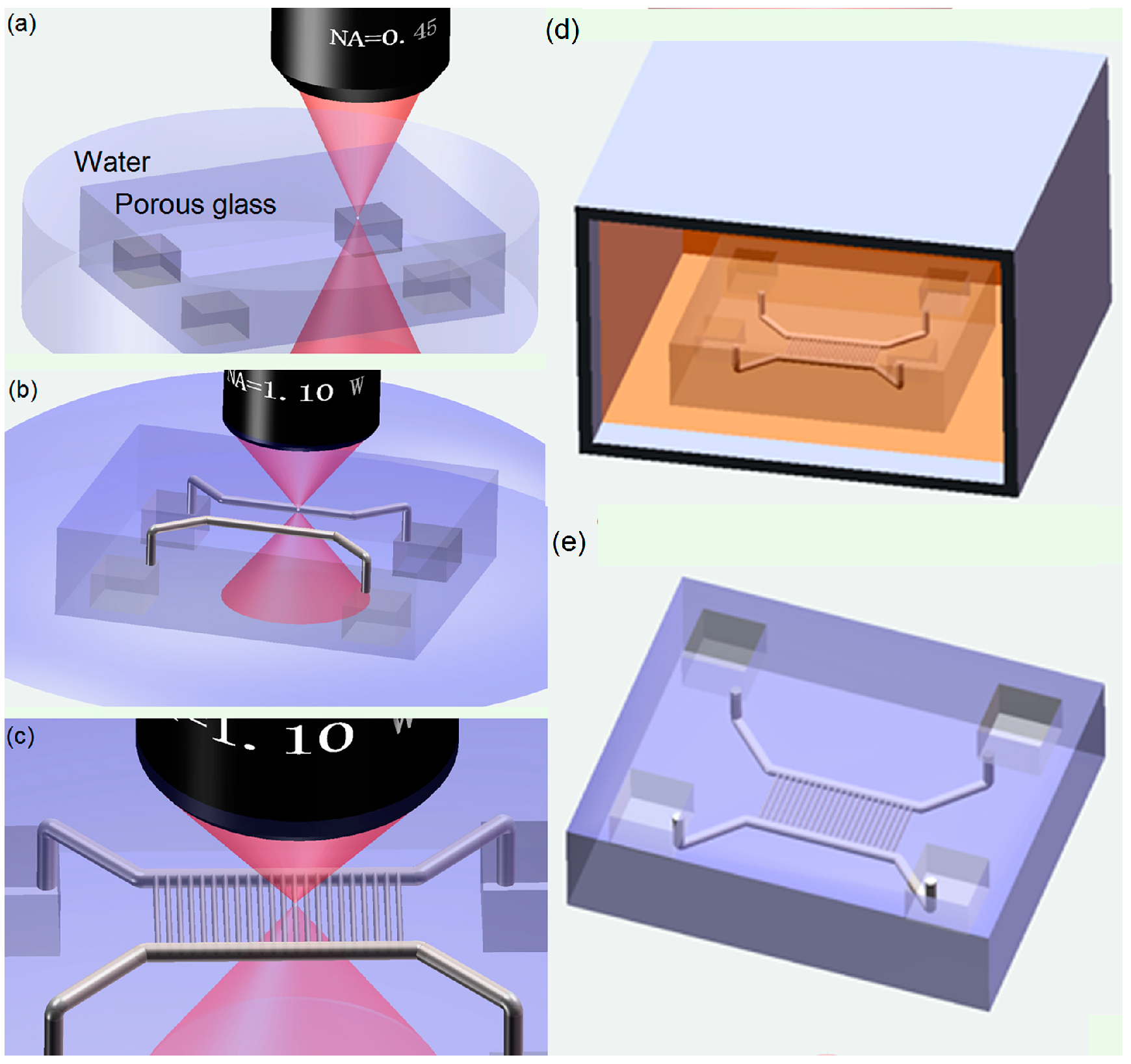
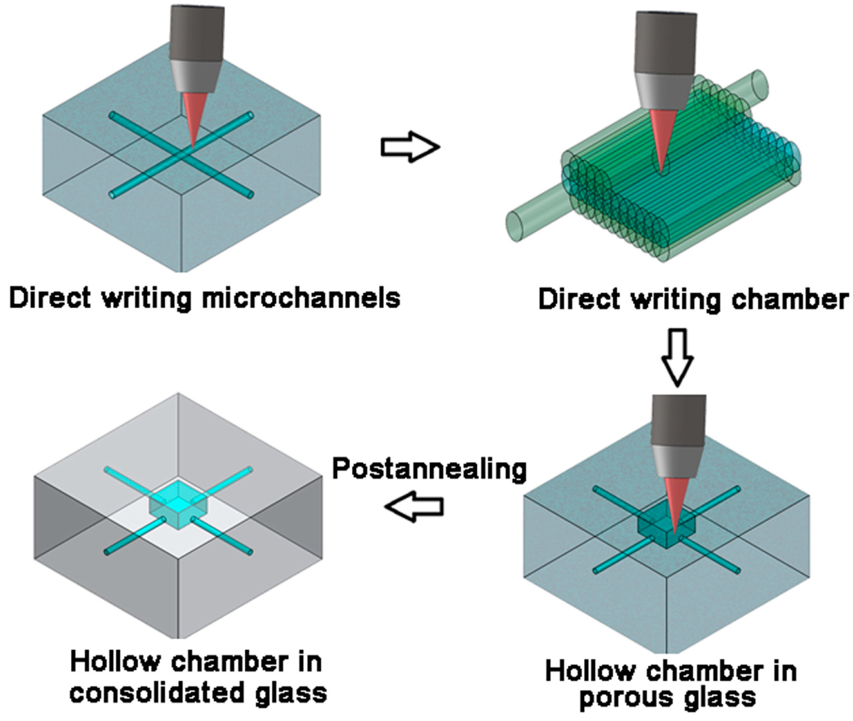
2. Experimental Setup and Fabrication Process

In this work, a high-silica porous glass was used as a substrate, which was produced by removing the borate phase from phase-separated alkali-borosilicate glass in hot acid solution [44]. The composition of the porous glass is approximately 95.5 SiO2-4 B2O3-0.5 Na2O (wt %). The pores with a mean size of ~10 nm are distributed uniformly in the glass and occupy 40% volume of the glass. Particularly, these pores in the porous glass form a 3D connective network, which allows liquid to flow through.
Figure 1 schematically shows a typical experimental setup used for femtosecond laser direct writing in porous glass, which consists of a femtosecond laser amplifier system (Coherent, Inc., Santa Clara, CA, USA, center wavelength: ~800 nm, pulse width: ~50 fs, repetition rate: 1 kHz ~250 kHz), a Charge-coupled Device (CCD) imaging system, a computer-controlled XYZ translation stage, beam control devices and delivery optics. The Gaussian laser beam with an initial 8.8 mm diameter was passed through a ~3 mm-diameter aperture for ensuring a high beam quality (i.e., only the central part of the beam was used because of its high homogeneity). A long-working-distance water-immersed objective was employed for focusing the beam into the porous glass sample, which was fixed in a petri dish filled with distilled water. The petri dish was placed on the translation stage, as shown in Figure 1. Since the high-repetition-rate laser pulses could also lead to temporary evacuation of water in the laser action zone by semi-continuous irradiation, a chopper was used to modulate the femtosecond laser pulse train during the ablation process, so that the water can always fill the ablation zone by infiltration through the porous network.
Figure 1. Schematic of the setup used for femtosecond laser direct writing in porous glass.
Micromachines 05 01106 g001
Figure 2a,b shows the schematic view of the experimental setup and the flow diagram for the fabrication process, respectively. The main fabrication process includes two steps: (1) direct formation of 3D microchannels from one side of a porous glass substrate immersed in water by femtosecond laser direct writing and (2) postannealing of the glass substrate at ~1150 °C by which the porous glass can be consolidated. The inset scanning electron microscope (SEM) image in Figure 2a clearly shows the size distributions of nanopores are homogeneous. After the consolidation process, all the nanopores in the porous glass disappeared; however, the fabricated microchannels could survive due to their large diameter. Moreover, the porous structure is consolidated into a clear impervious glass known as Vycor brand 96% SiO2 glass, which is similar to fused silica in its thermal properties and light transmittance [44].
Figure 2. (a) Schematic view of experimental setup. (b) Flow diagram for the fabrication process.
Micromachines 05 01106 g002

3. Laser Direct Writing of Microchannels

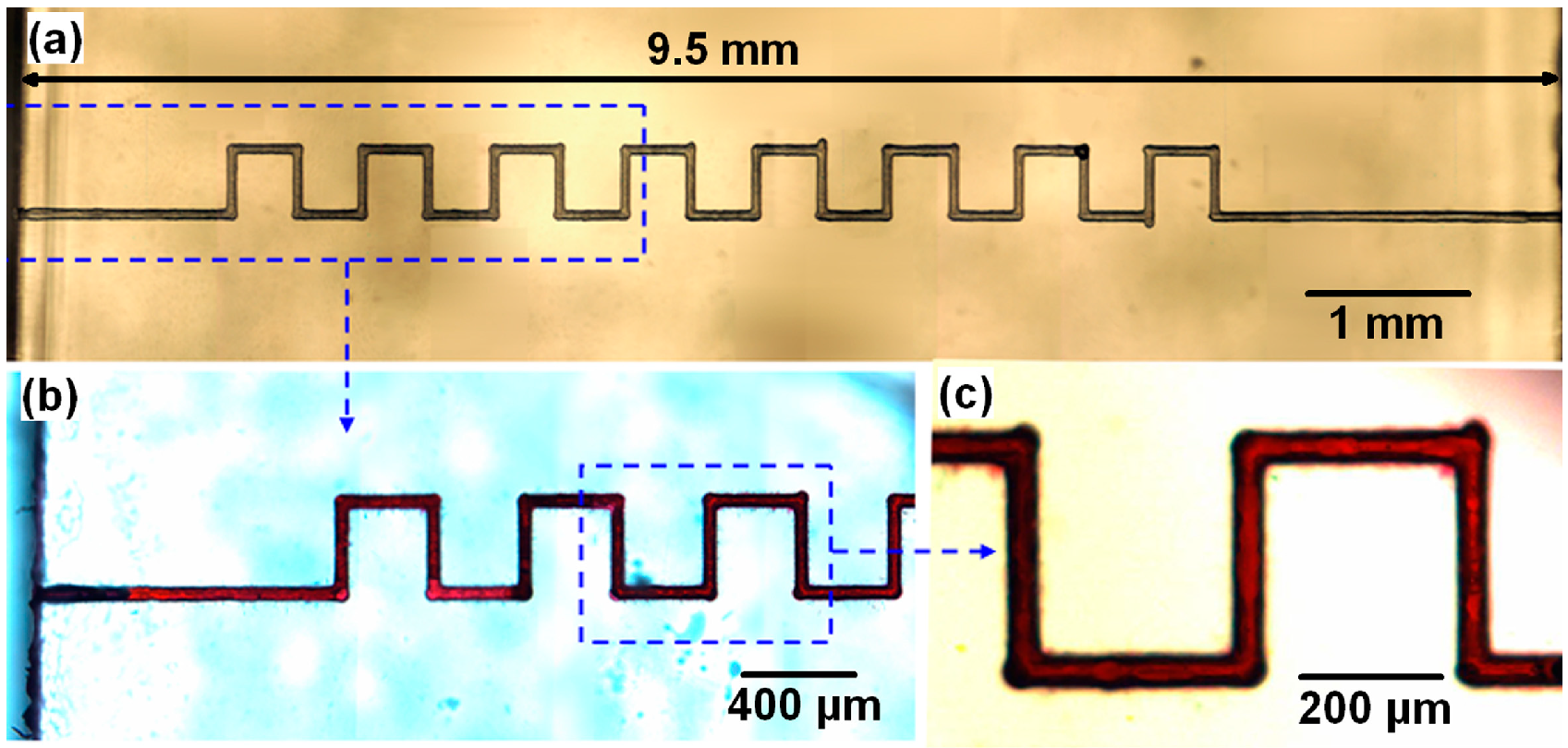
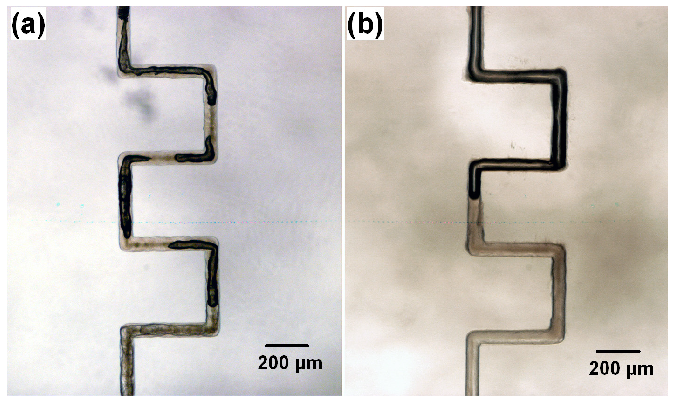
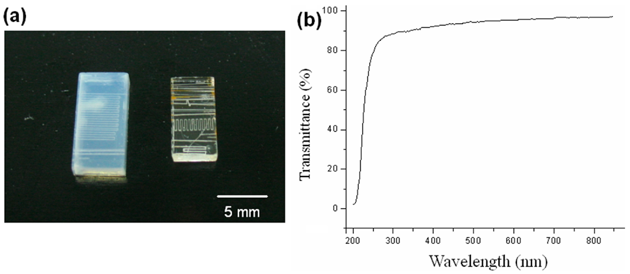
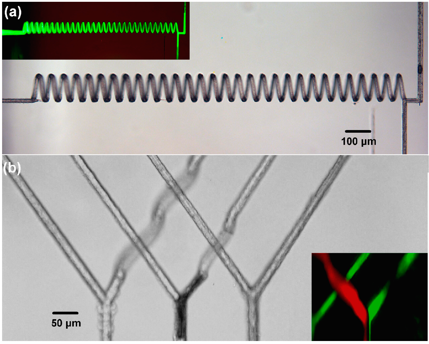
3.1. Fabrication of Multi-Centimeter-Long Microchannels

For laser direct writing of microchannels in porous glass, relatively high laser intensity is required for inducing laser ablation in microchannel. Typically, a 50× objective (numerical aperture (N.A.) = 0.80) was employed for focusing the 1 kHz femtosecond laser pulses at a depth of 300 μm below the sample surface. The laser pulse energy was chosen to be 60 μJ, and the translating speed was set to be 20 μm/s. Figure 3a shows a section of microchannel inside porous glass immersed in water, wherein the dark segments consisted of gas bubbles produced when focusing femtosecond laser pulses on the silica/water interface. The discontinuous bubble segments indicate that some parts of the channel were blocked by debris created by laser ablation. By repeatedly scanning, the water could disperse and flush away clogged segments, until a homogeneous and continuous hollow channel was obtained. The continuous bubble section shown in Figure 3b indicates that the channel is homogeneous and debris-free, after one slow scan at 20 μm/s followed by repeatedly scanning the whole microfluidic channel six times at a higher translation speed of 1 mm/s.
Figure 4a shows a top view micrograph of the homogeneous square-wave-like microchannel embedded in porous glass with a total length of ~1.6 cm, which was obtained by multiple scans with a total machining time of ~15 min. However, the microfluidic channel embedded in porous glass cannot be directly used for microfluidic application, because the liquid in the channel tends to permeate into the surrounding pores. To collapse all the pores, the sample was further annealed at 1150 °C for 1 h. Figure 4b,c shows optical micrographs of the postannealed microchannel filled with red ink. It is clear that the ink is well confined in the microchannel, which indicates that the microchannel is completely sealed because the pores have been closed after postannealing.
It should be specifically mentioned that after the consolidation process, the glass substrate shrinks in all the three directions. The initial length of ~1.6 cm of the microfluidic channel decreases to ~1.4 cm after the postannealing. Furthermore, we compare the cross sections of microchannels before and after the postannealing by breaking up the microfluidic channels, as shown in Figure 5a,b. Table 1 gives geometric sizes of microchannel before and after annealing, which indicate the shrinkage factors in three directions are almost equal. The corresponding volume shrinkage factor is ~39%, approximately equal to the 40 vol % porosity of porous glass. Note that there are some cracks along the laser propagating direction around the microchannels as shown in Figure 5a,b, which could result from inhomogeneous axial intensity distribution of the incident laser due to both self-focusing effect and spherical aberration effect [45].
Figure 3. Optical micrographs of microchannels in porous glass fabricated by (a) single scan and (b) multiple scans.
Micromachines 05 01106 g003
Figure 4. (a) Optical micrograph of a 1.6-cm-long microchannel embedded in porous glass before postannealing. (b) Optical micrograph of postannealed microchannel filled with red ink. (c) Close-up view of (b) [35] (Reproduced with permission from OSA. ©2010 by the Optical Society of America).
Micromachines 05 01106 g004
Figure 5. Cross-sectional views of the cleaved microchannel (a) before and (b) after the postannealing [35] (Reproduced with permission from OSA. ©2010 by the Optical Society of America).
Micromachines 05 01106 g005
Table 1. Geometric sizes of microchannel before and after annealing.
DescriptionCross section size (transverse)Cross section size (vertical)Channel length
Before annealing74 μm114 μm9.50 mm
After annealing63 μm97 μm8.00 mm
Shrinkage factor14.9%14.9%15.8%
Moreover, the porous glass substrate, which is opaque due to the scattering of the nanopores, becomes highly transparent after the consolidation process, as shown in Figure 6a. Figure 6b gives a transmission spectrum of the consolidated glass, which shows superior transmission ranging from ultraviolet radiation (UV) to the near infrared radiation (IR). This facilitates the future incorporation of optical functions in the glass for optofluidic applications.
Figure 6. (a) The porous glass before (left) and after (right) postannealing. (b) Transmission spectrum of the consolidated glass.
Micromachines 05 01106 g006

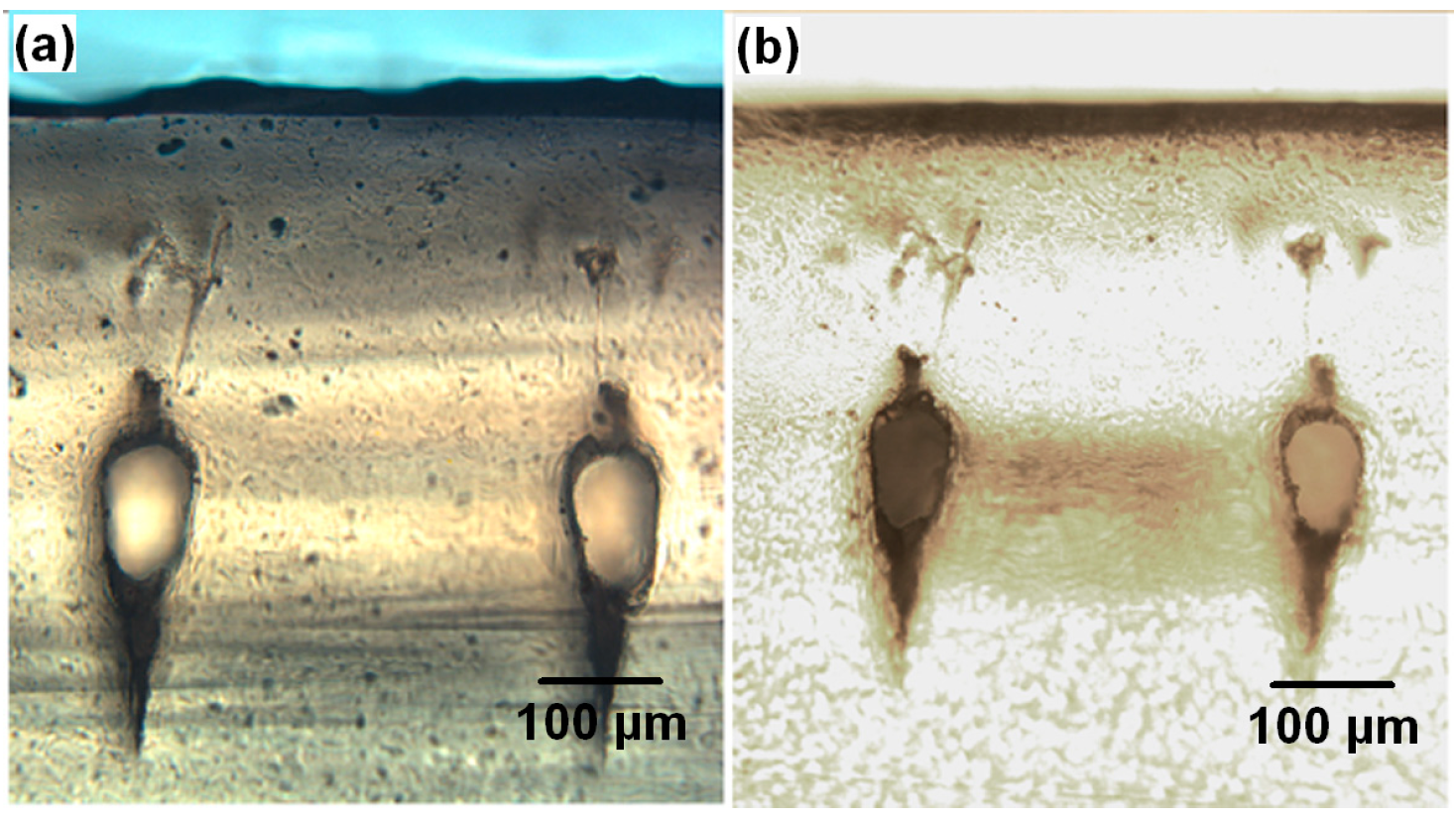
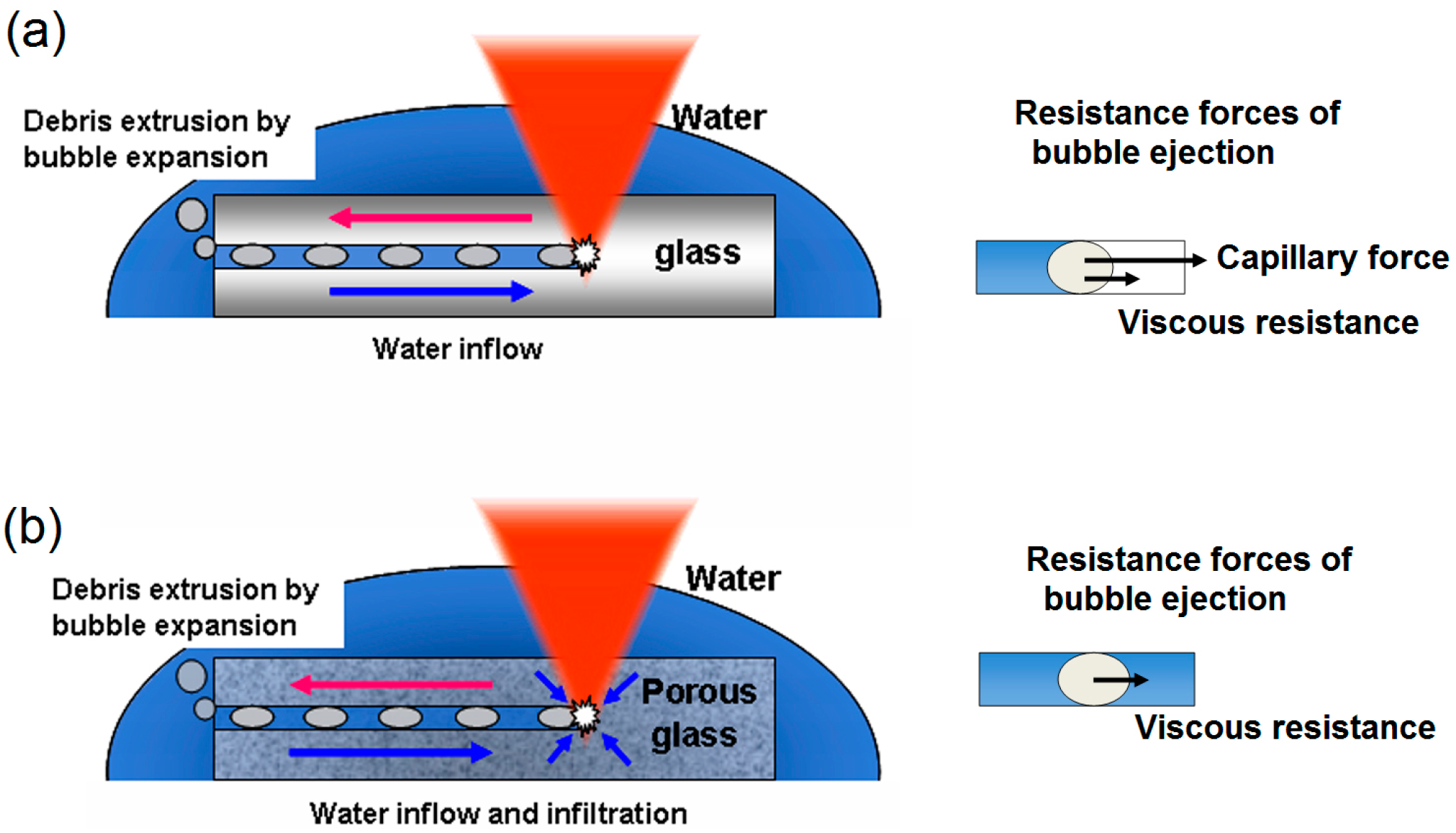
3.2. Mechanism of Efficient Removal of Debris

In this section, we discuss the dominant mechanism that is responsible for the removal of debris from the microchannel during the femtosecond laser direct writing in porous glass. Actually, in the previous studies of fabrication of microfluidic channel in fused silica by water-assisted femtosecond laser drilling [32,46], it has been observed that the drilling process relies heavily on water circulation in the microchannel, which is a bi-directional mass transfer process including both the water flowing into laser ablation zone from the inlet of mcirochannel driven by capillary force and bubbles ejecting through the inlet driven by the shock wave produced by the femtosecond laser, as schematically shown in Figure 7a. The water mainly plays two key roles for producing hollow structures: (1) dispersing the debris produced by laser ablation; and (2) producing bubbles to expel the debris from the channel through the inlet, which in return promotes the water circulation. Unfortunately, as the length of channel increases in solid glass, once the bubble and debris build up to the extent that water inflow is blocked, the drilling process will terminate. However, for porous glass, the water can continuously infiltrate into the ablation zone through the porous network, as schematically shown in Figure 7b, even if the microchannel is blocked. Therefore, the repeated back and forth writing can always disperse debris and produce bubbles independent of the length of microchannel.
In the right panels of Figure 7a,b, the resistance forces of bubble ejection when microchannel is blocked by bubbles are illustrated for solid glass case and porous glass case, respectively. For porous glass case, it will be much easier to drive the bubbles out from the channel because the capillary force exerted by water surrounding bubbles is balanced out. In our experiment of femtosecond laser direct writing in porous glass, somewhere the microchannel could be temporarily blocked if some of the bubbles in the channel do not have enough time to escape from the channel before the new debris is produced. However, we can easily expel the bubbles from the channel by scanning the femtosecond laser beam along the channel repeatedly.
In addition, due to the porosity of the sample, the amount of debris produced by the femtosecond laser ablation would be less than that in the traditional water-assisted drilling inside dense glass. Furthermore, the porosity of the sample will also allow for directly creation of hollow space by localized solidification and the collapse of the nanopores, which has been verified by the formation of hollow nanogratings in porous glass [37].
Figure 7. Schematic illustration of water-assisted direct-writing process in (a) solid glass and (b) porous glass.
Micromachines 05 01106 g007

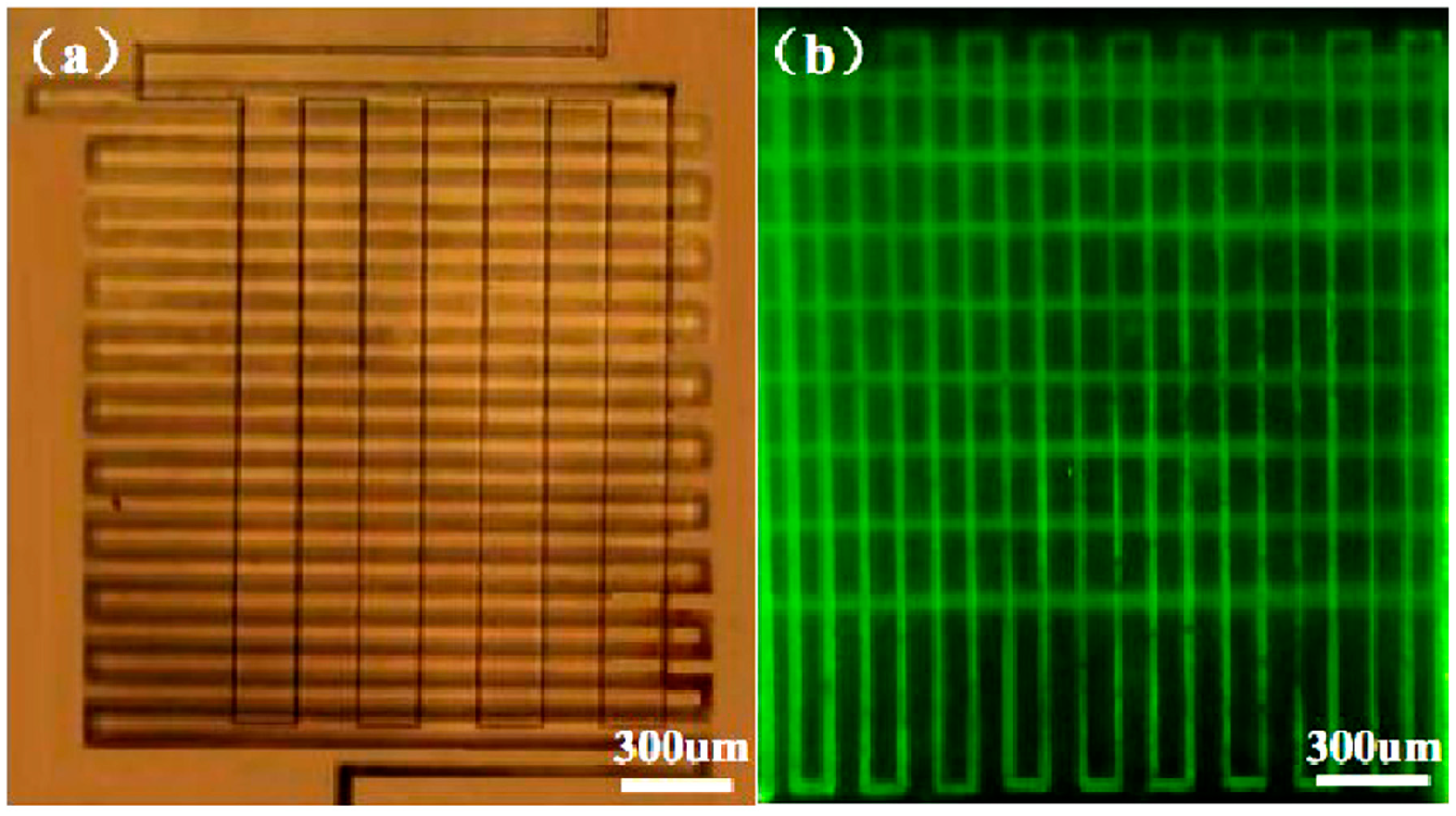
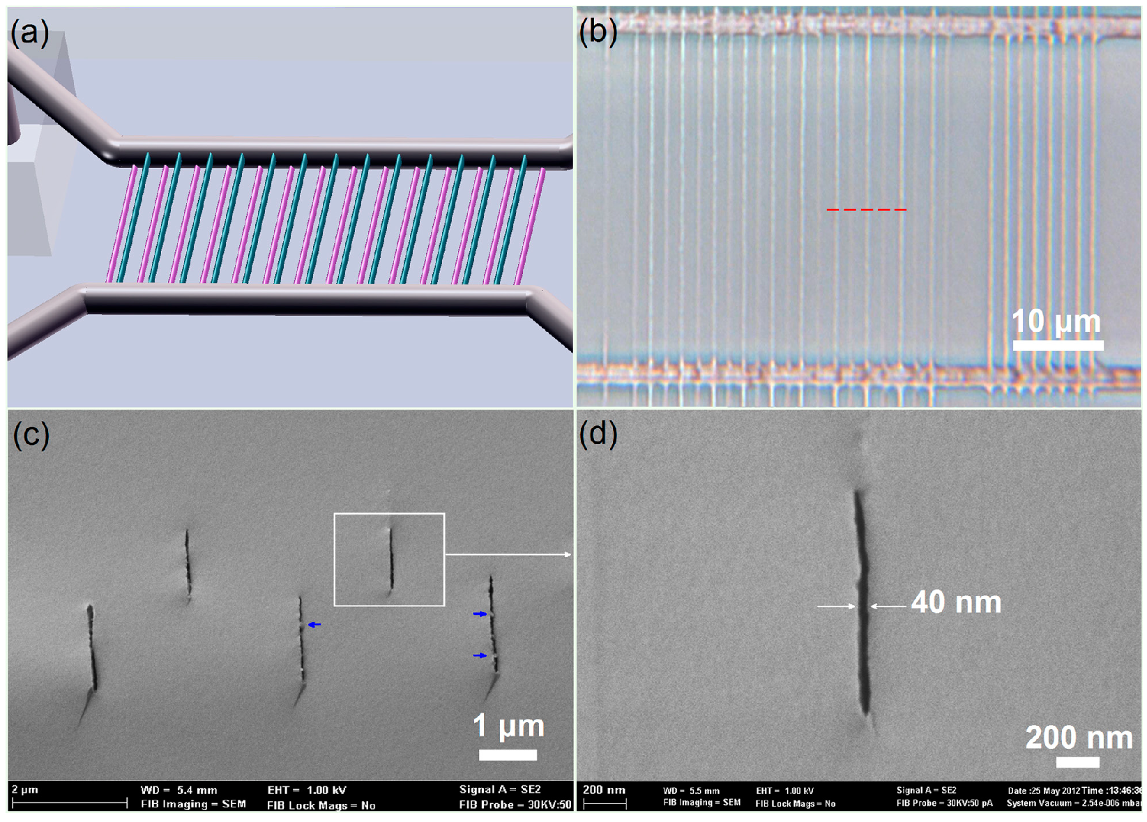
3.3. High-Aspect-Ratio 3D Microchannels

For direct writing of high-aspect-ratio (length-to-diameter) microchannels, both high-repetition-rate femtosecond laser pulses and tightly focusing are desirable. Here, the 250-kHz femtosecond laser pulses with a pulse energy of ~2 μJ were tightly focused by a water-immersed objective (N.A. = 1.0). Under such conditions, a peak laser intensity of ~8 × 10¹⁵ W/cm2 can be reached in a tiny focal volume with a diameter of ~0.8 μm, which is sufficiently strong for inducing nonlinear optical absorption and ablation of the glass material. The significant amount of heat and strong shock waves generated by the femtosecond laser ablation can facilitate water circulation and help to remove the debris from the outlet of the microchannel. Since the high-repetition-rate laser pulses could also lead to temporary evacuation of water in the laser action zone by semi-continuous irradiation, a chopper operated at 1 kHz with a duty of 50/50 was used (see Figure 1) to modulate the femtosecond laser pulse train during the ablation process, so that the water can always fill the ablation zone by infiltration through the mesoporous network [47].
The 3D nature of the femtosecond laser direct writing offers unique flexibility for constructing complex microfluidic networks [48]. Figure 8a shows a 3D helical microchannel with a total length of ~1 cm and a diameter of ~16 μm (i.e., corresponding to an aspect ratio of >600). The coil radius and the pitch of the helical channel are 100 μm and 50 μm, respectively. The homogeneous and debris-free helical channel was produced inside porous glass by performing one slow scan (10 μm/s) followed by three fast scans (100 μm/s) over the whole microfluidic channel. The total fabrication time is less than 30 min. Figure 8b shows several overpass structures consisted of spiral-like bends along microfluidic channels, by which one microchannel can cross over the others. The fluorescence micrograph presented in the inset of Figure 8b indicates that indeed, the two microchannels do not intersect each other. The insets in Figure 8a,b presents fluorescence microscopy images of the fabricated microchannels filled with fluorescein solutions. The confined fluorescent solution gives proof that nanopores have all collapsed to form the consolidated substrate.
Many microfluidic applications such as electrophoresis require long channels compactly deployed in a tiny space. Compact microfluidic systems not only reduce the sizes of micro-analysis systems but also promote device performances such as sensitivity. Toward this goal, we fabricated a 3D two-layer microfluidic channel structure in porous glass with a length up to ~6.6 cm. Such a channel length can be sufficient for electrophoresis-based chemical analysis [49,50]. Figure 9a,b shows a microchannel with an aspect ratio of ~5500 fabricated in porous glass and consolidated glass, respectively. The total length of the microchannel is 6.6 cm and its diameter is ~12 μm, and the distance between the two layers was ~30 μm. In this case, femtosecond laser pulses with a pulse energy of ~3.5 μJ were tightly focused into porous glass substrate using a water-immersed objective (N.A. = 1.0). The debris-free microchannel was written back and forth at a low translation speed, and the total fabrication time is ~3 h. To our knowledge, this is so far the longest microfluidic channel with the highest aspect ratio produced in a glass substrate by femtosecond laser direct writing. In fact, there is no limit on the channel length with this technique if one would spend enough time on fabrication of the structure.
Figure 8. Optical micrographs of (a) a 3D helical microchannel and (b) 3D microfluidic channels crossing over each other embedded in consolidated glass, Insets: Fluorescence microscopy image of the microchannel filled with fluorescein solutions [39] (Reproduced with permission from RSC. ©2012 by the Royal Society of Chemistry).
Micromachines 05 01106 g008
Figure 9. (a) Optical micrograph of a two-layer microfluidic channel in porous glass with a length up to 6.6 cm. (b) Fluorescence microscopy image of the postannealed microchannel filled with a solution of fluorescein.
Micromachines 05 01106 g009

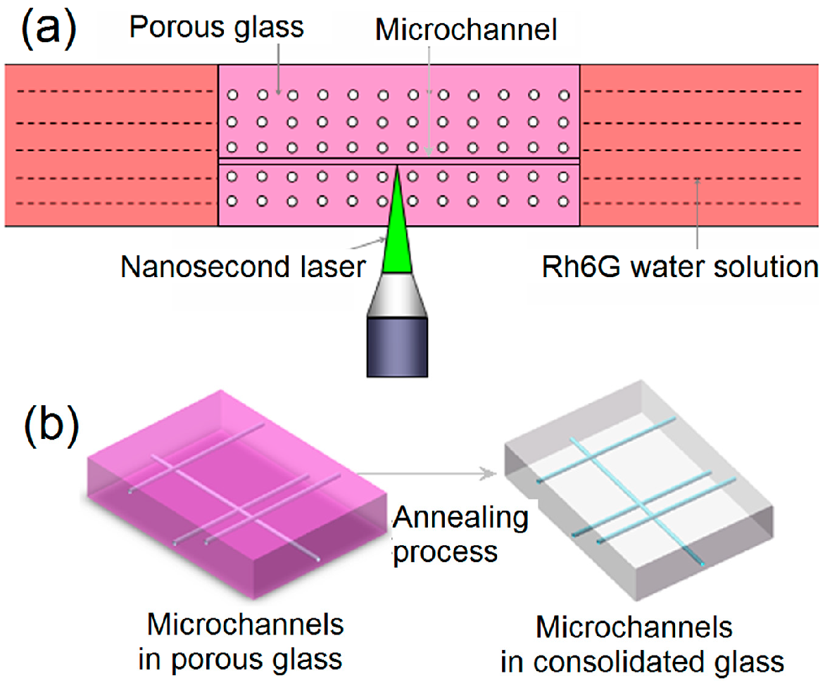
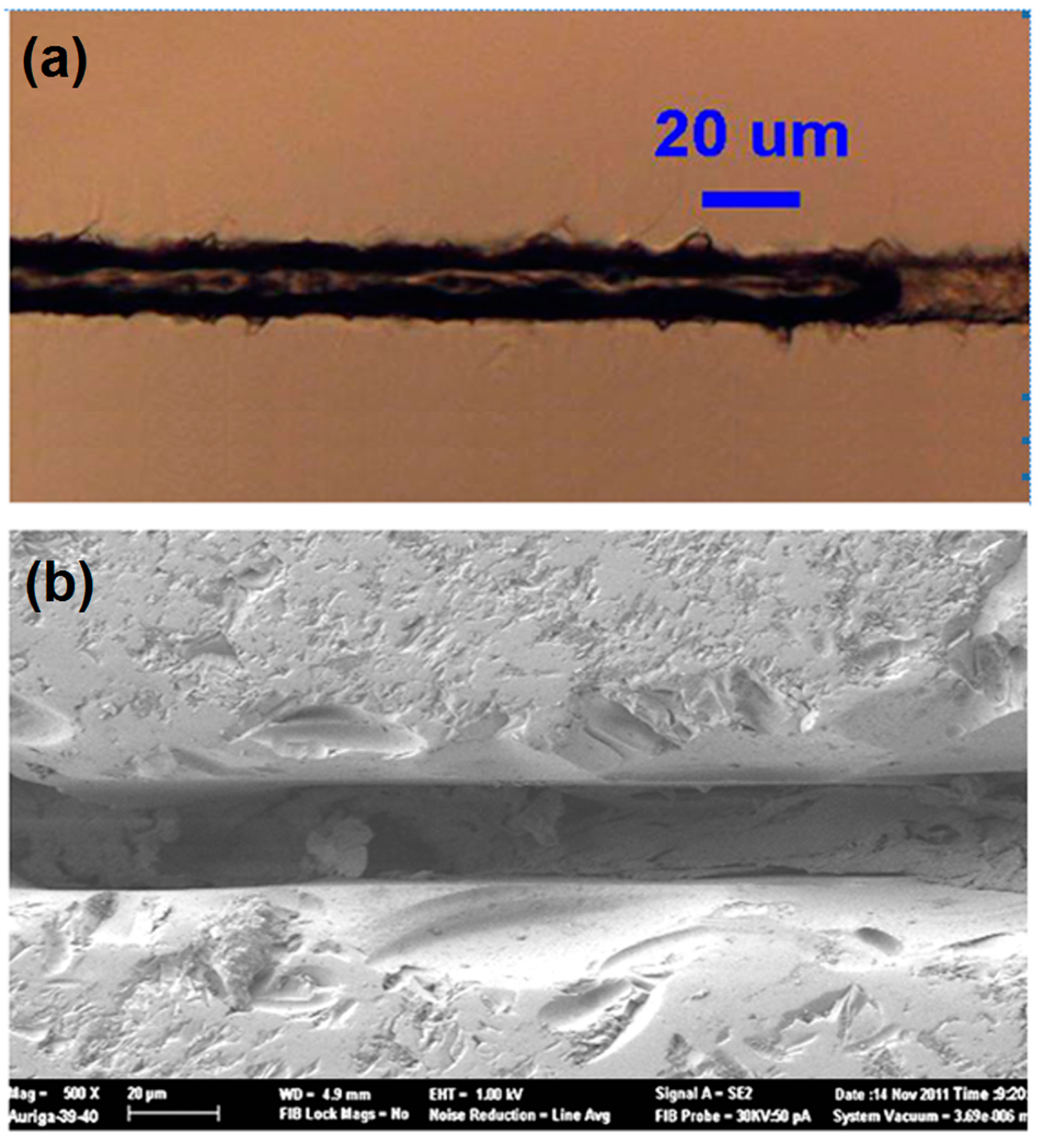
3.4. Microchannels Fabricated by Nanosecond Laser

Despite the rapid development of ultrafast laser technology in recent years, femtosecond laser systems are still expensive and difficult to operate as compared to other types of lasers, hampering their applications in industrial environment. In this section, we show that 3D microchannels can also be fabricated in porous glass using a Q-switched, frequency-doubled Nd:YAG laser [51]. The processing mainly consists of two steps: (1) formation of hollow microfluidic channels in porous glass immersed in Rhodamine 6G (Rh6G) dissolved in water by nanosecond laser ablation; and (2) postannealing of the fabricated porous glass sample at 1120 °C for consolidation of the sample. Here, Rh6G plays an important role as an absorber for promoting the ablation by the nanosecond laser within the porous glass sample, e.g., near the focal volume. The mechanism behind this technique is somewhat similar to that of laser induced backside-wet etching (LIBWE) [52,53,54], in which glass surface in contact with organic solution can be ablated by nanosecond laser to form surface microstructures. Due to the fact that the porous glass is immersed in a solution doped with Rh6G, the liquid can penetrate into the substrate through the nanopores. Since we use a 532 nm laser whose wavelength is close to the absorption peak of Rh6G (~520 nm), we choose the Rh6G in water for achieving an efficient absorption at the focus. Therefore, ablation inside glass is possible. Although the nanosecond laser could result in relatively low fabrication resolution due to its associated heat effect, there is no doubt that replacing the femtosecond laser by the nanosecond laser will greatly reduce the cost for fabricating 3D microfluidic devices whereas in the meantime enhance the stability of the laser source.
Figure 10a shows a schematic illustration of the system for carrying out nanosecond laser direct writing in porous glass immersed in Rh6G diluted with water at a concentration of C = 6.0 × 10⁻³ mol/L. Before being immersed in the liquid, the porous glass appears opaque due to the strong scattering of light from the nanopores; however, after soaked in the liquid, because of the smaller refractive-index difference between the glass (n = 1.46) and the absorbing liquid (n = 1.33) as compared to the refractive-index difference between the glass and air (n = 1), the scattering of light can be significantly reduced, which facilitates formation of high-quality focal spot inside glass. The laser was operated at a wavelength of 532 nm with 10 ns pulse duration (Full width at half maximum (FWHM)) and a repetition rate of 10 Hz. The incident pulse energy was chosen to be ~100 μJ. The nanosecond laser beam was focused into the porous glass through an objective lens (N.A. = 0.8). Some straight microfluidic channels were fabricated inside the porous sample at different depth as illustrated in Figure 10b.
Figure 10. (a) Schematic view of experimental setup and (b) flow chart for the whole fabrication process [51] (Reproduced with permission from OSA. ©2012 by the Optical Society of America).
Micromachines 05 01106 g010
The microchannels were fabricated by a single scan at a translation speed of 10 μm/s until the desired length is achieved, followed by several back-and-forth scans at a translation speed of 100 μm/s for completely removing the debris remaining in the channel. Uniform channels of a total length up to ~1 cm were achieved after the multiple scan. The total process for fabricating the 1-cm-long channel took ~1 h, limited by the low repetition rate of our YAG laser. After the laser direct writing, a post-annealing process was applied to the sample for collapsing all the nanopores in the glass, so that leak-free microfluidic channels are formed. The temperature inside the furnace was ramped up to 1120 °C at a rate of 1 °C/min and held at 1120 °C for 2 h and then naturally cooled down to room temperature. Before the post-annealing, the sample was soaked in acetone to take an ultrasonic bath for 30 min for removing the Rh6G molecules. A small amount of residual Rh6G dye left behind by the ultrasonic bath was further completely removed during the postannealing.
Figure 11a shows a top view optical micrograph of a machined microfluidic channel embedded in porous glass before post-annealing. The left section of the channel was empty and thus appeared dark, while the right section was filled with liquid and then appeared bright. In order to examine the morphology of the innerwall of microchannel, we polished the sample from the top surface until the microchannel was exposed. A SEM image of the surface morphology of the postannealed sample is shown in Figure 11b. It is clear that the innerwalls of the channel after the postannealing process show relatively high surface roughness, which can be attributed to the debris redeposited onto the inner wall of the microchannel. The debris possibly could be reduced or even totally removed by an additional chemical etching in diluted hydrofluoric acid (HF).
Figure 11. (a) Top view optical micrograph of a machined channel embedded in porous glass before postannealing. (b) SEM image of the innerwall of the channel after postannealing.
Micromachines 05 01106 g011

4. 3D Microfluidic Devices

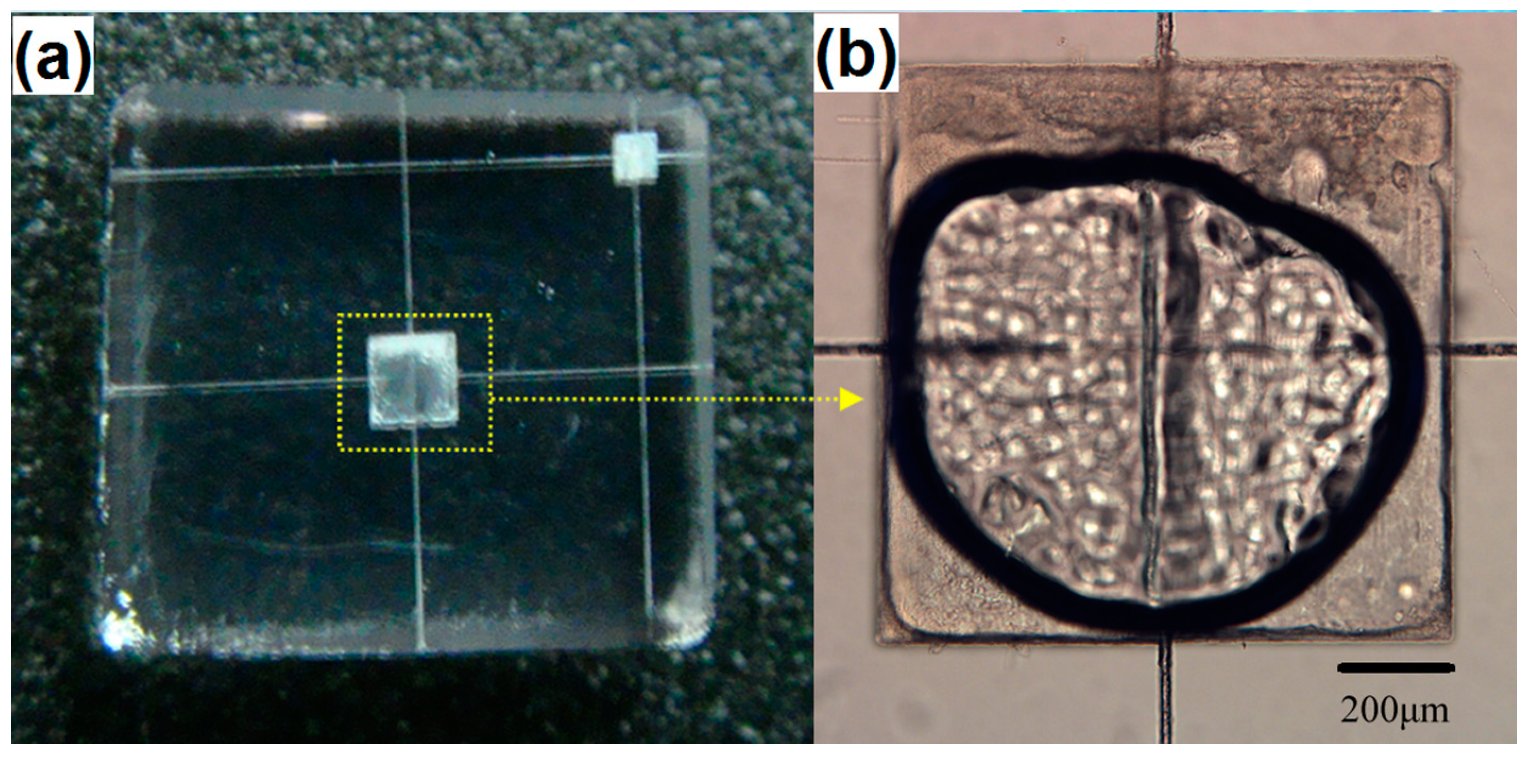
4.1. Large-Volume Hollow Chamber

Recently, 3D cell culture system has attracted wide attention of researchers range from engineering tissues for clinical delivery through to the development of models for drug screening, where both gene expression and other biological activities more closely mirror what happen in living organisms [55]. To build 3D microfluidic devices for cell culture, hollow microfluidic chamber with relatively large volume and arbitrary 3D configurations are desirable.
Figure 12 shows the fabrication process of a large-volume chamber inside glass by femtosecond laser direct wiriting. Two straight channels were first fabricated inside the porous sample for inflow of water and ejection of debris. Along with the straight channels, a chamber was fabricated by translating the sample in a line-by-line and layer-by-layer manner. The scan of the chamber started from its bottom in order to avoid the extra aberration created by the previously formed hollow layers. After the laser direct writing, a post-annealing process was applied to the sample for removing all the nanopores in the glass. After postannealing, geometric sizes of the annealed hollow chamber decrease to 85% of the original one, while its shapes remain unchanged (also see Table 1).
Figure 13a shows a large-volume chamber connected to four microchannels embedded in the porous glass. Here, the 250-kHz femtosecond laser pulses with a pulse energy of ~6.5 μJ were tightly focused by an objective lens (N.A. = 0.90). Firstly, the microchannels were fabricated with one slow scan at a translation speed of 20 μm/s. The diameter of the microchannels is approximately 20 μm. Secondly, the microchamber was fabricated in a line-by-line and layer-by-layer manner at a higher translation speed of 100 μm/s. The interval between the adjacent lines in the horizontal plane is 3 μm, and the vertical interval between the adjunct layers is 5μm. This size of the microchamber was 1 mm × 1 mm × 100 μm defined by the number of adjacent lines, and the total scanning process for fabricating the chamber took ~20 h because of its large volume. The thick black curve in Figure 13b shows the boundary of air and water in the chamber, providing a clear evidence of the hollow structure. The technique allows for fabrication of arbitrary 3D hollow structures embedded in glass.
Figure 12. Schematic illustration of the fabrication process for large-volume hollow chamber.
Micromachines 05 01106 g012
Figure 13. (a) Over view image of a 1 mm × 1 mm × 100 μm chamber connected to four microchannels. (b) Enlarged view of the large volume chamber.
Micromachines 05 01106 g013

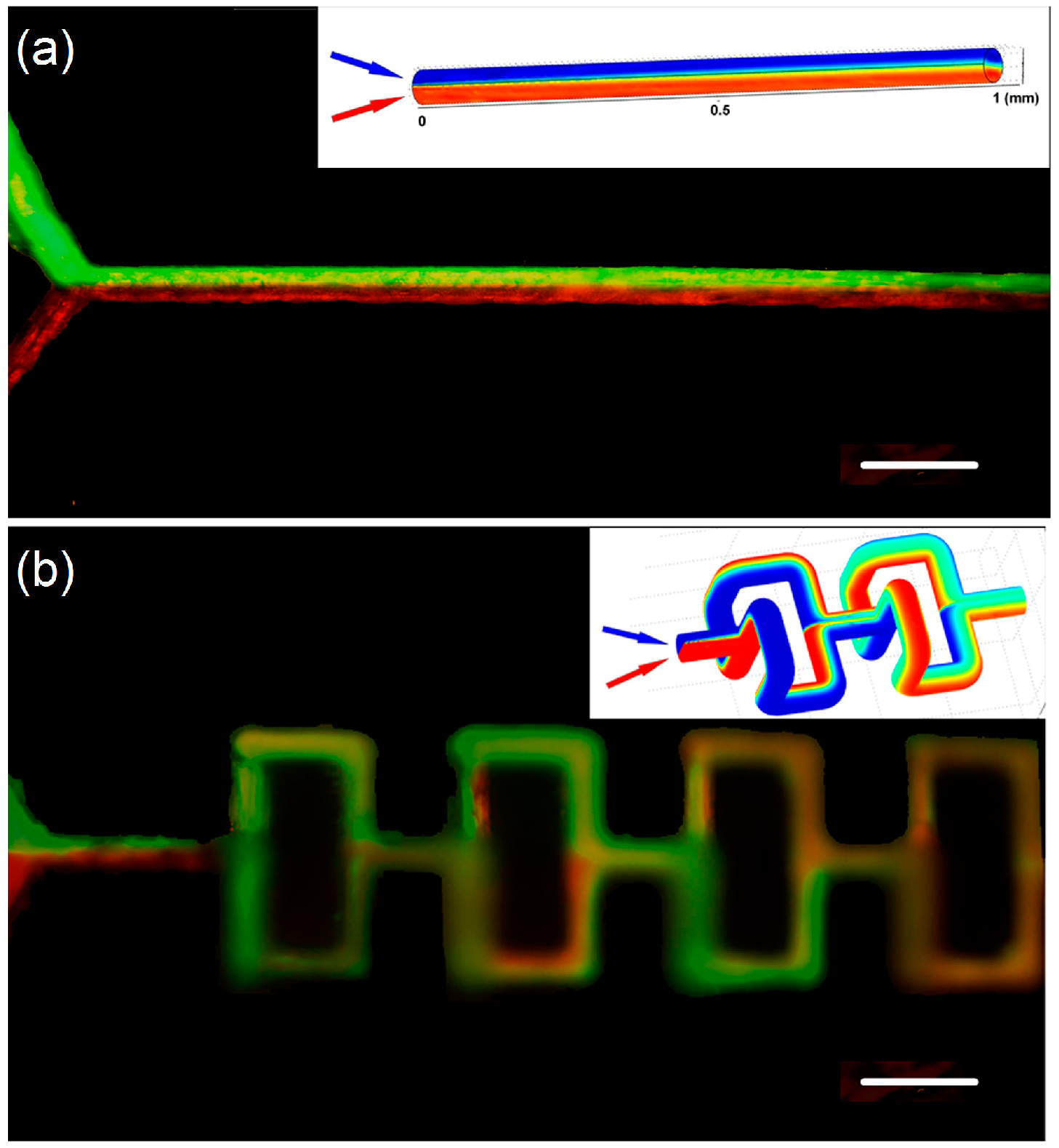
4.2. Three-Dimensional Microfluidic Mixer

Fluid mixing is an essential function required by most microfluidic systems. However, fast and efficient fluid mixing inside microchannels is usually difficult to achieve due to the laminar nature of microflows, characterized by low Reynolds numbers. Recently, various passive mixers have been developed to achieve efficient mixing by utilizing 3D geometric structures to induce disturbance in the fluids [56,57,58,59,60,61,62,63,64]. Nevertheless, the fabrication of 3D microfluidic mixer with arbitrary geometries is still challenging. Here, we demonstrate rapid fabrication of a passive microfluidic mixer consisting of geometrically complex 3D microchannels by femtosecond laser direct writing in porous glass.
According to the chaotic theories, a passive micromixer based on the baker’s transformation concept could provide ideal mixing performance [65]. However, such kinds of mixers usually require complicated 3D geometries, thus they are difficult to fabricate by the conventional planar fabrication process. By use of the femtosecond laser direct writing, we fabricated a passive micromixer consisting of symmetrical 3D units as theoretically proposed by Carrière [66]. Figure 14a,b presents the schematic illustrations of the designed 3D mixer which is composed of a Y-shape microchannel embedded 400 μm below the surface of chip and a string of mixing units, connected to two opening inlets and one outlet. The inlets and outlet are all on the backside of the chip. Three circular slots surrounding the inlets and the outlet were also fabricated by femtosecond laser ablation, which were used as connection interfaces with plastic pipes of a diameter of 0.9 mm. Figure 14c presents an overview of a 3D micromixer consisted of six mixing units. The length of all the horizontal and vertical channels in each mixing unit is 150 μm, as shown in Figure 14d (top view), e (side view). It also can be observed from Figure 14e that the cross section of channel is elliptical with a width of ~50 μm and a depth of ~75 μm. Figure 14f shows the inner surface of the microchannel for evaluation of the surface roughness.
Figure 14. Schematic diagrams of the 3D passive microfluidic mixer: (a) overview and (b) close-up view images. (c) Overview optical micrograph of the microfluidic mixer, (d) top view optical micrograph of two mixing units, and (e) cross sectional optical micrograph of the 3D microchannels. (f) Scanning electronic micrograph of the inner wall of the fabricated microchannel. The dark sections in (e) are caused by the bubbles [39] (Reproduced with permission from RSC. ©2012 by the Royal Society of Chemistry).
Micromachines 05 01106 g014
Figure 15a,b shows the experimental results of mixing of the two fluorescent dye solutions (fluorescein sodium and Rhodamine B) in the 1D and 3D microfluidic mixers fabricated under the same direct writing conditions, respectively. Clearly, the mixing behaviors in these two structures agree well with the simultion results. For the 3D mixer, after passing through three mixing units (i.e., a length of 0.9 mm), the two fluids are well mixed, corresponding to a mixing time of ~10 ms. For comparison, Figure 15a shows that in the 1D microfluidic channel, efficient mixing was not achieved after a propagation distance of ~1300 μm. The insets in Figure 15a,b shows the numerical simulations of mixing in 1D and 3D microfluidic mixers, respectively. It can be clearly seen that the experimental results and the computational results are in good agreement.
Figure 15. Fluorescence microscopy images of the (a) 1D and (b) 3D microfluidic mixing experiments, where two fluids (red and green) are mixed at Reynolds number (Re) = 5.3. Scale bars = 150 μm. Insets: Numerical simulations of mixing in (a) 1D and (b) 3D microfluidic mixers. Re = 5.3.
Micromachines 05 01106 g015

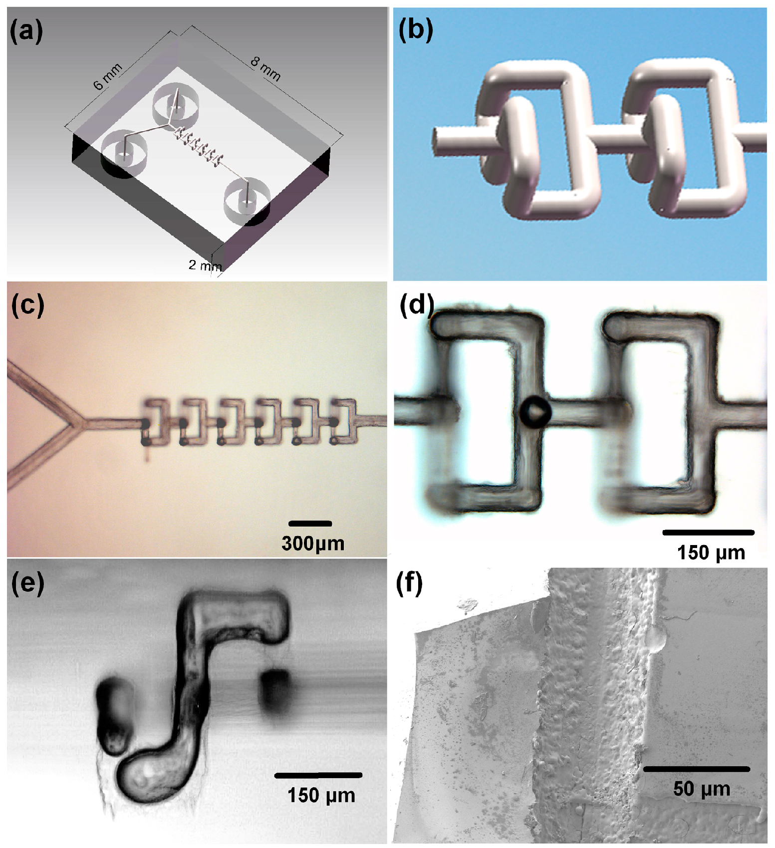
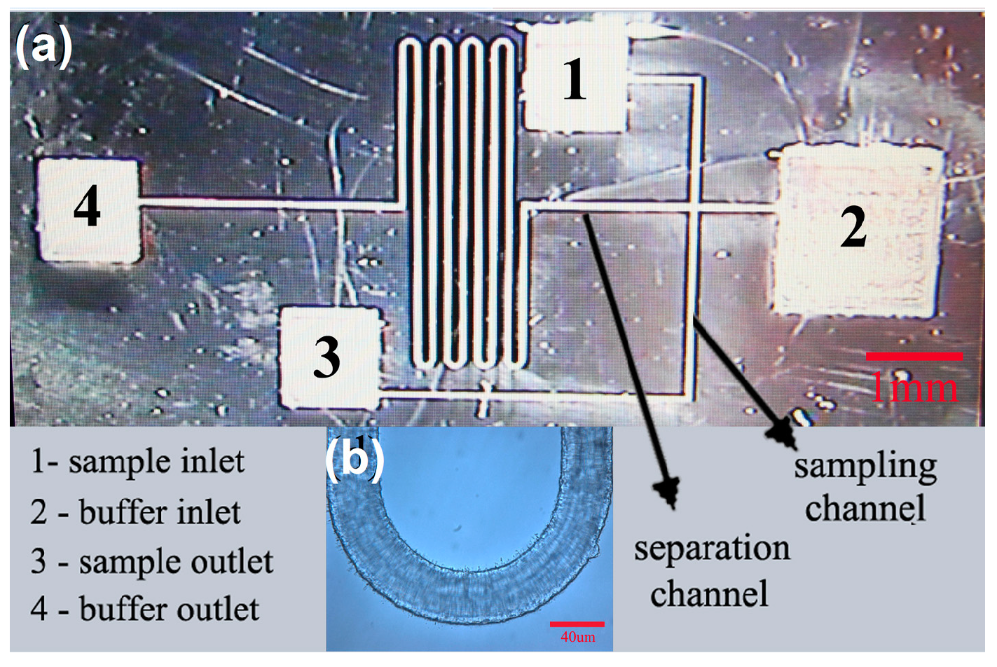
4.3. Electrophoresis Microchip

Electrophoresis is an important approach for performing chemical and biological analysis, which achieves separation of charged analytes with different size to charge ratios by accelerating them to different velocities in a conductive liquid in thin capillaries under the influence of an electric field. Nowadays, it is more and more popular to perform CE experiments in microfluidic channels fabricated on microchips, as the microfluidic CE chips typically consume only picoliters of samples and produce less waste [1]. Further development of microfluidic-chip CE technique requires integration of preparation and analysis functions into the microchips. Toward this goal, femtosecond laser 3D micromachining holds great promise as it has been demonstrated for creating a variety of functional components including microfluidics, microoptics, microelectrodes, etc. [67]. For example, integration of optical waveguides into a commercially produced CE device has been demonstrated by femtosecond laser direct writing, showing enhanced functionality and ease of operation [68]. Nevertheless, in this example, the CE device is prefabricated using traditional lithography technology, due to the difficulty in forming homogeneous large-scale microfluidic network embedded inside glass with traditional femtosecond laser micromachining techniques. In this Section, we show that the difficulty can be solved by direct writing with tightly focused femtosecond laser pulses in the porous glass. We demonstrate a fully functional capillary electrophoresis (CE) analysis chip and test its functionality by observing the motion of three amino acids, namely, l-Histidine, l-Lysine and dl-Alanine in the microfluidic channels.
The completed microchip is shown in Figure 16a, and a close-up view of the corner area of the microchannel is shown in Figure 16b. The smooth edge of the channel indicates that the ablation debris generated during the laser writing has been efficiently removed. The lengths of the microchannel connecting the buffer inlet and outlet and of that connecting the sample inlet and outlet are 35 mm and 8 mm, respectively, as shown in Figure 16a. In addition, the channels have a depth of ~10 μm and a width of ~36 μm. The channel width could be controlled by scanning the femtosecond laser line-by-line, as we have demonstrated before [38]. We tested the functionality of the CE device fabricated by femtosecond laser by observing the motion of three amino acids, namely, l-Histidine, l-Lysine and dl-Alanine in the microfluidic channels. After the derivatized amino acids were added into the inlet, a voltage of 200 V was applied across the sampling channel. The voltage applied across the migration channel was 100 V. After 2 s, the amino acids were driven into the junction of the two microchannels. With a migration voltage of 620 V applied across the migration channel and 200 V across the sampling channel, movement of the amino acids with a migration velocity of ~0.49 mm/s was observed under a fluorescence microscope.
Currently, most CE microchips used to separate analytes are fabricated on polymer/glass substrates based on lithography approaches. Polymer CE chips are easy to fabricate and the inner wall of the microchannel can be easily modified. However, the electro-osmotic flow can be unstable in polymer channels, which will decrease the separation efficiency. In addition, for CE chips fabricated using planar lithography techniques, sealing of the open channels fabricated on the upper substrate surfaces always poses a problem because complete sealing of tiny channels on the micrometer or even nanometer scales frequently causes clogging and/or leakage. We stress that these problems can be well addressed via our technique, as we have shown above.
Figure 16. (a) Overview optical micrograph of the fabricated electrophoresis microchip. (b) Close-up view of the turning area of the microchannel.
Micromachines 05 01106 g016

5. 3D Nanofluidic Channels and Devices

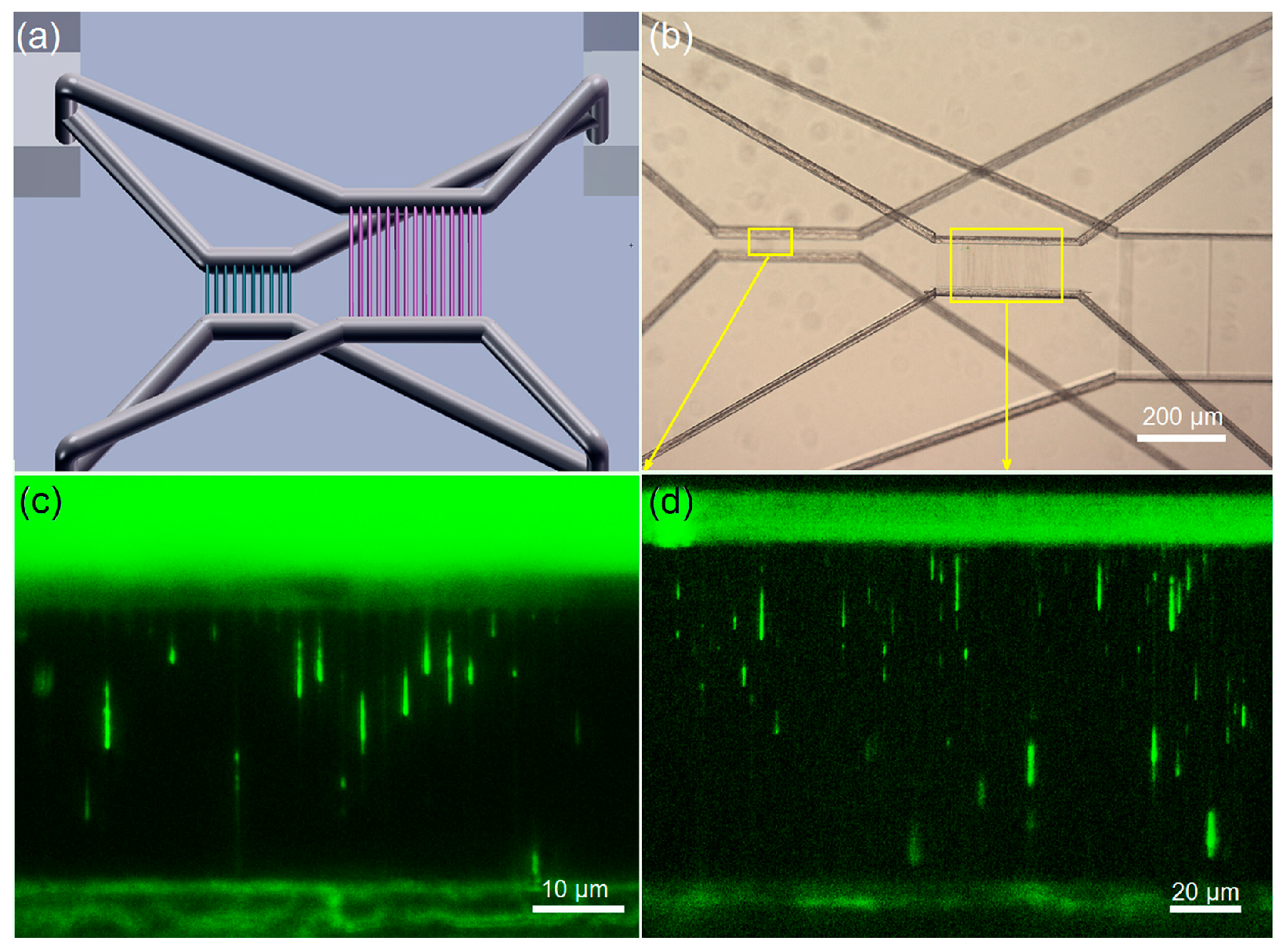
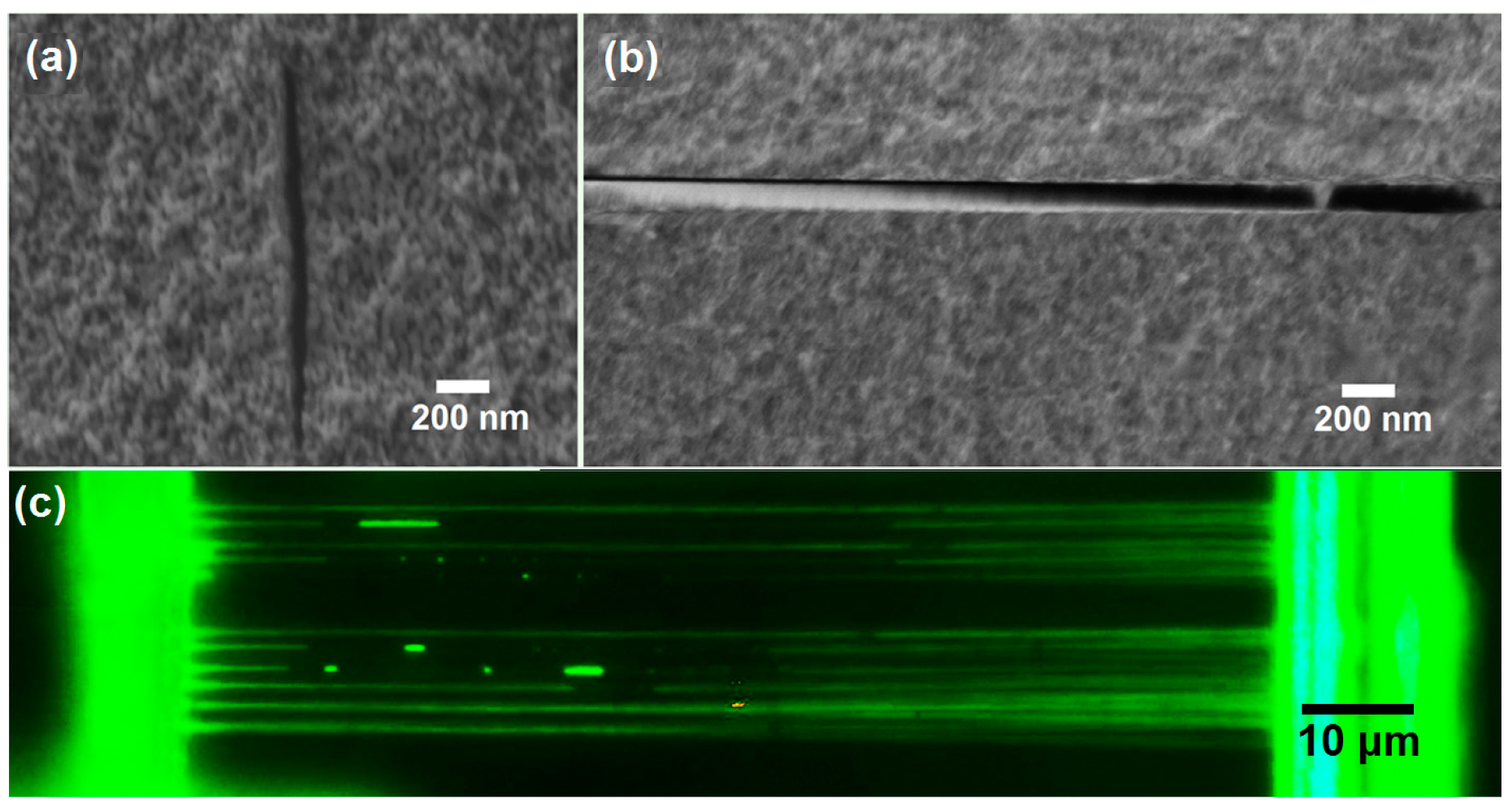
5.1. Direct Writing of Nanochannels

Recently, nanofluidics has attracted increasing attention due to its unique fluid transport properties and great potential to handle and probe individual biomolecules [69]. The incorporation of nanofluidic elements into microfluidic devices enables further downsizing of micro-analysis systems and enhancement of their functionalities, both of which are highly desired for lab-on-a-chip applications [70]. Both fundamental investigation and practical application of nanofluidics heavily rely on fast and simple nanofabrication techniques [71,72,73]. Here, we show that by uniquely employing the porous glass as the substrate material, nanogratings consisting of an array of elliptical-shaped hollow nano-voids elongated in the direction of laser propagation can be formed in glass using linearly polarized writing beam. By reducing the peak intensity of the laser pulses close to a threshold value, only a single hollow nano-void in the central area of the focal spot can survive, serving as the basic element for construction of 3D nanofluidics inside glass.
Previously, it has been reported that nanogratings can be formed in glass with femtosecond laser irradiation, which consist of alternating regions of high and low etch rates periodically distributed in a direction perpendicular to the laser polarization [74,75,76]. We found that the nanograting-like structures can also be induced in the porous glass by femtosecond laser irradiation, whereas the gratings are composed of an array of hollow nano-voids [37], as schematically shown in Figure 17.
Figure 17. Schematic diagram of inducing nanograting structures inside water-immersed porous glass by femtosecond laser pulses. The sample is translated in the x-y plane, the writing polarization is aligned to the x-axis, and the laser incident direction is along the z-axis [37] (Reproduced with permission from OSA. ©2013 by the Optical Society of America).
Micromachines 05 01106 g017
Amazingly, we found that a single nanochannel could still be induced in the central area of the focal volume at very low laser intensity, while other nanograting-like channels vanish. The cross sections of the nanogratings induced by femtosecond laser direct writing at different pulse energies (with a same writing speed of 10 μm/s) are shown in Figure 18a–c. The direction of laser polarization is perpendicular to the translating direction. At a relatively high pulse energy of 90 nJ, the number of the elliptical nano-voids in the grating is large, as shown in Figure 18a. By reducing the pulse energy to 70 nJ, the number of the nano-voids decreases to only four. It is noteworthy that under this condition, the periodicity of the nanograting apparently increases as evidenced in Figure 18b, which also helps reduce the number of nano-voids. Finally, by reducing the pulse energy to 60 nJ, only the central nano-void survives, showing an extremely narrow width of ~37 nm as presented in Figure 18c.
Figure 18d–f presents a principle schematic diagram to achieve a single nanocrack by combining the threshold effect and the formation of periodic nanograting. Conventionally, the surface nanostructuring of glass beyond the diffraction limit could be achieved by taking advantage of a threshold effect, i.e., by bringing the laser intensity down to a level approaching a threshold laser intensity only above which the ablation of glass induced by multiphoton absorption occurs [77,78]. In theory, there is no limit on the fabrication resolution when the threshold effect takes place, because the ablation linewidth can always be reduced if one keeps on reducing the difference between the chosen laser intensity and the threshold intensity. However, in practice, due to the fluctuation of the output power of the femtosecond laser, the fabrication process will become extremely unstable when the laser intensity is near the threshold intensity [79]. As a matter of fact, reliable sub-100 nm fabrication linewidth is extremely difficult to achieve for surface ablation. Moreover, sub-100 nm fabrication linewidth has never been demonstrated for 3D nanostructuring in bulk transparent materials so far due to the different physical mechanism involved in bulk machining [80]. In our case, the formation of a single nanocrack is much less sensitive to the fluctuation of the laser intensity by combining the threshold effect and the formation of a periodic nanograting. As shown in Figure 18f, when the femtosecond laser intensity is intentionally reduced to a level at which only the intensity in the blue region is higher than the threshold intensity, one will be able to select only one nanocrack in the central area of the focal volume. Note that the single nanocrack (green) is much narrower than the above-threshold-intensityregion (blue). So there exists a window (a range of laser intensity) for inducing a single nanocrack, which is between the threshold laser intensity of emergence of a single nanocrack and the minimum laser intensity for inducing two nanocracks in porous glass.
The induced single nano-voids can be connected into a continuous structure for construction of 3D nanochannels in glass. This is achieved by slowly scanning the focal spot of the femtosecond laser at a translation speed of 5–10 μm/s in the porous glass immersed in water. The nanochannel is connected to a prefabricated microchannel through which the debris can be driven out from the nanochannel by bubble generation. Figure 19a presents a zoom-in view of the cross section of the nanochannel surrounded by small nanopores. The top view image gives a direct evidence on the formation of a single continuous nanochannel, as shown in Figure 19b. After the laser writing, the sample was annealed at a high temperature of 1120 °C for 2 h. Figure 19c shows a fluorescence microscope image of the postannealed nanochannels filled with fluorescent dyes, indicating that there are no clogs and leakage in the nanochannels.
Figure 18. (ac) Evolution from nano-void array to single nano-void with decreasing laser intensity. The laser incident direction (k), polarization (E), and writing direction (S) are indicated [37] (Reproduced with permission from OSA. ©2013 by the Optical Society of America). (df) Principle schematic diagrams to achieve a single nanocrack [42] (Reproduced with permission from Springer. ©2014 by Springer).
Micromachines 05 01106 g018
Figure 19. (a) Cross section view and (b) top view SEM images of a continuous nanocrack written in the porous glass. (c) Fluorescence microscope image of the postannealed nanofluidic channels filled with fluorescent dyes as an evidence that these nanochannels are through structures without clogging and leakage [37] (Reproduced with permission from OSA. ©2013 by the Optical Society of America).
Micromachines 05 01106 g019

5.2. Rapid Prototyping of 3D Nanofluidic Chip

The unique 3D capability of femtosecond laser direct writing allows fabrication of nanochannels at arbitrary depths inside the glass substrate with a high axial resolution. Moreover, the dimensions of the channel can easily be controlled by adjusting the machining parameters, such as the laser pulse energy, the translation speed and the number of repeated scans. In combination with 3D microfluidics we have demonstrated in the previous sections, we now are capable of producing integrated micro-nanofluidic systems of complex 3D geometries and configurations in glass in a single continuous step.
Figure 20 shows a schematic diagram of the process flow chart for fabricating integrated 3D micro-nanofluidic structures by femtosecond laser direct writing in porous glass, showing four major steps: (1) fabrication of reservoirs by femtoseond laser direct write ablation of porous glass immersed in water with a low-NA objective (N.A.=0.45) at a pulse energy of ~10 μJ, as shown in Figure 20a; (2) direct writing of microchannels connecting the reservoirs with a long-working-distance water-immersed objective (N.A.= 1.10) at a pulse energy of 0.5–3 μJ, as shown in Figure 20b; (3) direct writing of a nanochannel array bridged between two microchannels with the same objective used in (2) but at a reduced pulse energy of 125–200 nJ, as shown in Figure 20c; and (4) postannealing of the glass substrate at ~1120 °C for 120 min, by which all the nanopores in porous glass can be collapsed to form a consolidated glass substrate, while the fabricated nanochannels could survive due to their larger diameter than the pores.
Figure 21a schematically illustrates an integrated micro-nanofluidic structure, which contains an array of two-layer nanochannels connected to two microfluidic channels. Figure 21b shows the optical micrograph of the fabricated nanochannel arrays. The nanochannels were directly written at the depths of about 200 μm below the porous glass surface, and the difference in the depths of the two layers of the nanochannels is only ~1.5 μm. All the nanochannels were directly written by a single scan at a translating speed of 10 μm/s with a pulse energy of 128 nJ. Note that as we have examined prior to the writing process, the threshold pulse energy for inducing optical breakdown in porous glass immersed in water is ~108 nJ. Therefore, the peak laser intensity we chose for writing the nanochannel is approximately ~20% higher than the threshold intensity. The direction of laser polarization was perpendicular to the translating direction. During the fabrication of the nanochannel in porous glass immersed in water, it could be observed that the bubbles were continuously ejected from the inlet of the fabricated nanochannel into the thick microchannel, which can efficiently remove the debris produced by laser ablation. The continuous bubble flow in turn indicates that an unclogged nanochannel has been formed with a single scan (we observed previously that once clogging occurred, there would be no more bubbles coming out from the outlet.). After collapsing the nanopores by the postannealing, the size of each nanochannel was reduced by ~14% isotropically in all three dimensions, resulting a total channel length of ~40 μm, a width in the range of 30–50 nm, and a height in the range of 1–1.5 μm, as shown in Figure 21b,c. The cross section of the nanochannel appears highly elliptical, showing a typical depth-to-width ratio up to 25, as evidenced in Figure 21d. Such highly elliptical shape resembles the cross section of an individual nanoplane in a nanograting, indicating a relatively low fabrication resolution in the axial resolution.
Figure 20. Schematic diagram of process flow chart for fabricating 3D integrated micro-nanochannels by femtosecond laser direct writing.
Micromachines 05 01106 g020
Figure 21. (a) Schematic diagram of an array of double-layer nanochannels to bridge two microchannels. (b) Top-view optical micrograph of double-layer nanochannels after postannealing. (c) Cross-sectional SEM micrograph of the nanochannels cleaved along the red dashed line in (b). The laser was incident from bottom of the figure, and the blue arrows indicate some tiny occasional protrusions on the edges of the nanochannels, which were formed due to the cleaving process. (d) Close-up SEM micrograph of cross section of a nanochannel [41] (Reproduced with permission from RSC. ©2013 by the Royal Society of Chemistry).
Micromachines 05 01106 g021
To demonstrate the applications of the fabricated nanochannels in investigating single molecular behaviors, we fabricate a complex 3D micro-nanofluidic device as illustrated in Figure 22a and perform an experiment of DNA stretching using the fabricated device. It is noteworthy that recently, nanochannel-based DNA stretching has attracted enormous attention because of its potential use in DNA analysis, whereas until now direct fabricating nanochannels and realizing 3D micro- and nanofluidic integration within bulk glass have not yet been achieved [81]. The device consists of two nanochannel arrays with different dimensions (i.e., widths and lengths) at different depths embedded in a single glass substrate. The nanochannels are connected to the four common reservoirs through two microchannels with a diameter of ~50 μm. Such a device allows for simultaneously observing the stretching of DNA molecules in the two nanochannel arrays of different dimensions.
Figure 22b presents a top view of the fabricated two nanochannel arrays, in which the short nanochannels have a length of ~30 μm and a cross section of ~50 nm × 1 μm, whereas the long nanochannles have a length of ~100 μm and a cross section of ~200 nm × 1.2 μm. After an aqueous buffer solution of stained λ DNA was pipetted into a reservoir, the DNA molecules can readily transported into the nanochannels by capillary force. Figure 22c,d is typical image of stretching of λ DNA in the nanochannels. In the thin nanochannels with a cross section of 50 nm × 1 μm, the average stretched length of DNA is ~6.4 ± 1.0 μm (~30% of the dye-adjusted contour length). In the thicker nanochannels with a cross section of ~200 nm × 1.2 μm, the average stretched length of DNA is ~2.8 ± 0.6 μm (~13% of the dye-adjusted contour length). The apparent lengths of some stretched DNA molecules in Figure 22d can reach as long as ~15 µm, which can be attributed to the clustering of the DNA molecules. As shown in these images, the continuous flow and uniform stretching of the DNA molecules in the nanochannel arrays also verify the continuity of the nanochannels and the repeatability of the direct writing process.
Figure 22. (a) Schematic diagram and (b) top-view optical micrograph of the fabricated 3D nanofluidic device for DNA analysis; and fluorescent images showing the stretching of λ DNA in two arrays of nanochannels with different widths: (c) 50 nm and (d) 200 nm [41] (Reproduced with permission from RSC. ©2013 by the Royal Society of Chemistry).
Micromachines 05 01106 g022

6. Mechanism Investigation

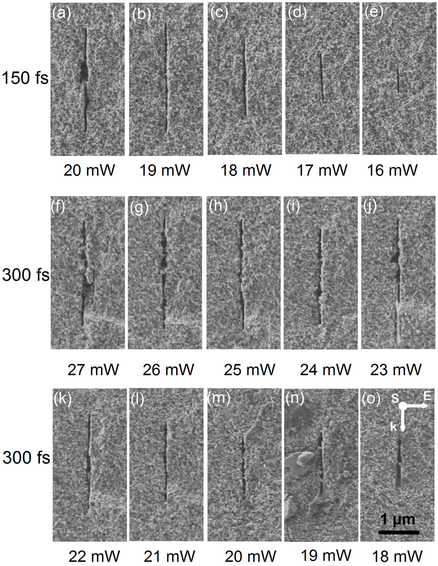
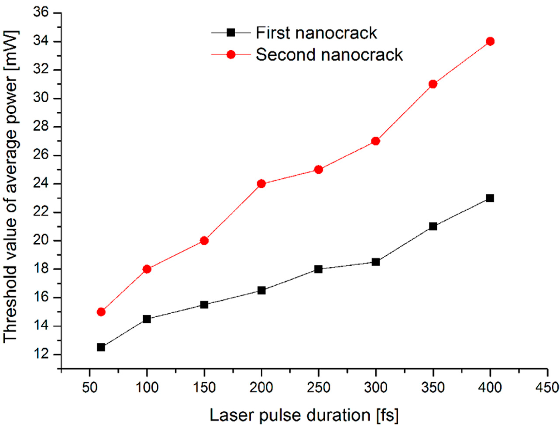
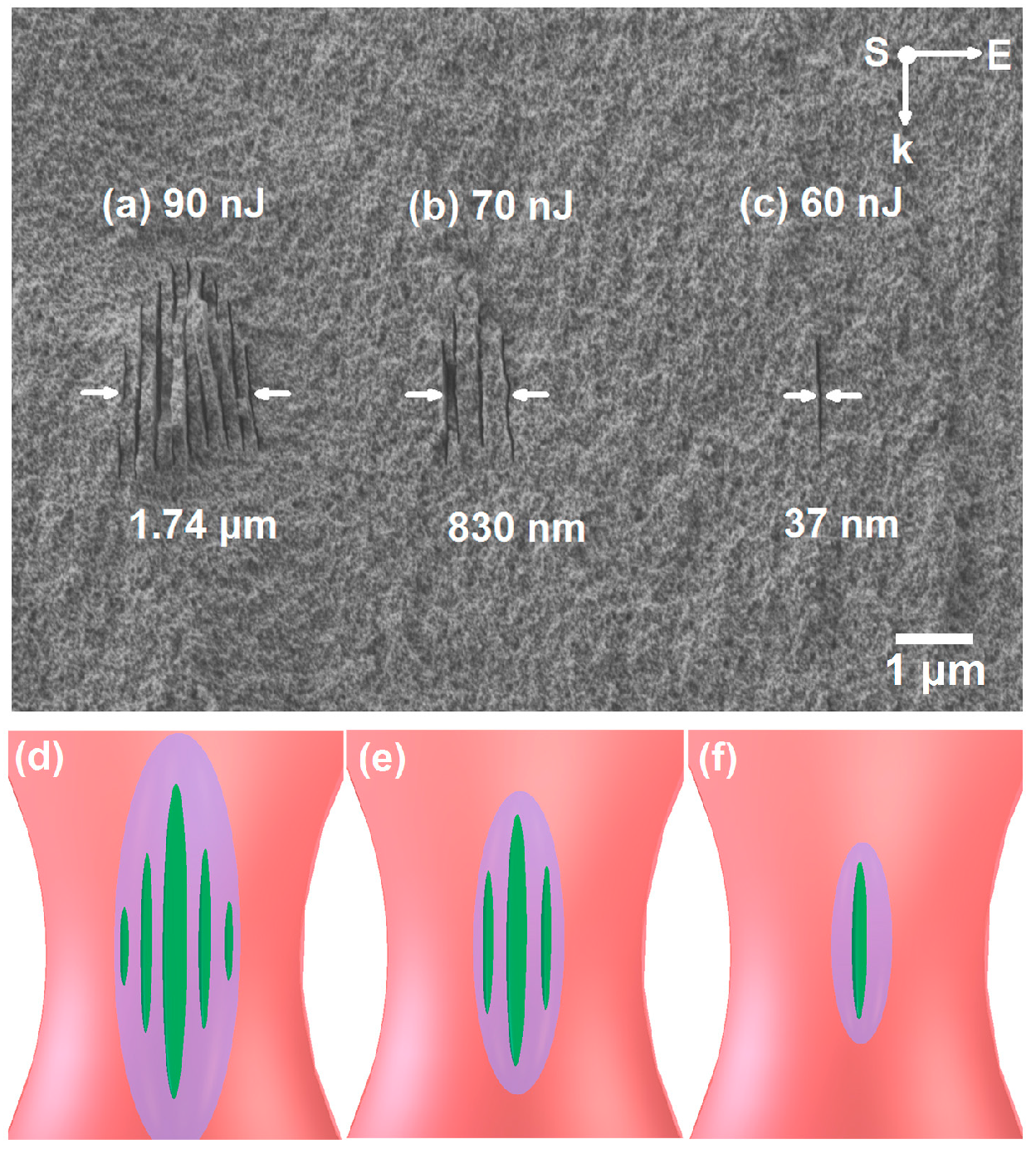
6.1. Pulse Duration Dependence

In previous section, we proposed that the mechanism behind the formation of a single nanochannel can be understood as a combination of the threshold effect and the formation of periodic nanograting during the process of laser writing in a porous glass immersed in water. Compared with traditional nanostructuring technique only utilizing threshold effect, the new-established nanostructuring strategy is relatively not sensitive to the laser peak intensity, and there exists a window (a range of laser intensity) for inducing a single nanochannel. Here, we show that the effective range of laser intensity for fabrication of nanochannel can be expanded by optimizing the laser pulse duration [42].
Figure 23 shows morphological changes of a single nanocrack induced by different laser powers and pulse durations. For the first row, the nanograting structures were written with ~150 fs pulses, whereas for the second and third row, the nanograting structures were written with ~300 fs pulses. One can see that when the laser intensity increases, the longitudinal length (i.e., the height) of the nanochannel increases, too, which is a manifestation of the threshold effect. The most significant information conveyed from these images is that at the ~300 fs pulse duration, the effective range of laser intensity for creating a single nanocrack has a broad range from ~18 mW to ~26 mW, as shown in Figure 3f–o. In contrast, at the relatively shorter pulse duration of ~150 fs, the effective range of laser intensity for creating a single nanocrack shrinks to a smaller range from ~16 mW to ~19 mW, as shown in Figure 23a–e. In other word, in the case of nanograting fabrication with the ~300 fs pulses, the laser intensity can be varied by nearly ~45% (i.e., (26−18)/18) while a single nanocrack structure can still be maintained. However, for the case of nanograting fabrication with the ~150 fs pulses, the variation of laser intensity has to be limited to ~20% for avoiding the formation of double nanocracks.
Figure 23. SEM images of double and single nanocrack inside porous glass induced by different laser powers and pulse durations. (ae) 150 fs; (fo) 300 fs [42] (Reproduced with permission from Springer. ©2014 by Springer).
Micromachines 05 01106 g023
Figure 24 presents the pulse duration dependence of the threshold power for formation of a single nanocrack and double nanocracks. The range of laser intensity for producing only a single nanocrack in nanograting formation can be broadened by elongation of the laser pulse duration. However, when the pulse durations are longer than ~300 fs, the roughness of sidewalls in the nanocracks becomes high probably due to the more severe heat effect. When the femtosecond laser pulses of a duration of ~200 fs are chosen, a sufficiently broad range of laser intensity (~44% of the structuring threshold) for creating a single nanocrack can be achieved, while smooth sidewalls required by nanofluidics applications can still be maintained. The broadened processing window can make the fabrication more stable against the fluctuation of laser peak intensity and the fabricated nanofluidic structures more uniform. In addition, the dependence of the effective range of laser intensity for fabrication of nanochannel, which relies on the formation of a single nanocrack in a nanograting, will shed more light on the mechanism behind the nanograting formation in transparent materials with femtosecond laser irradiation.
Figure 24. The laser threshold power for formation of a single nanocrack and double nanocracks as functions of femtosecond laser pulse duration [42] (Reproduced with permission from Springer. ©2014 by Springer).
Micromachines 05 01106 g024

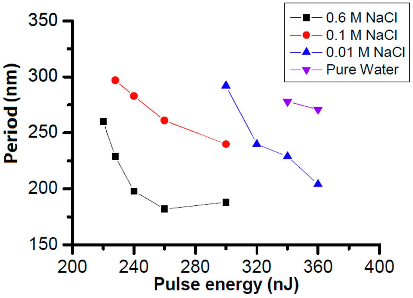
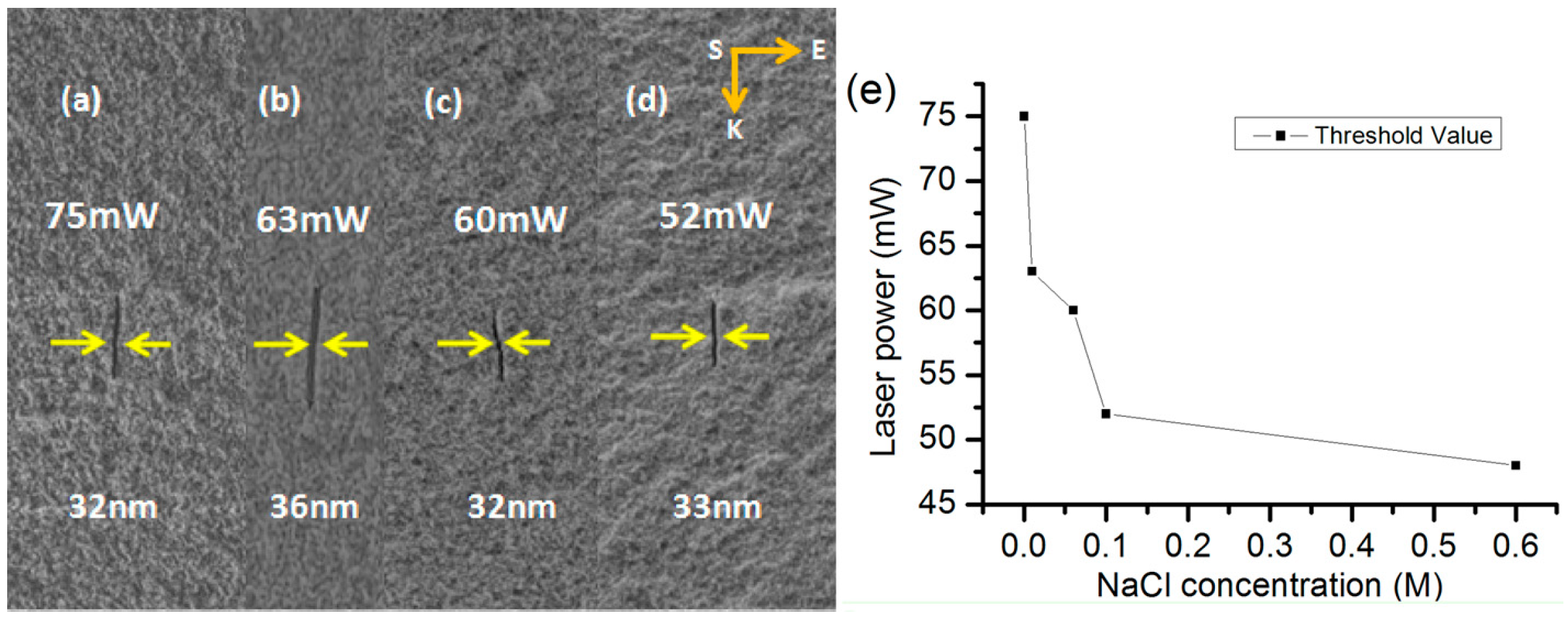
6.2. Influence of Ionization Property of Immersion Liquid

Over the recent decade, formation of nanogratings inside transparent materials by femtosecond laser irradiation has attracted broad attention because of its sub-diffraction-limit nature and its potential for optical, polarization sensitive and fluidic applications [82,83]. However, although great effort has been made on investigating the mechanism behind this phenomenon, a clear picture is still lacking until now [75,84]. Recently, it has been found that nanogratings can also be formed in a porous glass immersed in water by irradiation with femtosecond laser pulses of carefully selected pulse energies [37]. For the mechanism exploration, such porous material also provides unique opportunities to continuously tune the material properties by filling different types of solutions into the nanopores. For example, optical properties could be tuned by filling liquids with different nonlinear optical coefficients. Here, we place our focus on tuning the ionization property of the porous glass by doping the immersion water with NaCl at different concentrations [43].
Figure 25a–d shows the SEM images of a series of single nanocracks formed inside the porous glass immersed in water doped with NaCl at different concentrations. It can be concluded that the threshold power for inducing optical breakdown in the porous glass immersed in NaCl solution decreases with increasing of the concentration of NaCl, while the width of a single nanocrack almost does not change. The same trend can also be seen in Figure 2e, in which the dependence of the threshold fluence of single-crack formation on the concentration of NaCl is plotted.
Figure 26 quantitatively shows how the period of nanograting evolves with the increasing laser power and increasing concentration of NaCl in water. Generally speaking, at a fixed concentration of NaCl, the period of nanogratings decreases with increasing power, which is consistent with the results reported previously [85,86]. On the other hand, we find that at a fixed output power of femtosecond laser, the period of nanogratings decreases with increasing concentration of NaCl in water. The comparison of these observations seems to suggest that a stronger ionization, which could be realized either by increasing the laser peak intensity or by reducing the ionization threshold, would lead to smaller period of the nanograting structures. This is consistent with the previous observation [87]. In our opinion, the decreasing period with enhancement of photoionization may suggest that an above critical density has been reached, resulting in a semiopaque plasma.
These results we obtained not only suggest a practical way for promoting the fabrication efficiency due to the reduction of the ablation threshold in water by doping of NaCl, but also could shed new light on the mechanism behind the nanograting formation. Firstly, due to the fact that tuning of ionization threshold is achieved by changing the concentration of NaCl in water, as a result, it is the free electrons generated from the liquid that induce the subsequent ionization and ablation in the porous glass. Secondly, we may conclude that the formation of nanograting heavily depends on the density of electrons in the excitation region, as higher electron density could be achieved with either higher peak intensity or lower ionization potential, which in turn causes formation of the gratings of smaller period.
Figure 25. Nanogratings formed in porous glass by induced by femtosecond laser pulses at threshold fluencies in different immersion liquids: (a) water, (b) 0.01 M of NaCl solution, (c) 0.06 M of NaCl solution, and (d) 0.1M of the same solution. (e) Dependence of the threshold fluence of single-crack formation on the concentration of NaCl [43] (Reproduced with permission from OSA. ©2013 by the Optical Society of America).
Micromachines 05 01106 g025
Figure 26. The dependence of nanograting period on laser power at different doping concentrations of NaCl [43] (Reproduced with permission from OSA. ©2013 by the Optical Society of America).
Micromachines 05 01106 g026

7. Conclusions and Future Outlook

In this review, we have shown that fabrication of 3D homogeneous microchannels with large sizes and complex geometries can be achieved using water-assisted femtosecond laser direct writing in porous glass followed by a postannelaing for consolidation of the porous glass. By further manipulating the laser pulse energy and polarization, nanofluidic channels with a width of ~30 nm, which is less than λ/25 (here λ = 800 nm, which is the wavelength of the writing beam), and an aspect ratio above ~1000 can be directly written in the porous glass, enabling straightforward integration of microfluidics and nanofluidics in a single platform. Interestingly, two extreme nonlinear effects, namely, the femtosecond-laser-induced nanograting formation and the threshold effect in femtosecond laser induced optical breakdown in glass, play important roles in fabrication of the nanochannels. Based on this technique, several functional devices built in glass that cannot be produced by any previous laser direct writing techniques, including a 3D passive microfluidic mixer, an integrated DNA analysis chip, etc., have been demonstrated. This technique will open a broad spectrum of opportunities for micro- and nanofluidic applications.
Currently, however, this emerging field is still in its infancy from both fundamental and applied points of views. First of all, the underlying physical mechanisms behind the formation of nanogratings as well as water-assisted femtosecond laser direct writing in porous glass are quite complicated and not yet fully understood. Secondly, the roughness of microfluidic structures fabricated by laser direct writing needs to be further improved for in vivo and optofluidic applications. Thirdly, the fabrication efficiencies for large-volume and high-aspect-ratio microfluidic devices are still quite low. At last, the cross section of the nanochannel appears highly elliptical and asymmetrical, indicating a relatively low fabrication resolution in the axial resolution. We expect that the future advance in 3D micro-/nano-fluidic applied research will strongly promote the further development and optimization of the technique.

Acknowledgments

This research is financially supported by National Natural Science Foundation of China (Nos. 11127901, 61275205, 61108015, 61221064 and 11104294). The authors would like to thank Dr. Ling Ling Qiao for assisting with preparation of the manuscript.

Author Contributions

Yang Liao has written the main manuscript, and Ya Cheng provided guidance and revised the manuscript.

Conflicts of Interest

The authors declare no conflict of interest.

References

  1. Manz, A.; Graber, N.; Widmer, H.M. Miniaturized total chemical analysis systems: A novel concept for chemical sensing. Sens. Actuators B 1990, 1, 244–248. [Google Scholar]
  2. Whitesides, G.M. The origins and the future of microfluidics. Nature 2006, 442, 368–373. [Google Scholar]
  3. Bellouard, Y.; Champion, A.; Lenssen, B.; Matteucci, M.; Schaap, A.; Beresna, M.; Corbari, C.; Gecevičius, M.; Kazansky, P.; Chappuis, O.; Kral, M.; Clavel, R.; Barrot, F.; Breguet, J.-M.; Mabillard, Y.; Bottinelli, S.; Hopper, M.; Hoenninger, C.; Mottay, E.; Lopez, J. The femtoprint project. J. Laser Micro/Nanoeng. 2012, 7, 1–10. [Google Scholar] [CrossRef]
  4. Xiong, W.; Zhou, Y.S.; He, X.N.; Gao, Y.; Samani, M.M.; Jiang, L.; Baldacchini, T.; Lu, Y.F. Simultaneous additive and subtractive three-dimensional micro/nano-fabrication using integrated two-photon polymerization and multi-photon ablation. Light Sci. Appl. 2012, 1, e6. [Google Scholar] [CrossRef]
  5. Davis, K.M.; Miura, K.; Sugimoto, N.; Hirao, K. Writing waveguides in glass with a femtosecond laser. Opt. Lett. 1996, 21, 1729–1731. [Google Scholar] [CrossRef]
  6. Ams, M.; Dekker, P.; Marshall, G.D.; Withford, M.J. Monolithic 100 mW Yb waveguide laser fabricated using the femtosecond-laser direct-write technique. Opt. Lett. 2009, 34, 247–249. [Google Scholar] [CrossRef]
  7. Chen, F.; Vazquez de Aldana, J.R. Optical waveguides in crystalline dielectric materials produced by femtosecond- laser micromachining. Laser Photon. Rev. 2014, 8, 251–275. [Google Scholar] [CrossRef]
  8. Marcinkevicius, A.; Juodkazis, S.; Watanabe, M.; Miwa, M.; Matsuo, S.; Misawa, H.; Nishii, J. Femtosecond laser-assisted three-dimensional microfabrication in silica. Opt. Lett. 2001, 26, 277–279. [Google Scholar] [CrossRef]
  9. Masuda, M.; Sugioka, K.; Cheng, Y.; Aoki, N.; Kawachi, M.; Shihoyama, K.; Toyoda, K.; Helvajian, H.; Midorikawa, K. 3-D microstructuring inside photosensitive glass by femtosecond laser excitation. Appl. Phys. A 2003, 76, 857–860. [Google Scholar] [CrossRef]
  10. Matsuo, S.; Kiyama, S.; Shichijo, Y.; Tomita, T.; Hashimoto, S.; Hosokawa, Y.; Masuhara, H. Laser microfabrication and rotation of ship-in-a-bottle optical rotators. Appl. Phys. Lett. 2008, 93, 051107. [Google Scholar] [CrossRef]
  11. Masuda, M.; Sugioka, K.; Cheng, Y.; Hongo, T.; Shihoyama, K.; Takai, H.; Miyaloto, I.; Midorikawa, K. Direct fabrication of freely movable microplate inside photosensitive glass by femtosecond laser for lab-on-chip application. Appl. Phys. A 2004, 78, 1029–1032. [Google Scholar] [CrossRef]
  12. Cheng, Y.; Sugioka, K.; Midorikawa, K.; Masuda, M.; Toyoda, K.; Kawachi, M.; Shihoyama, K. Three-dimensional micro-optical components embedded in photosensitive glass by a femtosecond laser. Opt. Lett. 2003, 28, 1144–1146. [Google Scholar] [CrossRef]
  13. Cheng, Y.; Tsai, H.L.; Sugioka, K.; Midorikawa, K. Fabrication of 3D microoptical lenses in photosensitive glass using femtosecond laser micromachining. Appl. Phys. A 2006, 85, 11–14. [Google Scholar] [CrossRef]
  14. Wang, Z.; Sugioka, K.; Midorikawa, K. Fabrication of integrated microchip for optical sensing by femtosecond laser direct writing of Foturan glass. Appl. Phys. A 2007, 89, 951–955. [Google Scholar] [CrossRef]
  15. Cheng, Y.; Sugioka, K.; Midorikawa, K. Microfluidic laser embedded in glass by three-dimensional femtosecond laser microprocessing. Opt. Lett. 2004, 29, 2007–2009. [Google Scholar] [CrossRef]
  16. Hanada, Y.; Sugioka, K.; Kawano, H.; Ishikawa, I.S.; Miyawaki, A.; Midorikawa, K. Nano-aquarium for dynamic observation of living cells fabricated by femtosecond laser direct writing of photostructurable glass. Biomed. Microdevices 2008, 10, 403–410. [Google Scholar] [CrossRef]
  17. Hanada, Y.; Sugioka, K.; Ishikawa, I.S.; Kawano, H.; Miyawaki, A.; Midorikawa, K. 3D microfluidic chips with integrated functional microelements fabricated by a femtosecond laser for studying the gliding mechanism of cyanobacteria. Lab Chip 2011, 11, 2109–2115. [Google Scholar] [CrossRef]
  18. Crespi, A.; Gu, Y.; Ngamsom, B.; Hoekstra, H.J.W.M.; Dongre, C.; Pollnau, M.; Ramponi, R.; van den Vlekkert, H.H.; Watts, P.; Cerullo, G.; Osellame, R. Three-dimensional Mach-Zehnder interferometer in a microfluidic chip for spatially-resolved label-free detection. Lab. Chip 2010, 10, 1167–1173. [Google Scholar] [CrossRef]
  19. Kim, M.; Hwang, D.J.; Jeon, H.; Hiromatsu, K.; Grigoropoulos, C.P. Single cell detection using a glass-based optofluidic device fabricated by femtosecond laser pulses. Lab. Chip 2009, 9, 311–318. [Google Scholar] [CrossRef]
  20. Bragheri, F.; Ferrara, L.; Bellini, N.; Vishnubhatla, K.C.; Minzionil, P.; Ramponi, R.; Osellame, R.; Cristiani, I. Optofluidic chip for single cell trapping and stretching fabricated by a femtosecond laser. J. Biophoton. 2010, 3, 234–243. [Google Scholar] [CrossRef]
  21. Schaap, A.; Bellouard, Y.; Rohrlack, T. Optofluidic lab-on-a-chip for rapid algae population screening. Biomed. Opt. Express 2011, 2, 658–664. [Google Scholar] [CrossRef]
  22. Xu, J.; Liao, Y.; Zeng, H.D.; Sun, H.Y.; Song, J.; Wang, X.S.; Cheng, Y.; Xu, Z.Z.; Sugioka, K.; Midorikawa, K. Selective metallization on insulator surfaces with femtosecond laser pulses. Opt. Express 2007, 15, 12743–12748. [Google Scholar] [CrossRef]
  23. Liao, Y.; Xu, J.; Sun, H.Y.; Song, J.; Wang, X.S.; Cheng, Y. Fabrication of microelectrodes deeply embedded in LiNbO3 using a femtosecond laser. Appl. Surf. Sci. 2008, 254, 7018–7021. [Google Scholar] [CrossRef]
  24. Liao, Y.; Xu, J.; Cheng, Y.; Zhou, Z.H.; He, F.; Sun, H.Y.; Song, J.; Wang, X.S.; Xu, Z.Z.; Sugioka, K.; Midorikawa, K. Electro-optic integration of embedded electrodes and waveguides in LiNbO3 using a femtosecond laser. Opt. Lett. 2008, 33, 2281–2283. [Google Scholar] [CrossRef]
  25. Xu, J.; Wu, D.; Hanada, Y.; Chen, C.; Wu, S.Z.; Cheng, Y.; Sugioka, K.; Midorikawa, K. Electrofluidics fabricated by space-selective metallization in glass microfluidic structures using femtosecond laser direct writing. Lab Chip 2013, 13, 4608–4616. [Google Scholar] [CrossRef]
  26. Liao, Y.; Qiao, L.; Wang, Z.; Wang, M.; Liu, L.; Sugioka, K.; Cheng, Y. Fabrication of a liquid crystal light modulator by use of femtosecond-laser-induced nanoripples. Opt. Mater. Express 2013, 3, 1698–1704. [Google Scholar] [CrossRef]
  27. Bellouard, Y.; Said, A.; Bado, P. Integrating optics and micro-mechanics in a single substrate: A step toward monolithic integration in fused silica. Opt. Express 2005, 13, 6635–6644. [Google Scholar] [CrossRef]
  28. Lenssen, B.; Bellouard, Y. Optically transparent glass micro-actuator fabricated by femtosecond laser exposure and chemical etching. Appl. Phys. Lett. 2012, 101, 103503. [Google Scholar]
  29. Hnatovsky, C.; Taylor, R.S.; Simova, E.; Rajeev, P.P.; Rayner, D.M.; Bhardwaj, V.R.; Corkum, P.B. Fabrication of microchannels in glass using focused femtosecond laser radiation and selective chemical etching. Appl. Phys. A 2006, 84, 47–61. [Google Scholar] [CrossRef]
  30. Sugioka, K.; Cheng, Y.; Midorikawa, K. Three-dimensional micromachining of glass using femtosecond laser for lab-on-a-chip device manufacture. Appl. Phys. A 2005, 81, 1–10. [Google Scholar] [CrossRef]
  31. Sugioka, K.; Hanada, Y.; Midorikawa, K. Three-dimensional femtosecond laser micromachining of photosensitive glass for biomicrochips. Laser Photonics Rev. 2010, 4, 386–400. [Google Scholar] [CrossRef]
  32. Li, Y.; Itoh, K.; Watanabe, W.; Yamada, K.; Kuroda, D.; Nishii, J.; Jiang, Y.Y. Three-dimensional hole drilling of silica glass from the rear surface with femtosecond laser pulses. Opt. Lett. 2001, 26, 1912–1914. [Google Scholar] [CrossRef]
  33. Maruo, S.; Fourkas, J.T. Recent progress in multiphoton microfabrication. Laser Photon. Rev. 2008, 2, 100–111. [Google Scholar] [CrossRef]
  34. Ke, K.; Hasselbrink, E.F.; Hunt, A.J. Rapidly prototyped three-dimensional nanofluidic channel networks in glass substrates. Anal. Chem. 2005, 77, 5083–5088. [Google Scholar] [CrossRef]
  35. Liao, Y.; Ju, Y.; Zhang, L.; He, F.; Zhang, Q.; Shen, Y.; Chen, D.; Cheng, Y.; Xu, Z.; Sugioka, K.; Midorikawa, K. Three-dimensional microfluidic channel with arbitrary length and configuration fabricated inside glass by femtosecond laser direct writing. Opt. Lett. 2010, 35, 3225–3227. [Google Scholar] [CrossRef]
  36. Liu, C.N.; Liao, Y.; He, F.; Lin, D.; Song, J.X.; Lin, J.T.; Cheng, Y.; Sugioka, K.; Midorikawa, K. Compact 3D microfluidic channel structures embedded in glass fabricated by femtosecond laser direct writing. J. Laser Micro/Nanoeng. 2013, 8, 170–174. [Google Scholar] [CrossRef]
  37. Liao, Y.; Shen, Y.L.; Qiao, L.L.; Chen, D.P.; Cheng, Y.; Sugioka, K.; Midorikawa, K. Femtosecond laser nanostructuring in porous glass with sub-50nm feature sizes. Opt. Lett. 2013, 38, 187–189. [Google Scholar] [CrossRef]
  38. Ju, Y.; Liao, Y.; Zhang, L.; Zhang, Q.; Shen, Y.; Chen, D.; Cheng, Y.; Xu, Z.; Sugioka, K.; Midorikawa, K. Fabrication of large-volume microfluidic chamber embedded in glass using three-dimensional femtosecond laser micromachining. Microfluid. Nanofluid. 2011, 11, 111–117. [Google Scholar] [CrossRef]
  39. Liao, Y.; Song, J.; Li, E.; Luo, Y.; Shen, Y.; Chen, D.; Cheng, Y.; Xu, Z.; Sugioka, K.; Midorikawa, K. Rapid prototyping of three-dimensional microfluidic mixers in glass by femtosecond laser direct writing. Lab Chip 2012, 12, 746–749. [Google Scholar] [CrossRef]
  40. Ju, Y.; Liu, C.; Liao, Y.; Liu, Y.; Zhang, L.; Shen, Y.; Chen, D.; Cheng, Y. Direct fabrication of a microfluidic chip for electrophoresis analysis by water-assisted femtosecond laser writing in porous glass. Chin. Opt. Lett. 2013, 11, 072201. [Google Scholar] [CrossRef]
  41. Liao, Y.; Cheng, Y.; Liu, C.N.; Song, J.X.; He, F.; Shen, Y.L.; Chen, D.P.; Xu, Z.Z.; Fan, Z.C.; Wei, X.B.; Sugioka, K.; Midorikawa, K. Direct laser writing of sub-50nm nanofluidic channels buried in glass for threedimensional micro-nanofluidic integration. Lab Chip 2013, 13, 1626–1631. [Google Scholar] [CrossRef]
  42. Liao, Y.; Zeng, B.; Qiao, L.L.; Liu, L.Q.; Sugioka, K.; Cheng, Y. Threshold effect in femtosecond laser induced nanograting formation in glass: influence of the pulse duration. Appl. Phys. A 2014, 114, 223–230. [Google Scholar] [CrossRef]
  43. Umran, F.A.; Liao, Y.; Elias, M.M.; Sugioka, K.; Stoian, R.; Cheng, G.H.; Cheng, Y. Formation of nanogratings in a transparent material with tunable ionization property by femtosecond laser irradiation. Opt. Express 2013, 21, 15259–15267. [Google Scholar] [CrossRef]
  44. Elmer, T.H. Porous and Reconstructed Glasses. In Engineered Materials Handbook; ASM International: Metals Park, OH, USA, 1992; Volume 4, pp. 427–432. [Google Scholar]
  45. Song, J.; Wang, X.; Hu, X.; Dai, Y.; Qiu, J.; Cheng, Y.; Xu, Z. Formation mechanism of self-organized voids in dielectrics induced by tightly focused femtosecond laser pulses. Appl. Phys. Lett. 2008, 92, 092904. [Google Scholar] [CrossRef]
  46. Hwang, D.J.; Choi, T.Y.; Grigoropoulos, C.P. Liquid-assisted femtosecond laser drilling of straight and three-dimensional microchannels in glass. Appl. Phys. A 2004, 79, 605–612. [Google Scholar] [CrossRef]
  47. Herman, P.R.; Oettl, A.; Chen, K.P.; Marjoribanks, R.S. Laser micromachining of transparent fused silica with 1-ps pulses and pulse trains. Proc. SPIE 1999, 3616, 148–155. [Google Scholar]
  48. Anderson, J.R.; Chiu, D.T.; Jackman, R.J.; Cherniavskaya, O.; McDonald, J.C.; Wu, H.; Whitesides, S.H.; Whitesides, G.M. Fabrication of topologically complex three-dimensional microfluidic systems in PDMS by rapid prototyping. Anal. Chem. 2000, 72, 3158–3164. [Google Scholar] [CrossRef]
  49. Zhu, J.J.; Xuan, X.C. Particle electrophoresis and dielectrophoresis in curved microchannels. J. Colloid Interface Sci. 2009, 340, 285–290. [Google Scholar] [CrossRef]
  50. Garcia, A.L.; Ista, L.K.; Petsev, D.N.; O’Brien, M.J.; Bisong, P.; Mammoli, A.A.; Brueck, S.R. J.; Lopez, G.P. Electrokinetic molecular separation in nanoscale fluidic channels. Lab Chip 2005, 11, 1271–1276. [Google Scholar] [CrossRef]
  51. Liu, C.N.; Liao, Y.; He, F.; Shen, Y.L.; Chen, D.P.; Cheng, Y.; Xu, Z.Z.; Sugioka, K.; Midorikawa, K. Fabrication of three-dimensional microfluidic channels inside glass using nanosecond laser direct writing. Opt. Express 2012, 20, 4291–4296. [Google Scholar] [CrossRef]
  52. Wang, J.; Niino, H.; Yabe, A. One-step microfabrication of fused silica by laser ablation of an organic solution. Appl. Phys. A 1999, 68, 111–113. [Google Scholar] [CrossRef]
  53. Niino, H.; Yasui, Y.; Ding, X.; Narazaki, A.; Sato, T.; Kawaguchi, Y.; Yabe, A. Surface micro-fabrication of silica glass by excimer laser irradiation of organic solvent. J. Photochem. Photo. A Chem. 2003, 158, 179–182. [Google Scholar] [CrossRef]
  54. Vass, C.; Osvay, K.; Hopp, B. Fabrication of 150 nm period grating in fused silica by two-beam interferometric laser induced backside wet etching method. Opt. Express 2006, 14, 8354–8359. [Google Scholar] [CrossRef]
  55. Abbott, A. Cell culture: Biology’s new dimension. Nature 2003, 424, 870–872. [Google Scholar] [CrossRef]
  56. Nguyen, N.T.; Wu, Z.G. Micromixers—A review. J. Micromech. Microeng. 2005, 15, R1. [Google Scholar] [CrossRef]
  57. Liu, R.H.; Stremler, M.A.; Sharp, K.V.; Olsen, M.G.; Santiago, J.G.; Adrian, R.J.; Aref, H.; Beebe, D.J. Passive mixing in a three-dimensional serpentine microchannel. J. Microelectromech. Syst. 2000, 9, 190–197. [Google Scholar] [CrossRef]
  58. Stroock, A.D.; Dertinger, S.K.; Ajdari, A.; Mezic, I.; Stone, H.A.; Whitesides, G.M. Chaotic mixer for microchannels. Science 2002, 295, 647–651. [Google Scholar] [CrossRef]
  59. Therriault, D.; White, S.R.; Lewis, J.A. Chaotic mixing in three-dimensional microvascular networks fabricated by direct-write assembly. Nat. Mater. 2003, 2, 265–271. [Google Scholar] [CrossRef]
  60. Chen, H.; Meiners, J.C. Topologic mixing on a microfluidic chip. Appl. Phys. Lett. 2004, 84, 2193–2195. [Google Scholar] [CrossRef]
  61. Schönfeld, F.; Hessel, V.; Hofmann, C. An optimised split-and-recombine micro-mixer with uniform “chaotic” mixing. Lab Chip 2004, 4, 65–69. [Google Scholar] [CrossRef]
  62. Park, S.J.; Kim, J.K.; Park, J.; Chung, S.; Chung, C.; Chang, J.K. Rapid three-dimensional passive rotation micromixer using the breakup process. J. Micromech. Microeng. 2004, 14, 6–14. [Google Scholar] [CrossRef]
  63. Xia, H.M.; Wan, S.Y. M.; Shu, C.; Chew, Y.T. Chaotic micromixers using two-layer crossing channels to exhibit fast mixing at low Reynolds numbers. Lab Chip 2005, 5, 748–755. [Google Scholar] [CrossRef]
  64. Yasui, T.; Omoto, Y.; Osato, K.; Kaji, N.; Suzuki, N.; Naito, T.; Watanabe, M.; Okamoto, Y.; Tokeshi, M.; Shamoto, E.; Baba, Y. Microfluidic baker’s transformation device for three-dimensional rapid mixing. Lab Chip 2011, 11, 3356–3360. [Google Scholar] [CrossRef]
  65. Wiggins, S.; Ottino, J.M. Foundations of chaotic mixing. Philos. Trans. R. Soc. London Ser. A 2004, 362, 937–970. [Google Scholar] [CrossRef]
  66. Carrière, P. On a three-dimensional implementation of the baker’s transformation. Phys. Fluids 2007, 19, 118110. [Google Scholar] [CrossRef]
  67. Sugioka, K.; Cheng, Y. Femtosecond laser processing for optofluidic fabrication. Lab Chip 2012, 12, 3576–3589. [Google Scholar] [CrossRef]
  68. Dongre, C.; van Weerd, J.; Bellini, N.; Osellame, R.; Cerullo, G.; van Weeghel, R.; Hoekstra, H.J.W.M.; Pollnau, M. Dual-point dual-wavelength fluorescence monitoring of DNA separation in a lab on a chip. Biomed. Opt. Express 2010, 1, 729–735. [Google Scholar] [CrossRef]
  69. Abgrall, P.; Nguyen, N.T. Nanofluidic devices and their applications. Anal. Chem. 2008, 80, 2326–2341. [Google Scholar] [CrossRef]
  70. Kovarik, M.L.; Jacobson, S.C. Nanofluidics in Lab-on-a-Chip Devices. Anal. Chem. 2009, 81, 7133–7140. [Google Scholar] [CrossRef]
  71. Kuo, T.C.; Cannon, D.M.; Shannon, M.A.; Bohn, P.W.; Sweedler, J.V. Hybrid threedimensional nanofluidic/microfluidic devices using molecular gates. Sens. Actuators A 2003, 102, 223–233. [Google Scholar] [CrossRef]
  72. Jeon, S.; Malyarchuk, V.; White, J.O.; Rogers, J.A. Optically fabricated three dimensional nanofluidic mixers for microfluidic devices. Nano Lett. 2005, 5, 1351–1356. [Google Scholar] [CrossRef]
  73. Lee, S.; An, R.; Hunt, A.J. Liquid glass electrodes for nanofluidics. Nat. Nanotechnol. 2010, 5, 412–416. [Google Scholar] [CrossRef]
  74. Shimotsuma, Y.; Kazansky, P.; Qiu, J.; Hirao, K. Self-organized nanogratings in glass irradiated by ultrashort light pulses. Phys. Rev. Lett. 2003, 91, 247405. [Google Scholar] [CrossRef]
  75. Bhardwaj, V.R.; Simova, E.; Rajeev, P.P.; Hnatovsky, C.; Taylor, R.S.; Rayner, D.M.; Corkum, P.B. Optically produced arrays of planar nanostructures inside fused silica. Phys. Rev. Lett. 2006, 96, 057404. [Google Scholar] [CrossRef]
  76. Hnatovsky, C.; Taylor, R.S.; Simova, E.; Bhardwaj, V.R.; Rayner, D.M.; Corkum, P.B. Polarization-selective etching in femtosecond laser-assisted microfluidic channel fabrication in fused silica. Opt. Lett. 2005, 30, 1867–1869. [Google Scholar] [CrossRef]
  77. Korte, F.; Serbin, J.; Koch, J.; Egbert, A.; Fallnich, C.; Ostendorf, A.; Chichkov, B.N. Towards nanostructuring with femtosecond laser pulses. Appl. Phys. A 2003, 77, 229–235. [Google Scholar]
  78. Joglekar, A.P.; Liu, H.; Meyhofer, E.; Mourou, G.; Hunt, A.J. Optics at critical intensity: Applications to nanomorphing. Proc. Natl. Acad. Sci. USA 2004, 101, 5856–5861. [Google Scholar] [CrossRef]
  79. Fischer, J.; Wegener, M. Three-dimensional optical laser lithography beyond the diffraction limit. Laser Photonics Rev. 2013, 7, 22–44. [Google Scholar] [CrossRef]
  80. Juodkazis, S.; Nishimura, K.; Tanaka, S.; Misawa, H.; Gamaly, E.G.; Luther-Davies, B.; Hallo, L.; Nicolai, P.; Tikhonchuk, V.T. Laser-induced microexplosion confined in the bulk of a sapphire crystal: evidence of multimegabar pressures. Phys. Rev. Lett. 2006, 96, 166101. [Google Scholar] [CrossRef]
  81. Tegenfeldt, J.O.; Prinz, C.; Cao, H.; Huang, R.L.; Austin, R.H.; Chou, S.Y.; Cox, E.C.; Sturm, J.C. Micro- and nanofluidics for DNA analysis. Anal. Bioanal. Chem. 2004, 378, 1678–1692. [Google Scholar] [CrossRef]
  82. Taylor, R.; Hnatovsky, C.; Simova, E. Applications of femtosecond laser induced self-organized planar nanocracks inside fused silica glass. Laser Photon. Rev. 2008, 2, 26–46. [Google Scholar] [CrossRef]
  83. Cheng, G.; Mishchik, K.; Mauclair, C.; Audouard, E.; Stoian, R. Ultrafast laser photoinscription of polarization sensitive devices in bulk silica glass. Opt. Express 2009, 17, 9515–9525. [Google Scholar] [CrossRef]
  84. Richter, S.; Heinrich, M.; Doring, S.; Tünnermann, A.; Nolte, S.; Peschel, U. Nanogratings in fused silica: Formation, control, and applications. J. Laser Appl. 2012, 24, 042008. [Google Scholar] [CrossRef]
  85. Richter, S.; Heinrich, M.; Doring, S.; Tuennermann, A.; Nolte, S. Formation of femtosecond laser-induced nanogratings at high repetition rates. Appl. Phys. A 2011, 104, 503–507. [Google Scholar] [CrossRef]
  86. Mauclair, C.; Zamfirescu, M.; Colombier, J.P.; Cheng, G.; Mishchik, K.; Audouard, E.; Stoian, R. Control of ultrafast laser-induced bulk nanogratings in fused silica via pulse time envelopes. Opt. Express 2012, 20, 12997–13005. [Google Scholar] [CrossRef]
  87. Kazansky, P.G.; Shimotsuma, Y. Self-assembled sub-wavelength structures and form birefringence created by femtosecond laser writing in glass: properties and applications. J. Ceram. Soc. Jpn. 2008, 116, 1052–1062. [Google Scholar] [CrossRef]

