Review

SU-8 as a Material for Microfabricated Particle Physics Detectors

by
Pietro Maoddi
1,2,*,
Alessandro Mapelli
1,
Sebastien Jiguet
3 and
Philippe Renaud
2
1
Physics Department, European Organization for Nuclear Research (CERN), CH-1211 Geneva 23, Switzerland
2
Microsystems Laboratory, École Polytechnique Fédérale de Lausanne (EPFL), Station 17, CH-1015 Lausanne, Switzerland
3
Gersteltec Sàrl, General-Guisan 26, CH-1009 Pully, Switzerland
*
Author to whom correspondence should be addressed.
Micromachines 2014, 5(3), 594-606; https://doi.org/10.3390/mi5030594
Submission received: 17 June 2014 / Revised: 1 August 2014 / Accepted: 4 August 2014 / Published: 26 August 2014
(This article belongs to the Special Issue 15 Years of SU8 as MEMS Material)

Abstract

:
Several recent detector technologies developed for particle physics applications are based on microfabricated structures. Detectors built with this approach generally exhibit the overall best performance in terms of spatial and time resolution. Many properties of the SU-8 photoepoxy make it suitable for the manufacturing of microstructured particle detectors. This article aims to review some emerging detector technologies making use of SU-8 microstructuring, namely micropattern gaseous detectors and microfluidic scintillation detectors. The general working principle and main process steps for the fabrication of each device are reported, with a focus on the advantages brought to the device functionality by the use of SU-8. A novel process based on multiple bonding steps for the fabrication of thin multilayer microfluidic scintillation detectors developed by the authors is presented. Finally, a brief overview of the applications for the discussed devices is given.

Graphical Abstract

1. Introduction

Many technologies for particle detection in high-energy physics exist, covering different experimental needs depending on the nature of the measurement to be performed. Examples of such measurements are determining the presence of a particle (veto, triggering), its trajectory (tracking) or its energy deposition properties (calorimetry). Among the most important figures of merit for particle detectors are the spatial and time resolution, i.e., the ability to identify as precisely as possible where and when a given interaction event between a particle and the detector has taken place. A rough comparison of several detectors in these terms is given in Figure 1, which shows how technologies making use of microfabrication techniques derived from the semiconductor and MEMS industry, such as silicon pixels and strips, micropattern gas detectors and the recently introduced microfluidic scintillation detectors reach the best overall performance.
Figure 1. Typical spatial and time resolutions for several particle detector technologies: resistive plate chambers (RPC), streamer chambers (SC), liquid argon drift (LAr), scintillation trackers (ST), bubble chambers (BC), proportional chambers (PC), drift chambers (DC), micropattern gas detectors (MPGD), silicon strips (SiS), silicon pixels (SiP), microfluidic scintillation detectors (MSD). All data from [1] (Table 31.1) except for MSDs.
Micromachines 05 00594 g001
In fact the miniaturization of detector features not only allows for a finer segmentation, which is directly related to spatial resolution, but also leads to a tighter integration with the readout electronics (notably in silicon pixels which can be fabricated in CMOS (Complementary Metal Oxide Semiconductor) technology) thus reducing parasitic effects such as capacitance and improving the time resolution.
SU-8 is a photosensitive epoxy nowadays widely used in manufacturing of microsystems, where it is used as a polymeric structural material. It exhibits many properties that make it suitable for the microfabrication of particle detectors, such as the ability to be structured in a broad range of thicknesses and with high aspect ratios [2], excellent smoothness [3] and transparency [4] (desirable characteristics for the optical materials used in detectors such as scintillators), a relatively high dielectric strength [5] (desirable in devices making use of high electric fields, such as gaseous ionization detectors), and finally low outgassing [6] (necessary to avoid the pollution of the high vacuum environments in which many detectors work) and radiation tolerance [7]. Here we review several particle detector technologies making use of microstructures obtained by SU-8 processing.

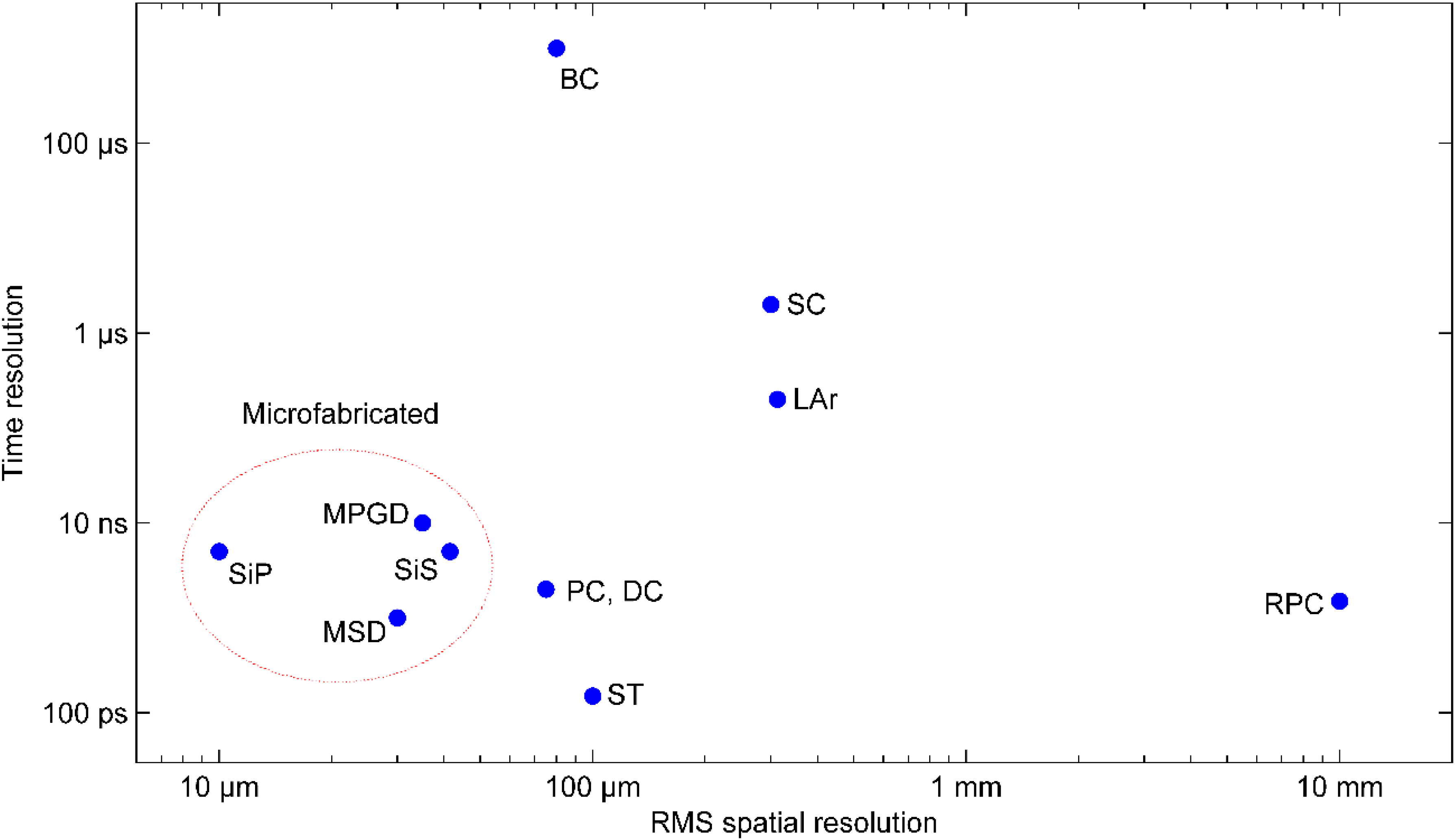
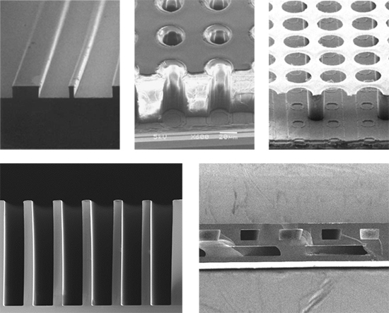
2. Micropattern Gaseous Detectors

In gaseous detectors, the energetic particles pass through a gas-filled volume, ionizing the atoms/molecules along their path. An applied electric field separates the electrons and positive ions created in the gas, and accelerates them in opposite directions. If the electric field is strong enough, the accelerated electrons can induce further ionization in the gas and an avalanche multiplication process occurs. The motion of these charges induces a current in the sensing electrode, providing an output signal for the readout electronics.
Position sensitivity can be achieved with this detection concept by placing several wires (typically at the distance of a few mm) in the gas volume to segment the detector, as it is done in proportional chambers. Another strategy is measuring the arrival time of the electrons to the anodes to infer the interaction position provided the interaction time is known which is the principle exploited in drift chambers. The introduction of modern photolithographic processes led to the development of several micro-pattern gas detectors (MPGD) designs with electrode pitches in the order of 100 μm, allowing improved spatial accuracies (30 μm root mean square) and time resolutions (down to the ns range). Several MPGD structures based on SU-8 have been reported in literature.

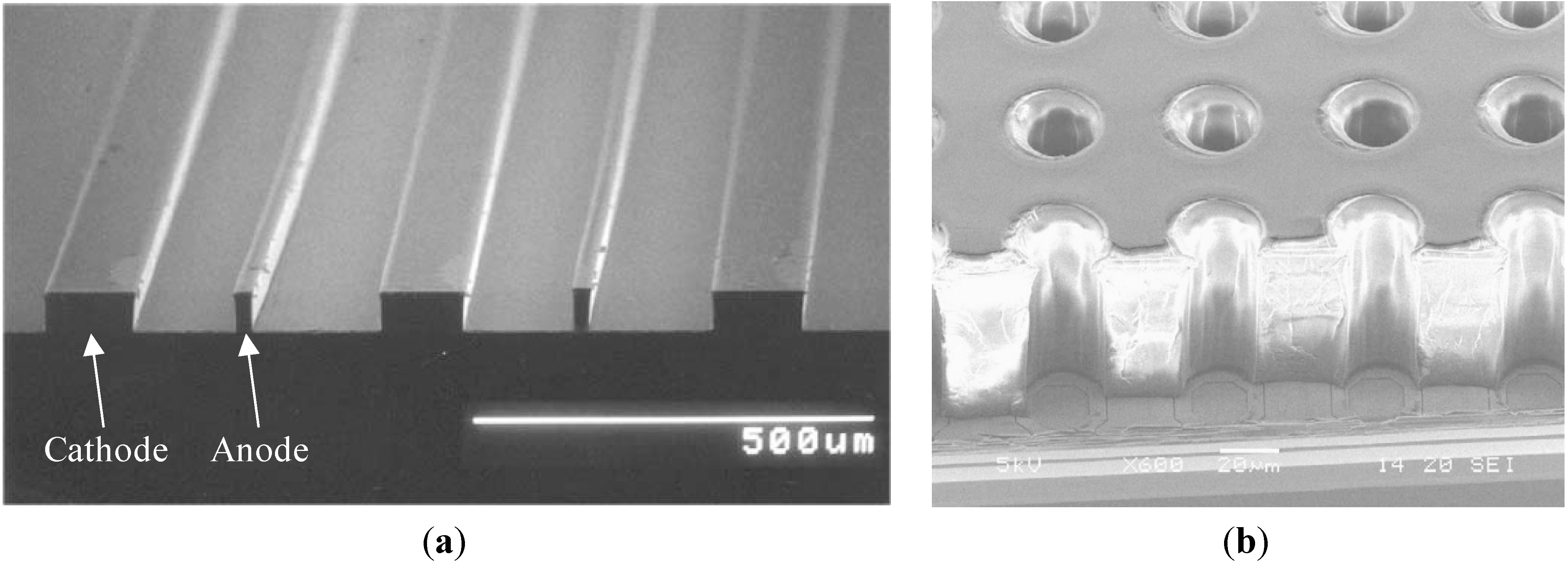
2.1. Microstrip and Microwell MPGDs

In microstrip gaseous detectors (MSGDs) the cathode and anode wires of the traditional chambers are replaced by metal tracks patterned on a generally planar substrate. Non-planar MSGDs in which the electrodes sit on the top of SU-8 strips patterned by photolithography (Figure 2a) were first developed by Key et al. [8]. The anode strip is thinner than the cathode one to generate a locally higher electric field in the surrounding gas, enabling avalanche multiplication of the drifting electrons. The non-planar configuration was chosen to reduce some problems associated to planar MSGDs such as surface charge accumulation and ion migration. This device was also fabricated in a variant with additional electrodes sitting directly on the substrate orthogonally to the SU-8 strips to enable 2D readout sensitivity.
The fabrication process used to obtain such structures consists in the deposition of the first electrode layer (not necessary for the first variant described), coating and exposure (without developing) of a thick SU-8 layer to define the stripes, deposition and patterning by wet etching of the second electrode layer and finally development of the previously exposed SU-8 to obtain the three-dimensional strips.
A similar process was used to produce detectors with a microwell geometry. In this case, the cathode sits on the top the SU-8 layer defining the microwells, while the anode sits on the substrate, i.e., on the bottom of the microwells. The microwell sidewalls obtained through SU-8 photolithography have a better verticality with respect to those obtained for example by polyimide etching, contributing to a higher electric field in the avalanche region inside the well. Microwells made by sandwiching several layers of SU-8 and electrodes can be envisioned to increase the multiplication gain. The CMOS compatibility of this process was demonstrated by Blanco Carballo et al. [9] by fabricating this microwell structure (called by them GEMGrid because of its analogies with Gas Electron Multipliers) directly over an unpackaged Timepix CMOS pixel detector that was used as pixelised anode and readout electronics (Figure 2b).
Figure 2. (a) Scanning electron microscope (SEM) image of basic non-planar microstrip gaseous detectors (MSGD) structure on a glass substrate, sectioned with a wafer saw. Alternated gold anode and cathode electrodes are patterned on top of 50 μm thick SU-8 strips. Adapted from [8], with permission. (b) SEM image of a microwell structure consisting in a 55 μm thick SU-8 layer defining the microwells, with an aluminium top cathode, patterned over a Timepix CMOS chip. Reprinted from [9], © 2004 Elsevier.
Micromachines 05 00594 g002

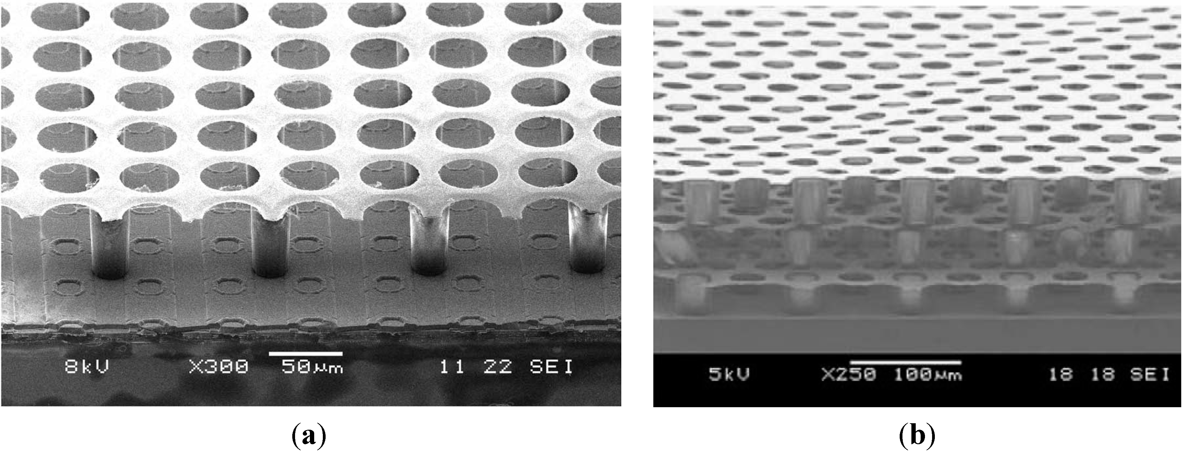
2.2. Micromesh Gaseous Structure Detectors

A different kind of MPGD called micromesh gaseous structure (Micromegas) consists in a thin metallic grid (the micromesh) suspended between cathode and anode electrodes [10]. This electrode structure is spaced and biased in such a way that electrons generated in the ionization gap between the cathode and the micromesh drift towards the latter and are then amplified in the avalanche region present between the micromesh and the anode, thanks to a locally very high electric field generated by the grid geometry.
Chefdeville et al. [11] demonstrated a Micromegas grid built directly on a silicon wafer, suspended by insulating micropillars obtained by SU-8 photolithography. The fabrication steps used to manufacture this structure are similar to the ones described before for the MGSDs. The anode electrodes were deposited and patterned on the substrate, which was then coated with a 50 μm thick SU-8 layer. This layer was exposed (not developed) to define the support micropillars for the micromesh, A relatively thick (0.8 μm) aluminium layer was patterned on top of the SU-8 in order to define the micromesh, prior to developing the SU-8. The so obtained wafer carrying the micromesh suspended over the anode layer was mounted using mechanical spacers at a distance of 10 mm from a metalized Kapton foil, acting as the cathode. Also in this case the micromesh structures could be fabricated directly over unpackaged Medipix2 and Timepix CMOS chips that were used as anodes and readout electronics, thus demonstrating an integrated gaseous-pixel detector (Figure 3a). The possibility of having stacked grid layers to act as multiple electron amplification stages was reported [12]. In this case the bottom layer is produced with the conventional SU-8 coating, exposure, metallization and development process, while for the successive layers spin coating is replaced by hot-roller lamination of uncrosslinked SU-8 films, allowing stacking up to three stages of micromeshes (Figure 3b).
Figure 3. (a) SEM image of an aluminium micromesh grid suspended on top of SU-8 pillars structured in the middle of four pixels of a Medipix2 silicon pixel detector. Reprinted from [13], © 2008 IEEE. (b) SEM image of a triple grid structure. Reprinted from [12], © 2009 Elsevier.
Micromachines 05 00594 g003

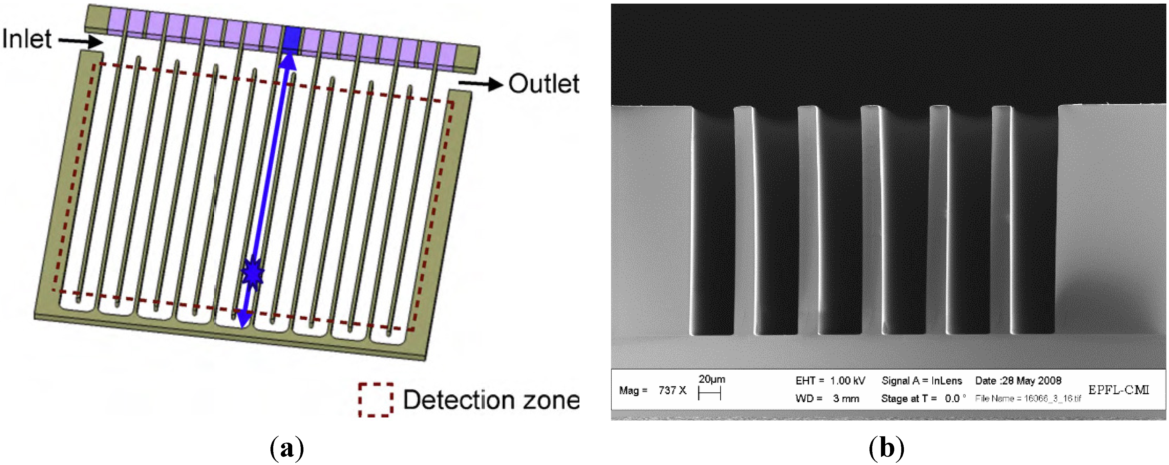
3. Microfluidic Scintillation Detectors

When struck by ionizing radiation, certain materials release a small part of the absorbed energy as optical photons: this phenomenon is called scintillation and such materials are referred to as scintillators. Scintillators can be both inorganic crystals, glasses, gases and organic crystals, polymers and liquids. By combining a scintillator with a photodetector, the light pulses produced in scintillation events can be converted into an electrical signal that conveys information about the incident radiation: such a mechanism constitutes the working principle of scintillation detectors. Position sensitivity can be obtained as usual by segmenting the detector, as is done for example in scintillating fibre detectors, which employ optical fibres with a scintillating core each coupled to its own photodetector (or photodetector pixel).

3.1. Single Layer Devices

As mentioned before, scintillators can be liquid, usually obtained by dissolving an organic scintillator in an organic solvent. When used in a detector they make for an active medium with virtually no radiation aging, as the scintillator can be easily renewed by recirculating new liquid in the detector. Recent advancements in the field of liquid scintillation detectors were made with the introduction of microfluidic scintillation detectors [14]. Such device consists in a single microfluidic channel with a serpentine geometry, patterned by SU-8 photolithography, in which a scintillating liquid is injected. The walls of the microchannel are gold coated, so that it defines a series of parallel, optically independent, mirror waveguides. The channel end is left uncoated so that light can be transmitted through the SU-8 wall (which exhibits high transparency for light around the 425 nm wavelength [4], corresponding to the peak emission of most liquid scintillators). In this way the light generated in the liquid by scintillation is guided along the channel until it is captured by the corresponding pixel of a pixelated photodetector in contact with the chip (Figure 4a). With this readout scheme the position (in one dimension) of the particle can be determined. Photodetectors such as photomultiplier tubes (PMTs), silicon photomultipliers (SiPMs) or photodiodes can be used for the light readout, depending on the needs of the particular application addressed.
The reported device has a microchannel pitch of 60 μm in the detection zone, leading to a high spatial resolution (17 μm RMS). The high aspect ratio capabilities of SU-8 allowed to obtain narrow channel walls over a depth of 200 μm (Figure 4b), enabling a high fill-factor while keeping enough liquid thickness to produce and guide a light pulse with an efficacy comparable to small diameter scintillating fibres [15]. Thanks to the single-channel configuration, it is relatively easy to replace the liquid scintillator in the device, resulting in an increased radiation resistance.
Figure 4. (a) Schematic representation of a microfluidic scintillation detector (adapted from [14], with permission). A single microfluidic channel defines an array of optically separated waveguides. When a particle interacts with the liquid scintillator in one of the branches, the scintillation light is guided towards the corresponding photodetector pixel. (b) SEM image of a device cross section in the detection zone, showing the very high aspect ratio microfluidic channels.
Micromachines 05 00594 g004

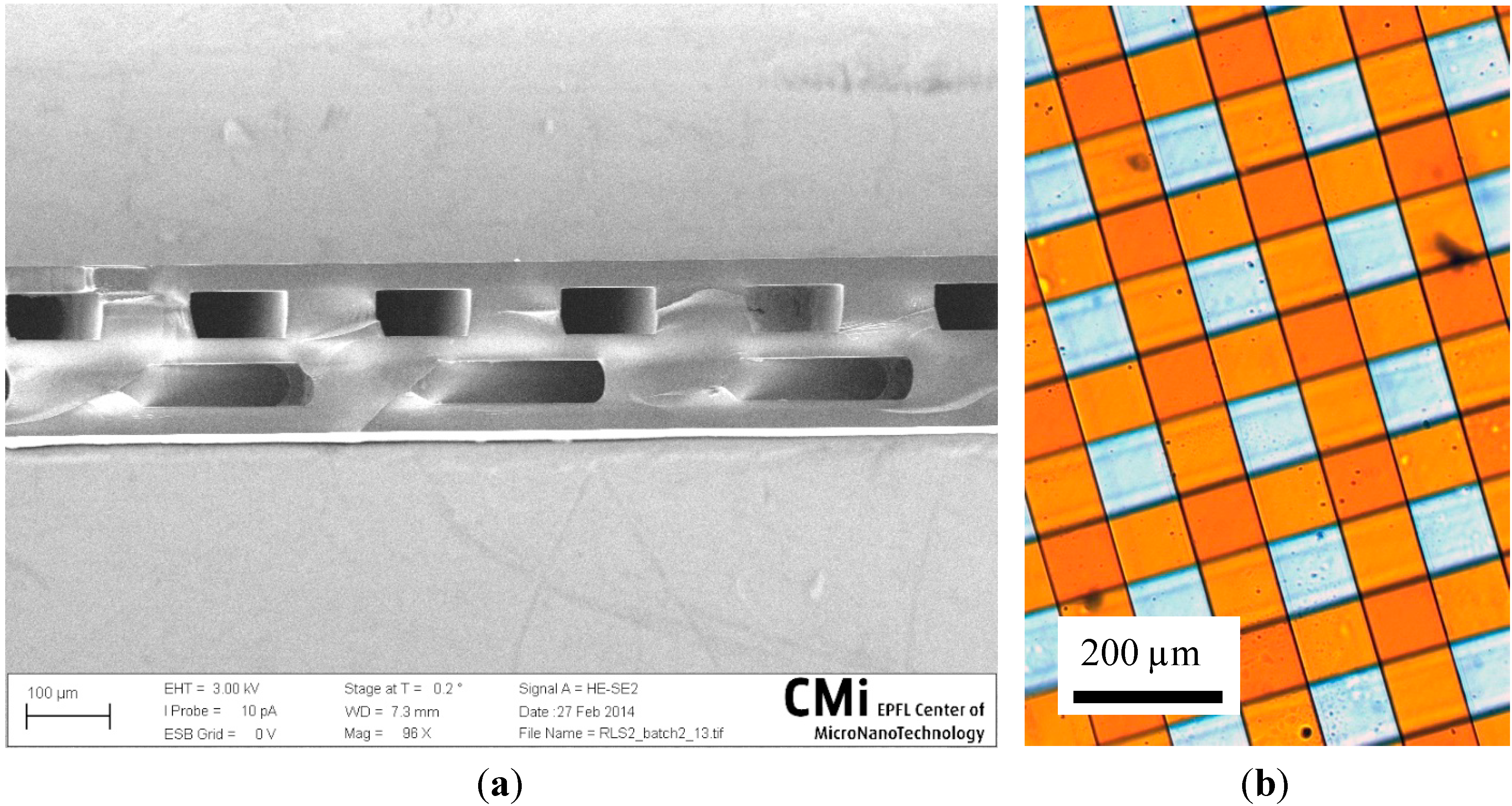
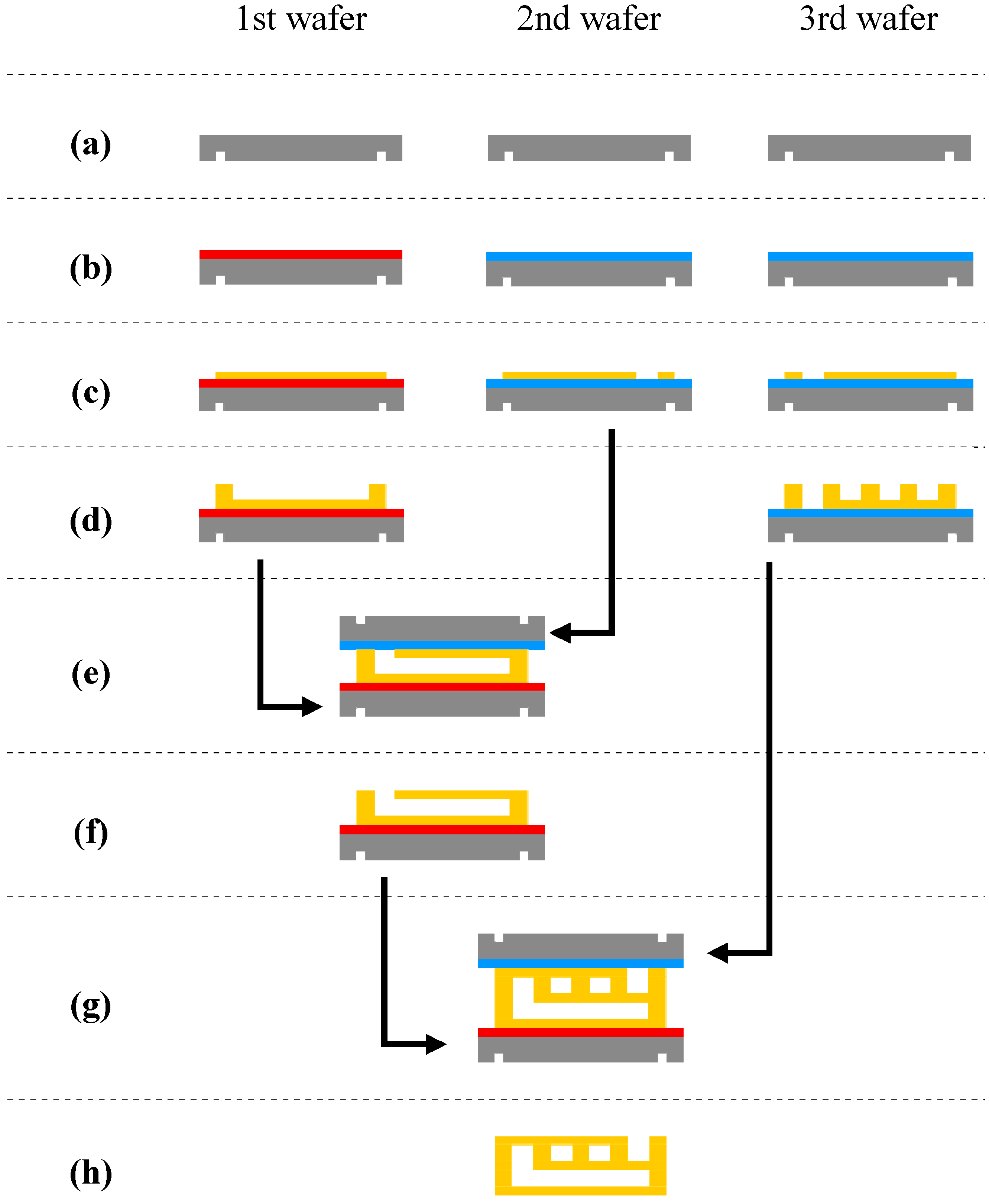
3.2. Towards Two Dimensional Position Sensitivity

With one layer of microchannels, the position of the interaction in one dimension can be measured. By stacking a second layer of microchannels orthogonal to the first one, a second coordinate is obtained, so that it is possible to determine the (x,y) position of the interaction on the detector plane [16]. Such characteristic is not only desirable in particle tracking, but also in other applications such as beam profiling, meaning the reconstruction of the energy distribution in a beam cross section. In this case a high number of particles continuously pass through the detector, and a light signal proportional to the local flux is produced. Scintillation detectors are believed to be particularly suited for this task because of the intrinsic radiation resistance enabled by the use of a liquid scintillator, as discussed before. In monitoring, spatial resolution is less important than in tracking as the energy distribution along the beam cross section does not generally present sharp spatial variations meaning that a very dense spatial sampling of the beam is not needed and thus extremely narrow microchannels are not necessary. However, in specific monitoring applications, it is essential to limit the thickness of the detector in order to reduce as much as possible any perturbation (scattering, absorption) induced by the detector inserted in the beam line. In this section we report on recent work that has been done in this direction for the integration of two layers of microchannels in SU-8 microfluidic scintillation detectors.
Three silicon wafers were dry-etched to pattern reference alignment marks on the backside (Figure 5a). A 50 nm thick chromium sacrificial film was deposited on the first wafer, while 50 nm of aluminium were used for the other two (Figure 5b). A 30 μm thick SU-8 layer (GM1070 from Gersteltec, Pully, Switzerland) was patterned over the metalized substrates with a standard photolithographic procedure, defining the bottom part of the devices on the chromium-coated wafer while the middle and and top parts of the devices were structured on the aluminium-coated wafers (Figure 5c). A thicker (50 μm) SU-8 layer was then coated on the wafers carrying the bottom and top parts, and patterned to define the microchannel walls for the bottom and top microfluidic layers (Figure 5d). For all these photolithographies, the soft bake, the UV exposure dose, the post-exposure bake temperature and duration, as well as the development steps, were optimised in order to keep into account the high reflectivity of the metallic sacrificial layers and to limit the stress build up. These parameters were found to be important for the success of the subsequent steps, as having overly crosslinked or stressed SU-8 layers would result in respectively bonding failure or warped microstructures after release. The soft bake for both the 30 and 50 μm layers were performed 10 min after the spin coating, by ramping up from 20 to 120 °C in 25 min (4 °C·min−1) then promptly ramping down again to 20 °C at the same rate. Good results could be consistently obtained using an exposure dose of 80 mJ·cm−2, followed by a 40 min bake at 90 °C and 3 min of development in propylene glycol monomethyl ether acetate (PGMEA), for 30 μm thick SU-8 layers. A dose of 120 mJ·cm−2 followed by the same post-exposure bake and 5 min of development in PGMEA were found suitable for 50 μm thick layers. These parameters were also found to be largely independent from the geometrical pattern used. With this choice of thicknesses, all the photolithographic steps could be conveniently grouped in two batches sharing the same exposure and bake conditions, thus limiting the processing time.
The bottom and middle wafers were aligned using the reference marks etched on the backside and put in contact before bonding using a Suss MA6/BA6 system. Full wafer bonding of the SU-8 layers to assemble the microstructures together was performed in a Suss SB6 bonder, applying a pressure of 4 bars at 125 °C for 1.5 h (Figure 5e). The bonded wafer sandwich was then put in AZ400K developer (a low concentration KOH solution) in order to selectively dissolve the aluminium sacrificial layer, thus releasing the middle layer from its carrier (Figure 5f). A mild but continuous ultrasonic agitation was used to remove the hydrogen bubbles forming at the interface, which could otherwise slow down or stop the dissolution reaction. In this way a chromium-coated silicon substrate carrying embedded microfluidic channels made by three-layers of SU-8 was obtained. A further full wafer alignment and bonding step was performed to assemble the two top parts, thus forming the second microfluidics layer and completing the devices (Figure 5g). In this case the bonding temperature was raised to 155 °C in order to keep into account the increased crosslinking of SU-8 induced in the first three layers by the previous bonding. This temperature is also sufficient to thermally activate any unreacted photoinitiator molecule that may still be present, so that the resin is fully crosslinked at the end of the process. The devices were finally released by dissolving both the aluminium and chromium sacrificial layers by putting the wafer sandwich in a 34% HCl solution, then rinsed with DI water and vacuum dried (Figure 5h). This process allowed obtaining 200 μm thick, free-standing SU-8 chips with two orthogonal layers of microfluidic channels (Figure 6a). The chips were filled with a colorant to test the fluidic operation (Figure 6b). The width and pitch of the microchannels can be adjusted to match the photodetector array of choice. Current investigation is focused on the addition of a suitable optical coating to the microchannels.
Figure 5. Process flow for the fabrication of thin double layer SU-8 microfluidic devices. (a) Etching of alignment marks on the backside of three wafers; (b) Deposition of metallic sacrificial layers, chromium for the first wafer and aluminium for the other two; (c) Photolithographic patterning of SU-8 bottom, middle and top part, including fluidic vias and inlets; (d) Photolithographic patterning of bottom and top microchannel walls; (e) Bonding of bottom and middle parts; (f) Selective release from middle layer carrier wafer; (g) Bonding to top part to complete the assembly; (h) Release from the carrier wafers to obtain a self-standing device.
Micromachines 05 00594 g005
Figure 6. (a) SEM image showing an oblique cross section of the 200 μm thick, monolithic SU-8 chips integrating two microchannel layers. The microchannels are 100 μm wide and 50 μm deep, while the pitch is 200 μm. These dimensions were chosen to match the pixel positions of the Hamamatsu (Hamamatsu, Japan) S8866-128-02 photodiode arrays. (b) Optical micrograph from the top showing the same microchannel network filled with a colorant.
Micromachines 05 00594 g006

4. Applications Overview

In order to provide a panorama of the interesting applications being studied for the detector technologies previously described, we report here on selected examples, without any ambition of completeness.

4.1. Particle Tracking in High-Energy, High-Luminosity Experiments

The currently running COMPASS experiment at the CERN Super Proton Synchrotron (SPS) was the first high-energy physics experiment to use Micromegas tracking detectors. The COMPASS setup consists in a fixed target on which a muon beam is directed, and a series of detectors downstream that analyse the collision products. Four planes of Micromegas detectors sit directly behind the target as part of a large angle spectrometer, and are used to track particles coming at a high rate from the target (up to 450 kHz·cm−2 in the zones closer to the beam axis). Performance measurements performed during the 2002–2004 data-taking period showed a mean time resolution of 9.3 ns and a spatial resolution of 90 μm. No performance loss in time was observed, indicating good radiation resistance/ageing properties of the Micromegas [17]. Because of the excellent performance demonstrated by Micromegas, especially in terms of rate capability, the ATLAS experiment at the CERN Large Hadron Collider (LHC) has chosen to introduce them in the upgrades of its Muon Spectrometer, in particular in the first endcaps of the forward region (Muon Small Wheels) where the particle rate is expected to go up to 1034 Hz·cm−2 following the High Luminosity LHC upgrade [18]. The large size Micromegas necessary for this application will be manufactured replacing SU-8 photolithography with technologies based on the lamination of photosensitive dry-films such as Vacrel [19,20].

4.2. β Autoradiography Imaging and Liquid Scintillation Counting

The β autoradiography is a technique used in pharmacology and genetics to image the distribution of molecules labelled with 3H or 14C radioactive markers in biological tissues, by detecting the electrons emitted by β decay. Traditionally emulsion films or phosphor screens are used for the image production, but are limited by their exposition time and do not allow any adjustment of the image during acquisition. The use of a variant of Micromegas called Parallel Ionisation Multipliers (PIMs) for faster β imaging is reported in literature. In this application, the tissue sample containing the marked molecules sits on a glass slide directly over the detector, which amplifies and detects the emitted electrons. Good efficiencies (50% to 85% depending on the radioactive marker [21]) and two dimensional spatial resolutions (27 μm FWHM (Full Width Half Maximum) [22]) were demonstrated.
A similar application is liquid scintillation counting, in which biological fluids are mixed with a scintillator cocktail to determine the presence of 3H or 14C marked molecules by detecting the optical photons emitted by scintillation. Thanks to their reduced internal volume, scintillation detectors based on microfluidic channels could provide a straightforward method for performing this kind of analysis on small volume liquid samples with high sensitivity.

4.3. On-Line Beam Monitoring in Hadron Therapy

Hadron therapy is a medical technique consisting in the irradiation of otherwise difficult to reach tumours with a hadron beam (typically protons or carbon ions with energies in the order of 10–100 MeV), resulting in the death of the cancerous cells. The use of hadrons entails an advantage with respect to classical radiotherapy, because while X-rays deposit energy in the tissues gradually along all the tissue thickness, the energy of the hadrons can be tuned so that almost all the energy deposit occurs at a specific depth in the tissue (at the so called Bragg peak), meaning that much less damage is caused to the healthy tissues surrounding the tumour.
For obvious safety reasons, a precise control of the particle team size and profile (energy distribution along the cross section) is necessary for this application. The traditional detection technologies used for these measurements require the treatment to stop during the beam characterization, because of the perturbation introduced by the detector itself (scattering, absorption), mostly because of its thickness. Microfluidic scintillation detectors seem to be good candidates for the implementation of on-line beam monitors that can measure the beam profile in real time during the treatment of the patient, providing a more accurate control. This is because of both the very limited thicknesses that it is possible to reach with these devices and the increased radiation resistance resulting from the use of liquid scintillators that can be easily replaced during operation by pumping, as discussed in Section 3. Moreover the detector configuration is such that only the microchannels are directly hit by the beam, while the photodetectors for the scintillation light readout sit on the sides of the active area, thus receiving a much lower radiation dose.

5. Conclusions

We provide a summary of emergent detector technologies for particle physics based on SU-8 microstructures. These can be split in two main families, based respectively on gas ionization and liquid scintillation. In MPGDs, which include devices such as microstrips, microwells and micromegas, SU-8 is used to pattern electrically insulating microstructures, which act as supports for metallic electrodes biased with high voltages and immersed in a gaseous atmosphere. In microfluidic detectors, SU-8 is used as a structural material for the microfluidic channels and also as an optical material for the transparent zones where the microchannels are in contact with a photodetector. A novel process based on multiple bonding and release steps for the fabrication of thin monolithic SU-8 devices with two layers of microchannels was presented, in the context of the development of microfluidic scintillation detectors with 2D position sensitivity for particle tracking and beam monitoring applications. A brief overview of the new applications being studied for Micromegas and microfluidic scintillation detectors was given, showing how these technologies can be employed not only in experimental particle physics, but also in the biological and medical fields.

Acknowledgments

We would like to acknowledge Arnaud Bertsch for his advice in the manuscript revision.

Author Contributions

Pietro Maoddi developed the reported process for SU-8 double layer microfluidic devices and wrote the manuscript. Alessandro Mapelli developed the single layer microfluidic scintillation detectors, supervised the work and reviewed the manuscript. Sebastien Jiguet provided support on SU-8 processing and reviewed the manuscript. Philippe Renaud supervised the work and reviewed the manuscript.

Conflicts of Interest

The authors declare no conflict of interest.

References

  1. Beringer, J.; Arguin, J.F.; Barnett, R.M.; Copic, K.; Dahl, O.; Groom, D.E.; Lin, C.J.; Lys, J.; Murayama, H.; Wohl, C.G.; et al. Review of particle physics. Phys. Rev. D. 2012, 86. [Google Scholar] [CrossRef]
  2. Lorenz, H.; Despont, M.; Fahrni, N.; LaBianca, N.; Renaud, P.; Vettiger, P. SU-8: A low-cost negative resist for MEMS. J. Micromech. Microeng. 1997, 7, 121–124. [Google Scholar] [CrossRef]
  3. Lee, C.H.; Jiang, K.; Davies, G.J. Sidewall roughness characterization and comparison between silicon and SU-8 microcomponents. Mater. Charact. 2007, 58, 603–609. [Google Scholar] [CrossRef]
  4. Kuo, J.N.; Wu, H.W.; Lee, G.B. Optical projection display systems integrated with three-color-mixing waveguides and grating-light-valve devices. Opt. Express 2006, 14, 6844–6850. [Google Scholar] [CrossRef] [PubMed]
  5. Melai, J.; Salm, C.; Smits, S.; Visschers, J.; Schmitz, J. The electrical conduction and dielectric strength of SU-8. J. Micromech. Microeng. 2009, 19. [Google Scholar] [CrossRef]
  6. Melai, J.; Salm, C.; Wolters, R.; Schmitz, J. Qualitative and quantitative characterization of outgassing from SU-8. Microelectron. Eng. 2009, 86, 761–764. [Google Scholar] [CrossRef]
  7. Key, M.J.; Cindro, V.; Lozano, M. On the radiation tolerance of SU-8, a new material for gaseous microstructure radiation detector fabrication. Radiat. Phys. Chem. 2004, 71, 1003–1007. [Google Scholar] [CrossRef]
  8. Key, M.J.; Llobera, A.; Lozano, M.; Ramos-Lerate, I.; Seidemann, V. Fabrication of gas amplification microstructures with SU-8 photosensitive epoxy. Nucl. Instr. Meth. A 2004, 525, 49–52. [Google Scholar] [CrossRef]
  9. Blanco Carballo, V.M.; Bilevych, Y.; Chefdeville, M.; Fransen, M.; van der Graaf, H.; Salm, C.; Schmitz, J.; Timmermans, J. GEMGrid: A wafer post-processed GEM-like radiation detector. Nucl. Instr. Meth. A 2009, 608, 86–91. [Google Scholar]
  10. Giomataris, Y.; Rebourgeard, P.; Robert, J.P.; Charpak, G. Micromegas: A high-granularity position-sensitive gaseous detector for high-particle-flux environments. Nucl. Instr. Meth. A 1996, 376, 29–35. [Google Scholar] [CrossRef]
  11. Chefdeville, M.; Colas, P.; Giomataris, Y.; van der Graaf, H.; Heijne, E.H.M.; van der Putten, S.; Salm, C.; Schmitz, J.; Smits, S.; Timmermans, J.; et al. An electron-multiplying “Micromegas” grid made in silicon wafer post-processing technology. Nucl. Instr. Meth. A 2006, 556, 490–494. [Google Scholar] [CrossRef]
  12. Bilevych, Y.; Blanco Carballo, V.M.; Chefdeville, M.; Fransen, M.; van der Graaf, H.; Salm, C.; Schmitz, J.; Timmermans, J. TwinGrid: A wafer post-processed multistage micro patterned gaseous detector. Nucl. Instr. Meth. A 2009, 610, 644–648. [Google Scholar] [CrossRef]
  13. Blanco Carballo, V.M.; Chefdeville, M.; Fransen, M.; van der Graaf, H.; Melai, J.; Salm, C.; Schmitz, J.; Timmermans, J. A radiation imaging detector Made by postprocessing a standard CMOS chip. IEEE Electron Device Lett. 2008, 29, 585–587. [Google Scholar]
  14. Mapelli, A.; Gorini, B.; Haguenauer, M.; Jiguet, S.; Lehmann Miotto, G.; Vandelli, W.; Vico Triviño, N.; Renaud, P. Scintillation particle detection based on microfluidics. Sensors Actuators A Phys. 2010, 162, 272–275. [Google Scholar] [CrossRef]
  15. Mapelli, A. Scintillation Particle Detectors Based on Plastic Optical Fibres and Microfluidics. Ph.D. Thesis, École Polytechnique Fédérale de Lausanne, Lausanne, Switzerland, 2011. [Google Scholar]
  16. Mapelli, A.; Maoddi, P.; Renaud, P. Microfabricated scintillation detector. WIPO Patent 2013167151 A1, 14 November 2013. [Google Scholar]
  17. Abbon, P.; Albrecht, E.; Alexakhin, V.Y.; Alexandrov, Y.; Alexeev, G.D.; Alekseev, M.G.; Amoroso, A.; Angerer, H.; Anosov, V.A.; Badełek, B.; et al. The COMPASS experiment at CERN. Nucl. Instr. Methods A 2007, 577, 455–518. [Google Scholar] [CrossRef] [Green Version]
  18. Gemme, C. The ATLAS Upgrade Programme. In Proceedings of the 20th International Workshop on Deep-Inelastic Scattering and Related Subjects, Bonn, Germany, 26–30 March 2012.
  19. Giomataris, I.; de Oliveira, R.; Andriamonje, S.; Aune, S.; Charpak, G.; Colas, P.; Fanourakis, G.; Ferrer, E.; Giganon, A.; Rebourgeard, P.; et al. Micromegas in a bulk. Nucl. Instr. Methods A 2006, 560, 405–408. [Google Scholar] [CrossRef]
  20. Alexopoulos, T.; Altintas, A.A.; Alviggi, M.; Arik, M.; Cetin, S.A.; Chernyatine, V.; Cheu, E.; Della, D.; Volpe, M.; Dris, D.; et al. Development of large size micromegas detector for the upgrade of the ATLAS muon system. Nucl. Instr. Methods A 2010, 617, 161–165. [Google Scholar] [CrossRef]
  21. Samarati, J.; Charpak, G.; Coulon, P.; Leguay, M.; Leray, P.; Lupone, S.; Luquin, L.; Metivier, V.; Meynadier, M.; Morteau, E.; et al. β-Imaging with the PIM device. Nucl. Instr. Methods A 2004, 535, 550–553. [Google Scholar]
  22. Donnard, J.; Thers, D.; Servagent, D.; Luquin, S. High spatial resolution in β-imaging with a PIM device. IEEE Trans. Nucl. Sci. 2009, 56, 197–200. [Google Scholar] [CrossRef]

