A Bi-Directional Out-of-Plane Actuator by Electrostatic Force

1
School of Electrical, Computer and Energy Engineering, Arizona State University, Tempe, AZ 85287, USA
2
State Key Lab of Optical Technologies for Microfabrication, Institute of Optics and Electronics, Chinese Academy of Sciences, Chengdu 610209, China
*
Author to whom correspondence should be addressed.
Micromachines 2013, 4(4), 431-443; https://doi.org/10.3390/mi4040431
Submission received: 1 July 2013
/
Revised: 21 August 2013
/
Accepted: 30 October 2013
/
Published: 5 December 2013
Abstract
:Presented in this paper is a bi-directional out-of-plane actuator which combines the merits of the electrostatic repulsive principle and the electrostatic attractive principle. By taking advantage of the electrostatic repulsive mode, the common “pull-in” instability can be lessened to enlarge the displacement, and by applying the electrostatic attractive mode, the out-of-plane displacement is further enlarged. The implications of changing the actuator’s physical dimensions are discussed, along with the two-layer polysilicon surface microfabrication process used to fabricate such an actuator. The static characteristics of the out-of-plane displacement versus the voltage of both modes are tested, and displacements of 1.4 μm and 0.63 μm are obtained at 130 V and 15 V, respectively. Therefore, a total stroke of 2.03 μm is achieved, more than 3 fold that of the electrostatic attractive mode, making this actuator useful in optical Micro-Electro-Mechanical Systems (MEMS) and Radio Frequency (RF) MEMS applications.
1. Introduction
Currently, MEMS (Micro-Electro-Mechanical Systems) out-of-plane actuators have been a key component in optical and RF MEMS applications due to their small footprint, batch fabrication, low expense, and beneficial mechanical characteristics [1,2,3,4,5,6,7,8]. Unlike electromagnetic, piezoelectric, and electrothermal out-of-plane actuators [9,10,11,12], MEMS electrostatic actuators offer a smaller footprint, lower power consumption, and a faster response time.
An out-of-plane actuator’s stroke, or maximum displacement, is critical for its application, e.g., when implemented as part of a spatial light modulator in adaptive optics systems, the larger the stroke, the larger amplitude of wavefront phase aberrations can be corrected [13]. However, conventional electrostatic out-of-plane actuators that utilize the electrostatic attractive force suffer from a major drawback: “pull-in” instability causes the stroke to be at most one-third of the initial gap between electrodes. Therefore, for an actuator with an initial gap of 2 μm between electrodes, the stroke can approach at most 0.67 μm [14].
Several attempts have been made to increase displacement in order to meet the demands of many micro-mirrors and micro-capacitors. These methods include using thicker sacrificial layers, introducing an insulation layer between the top and bottom electrodes, using self-assembly to levitate the initial gap, and applying leverage structures to amplify the stroke [15,16,17,18,19,20,21,22]. However, these approaches require difficult fabrication processes or suffer from structural complexity. Lee et al., He et al. and Yao et al., designed an out-of-plane actuator that eliminates the “pull-in” instability—thereby enlarging stroke—by means of the electrostatic repulsive force [23,24,25]. Prior-art in our group also implemented either electrostatic attractive force or leverage structure for out-of-plane actuator design, the maximum displacement, 1.4 µm [14,21]. Although this maximum displacement is enough for correcting wavefront aberration in visible light wavelength range (400–700 nm), it is still not enough for near infra-red range.
In order to enlarge the maximum displacement, we integrate electrostatic repulsive mode and electrostatic attractive mode to present a novel bi-directional out-of-plane actuator that maximizes displacement due to the integrated displacement generated by the sum of the two modes. The actuator of this work is capable of generating a 2 µm maximum displacement that meets adaptive optics systems application, and may also be used in other optical and RF MEMS applications. The manuscript is organized as follows: in the second section, the structure and operation principle of the bi-directional out-of-plane actuator is presented; in the third section, the characteristics of the actuator are discussed, mainly the influence of the dimensions on the displacement of the actuator; finally, the fabrication and test results are demonstrated.
2. Structure and Operation Principle
2.1. Structure of a Novel Bi-Directional Out-of-Plane Actuator
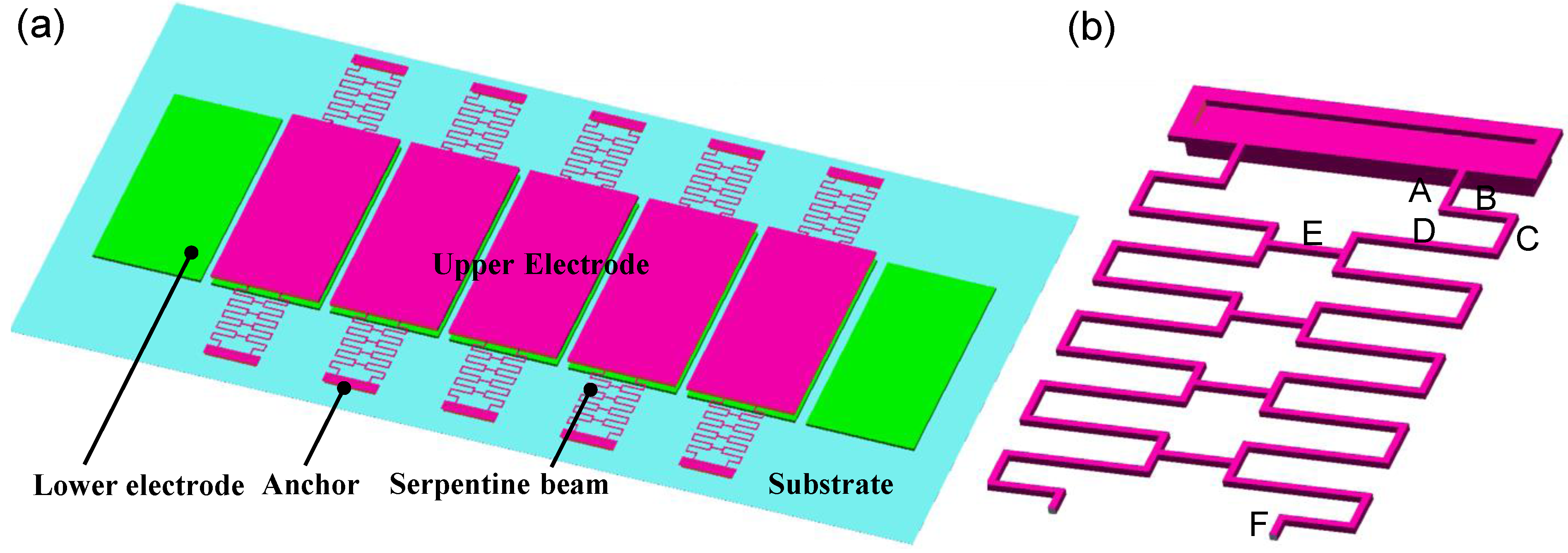
By combining the electrostatic repulsive and attractive force, a novel bi-directional out-of-plane actuator is designed to enlarge the maximum out-of-plane displacement, as depicted in Figure 1a. The actuator consists of two layers parallel to each other. The top layer, made of 2 µm thick polysilicon, is composed of mirror plates (also serving as upper electrodes), serpentine beams and anchors. The bottom layer, which is 0.5 µm thick polysilicon, is composed of the lower electrodes. On each side of the mirror plates there is one suspension beam connecting the mirror with the anchor. The anchors and lower electrodes are fixed to the substrate.
Figure 1.
(a) Lateral view of the out-of-plane actuator schematic. Cyan represents the substrate layer, green represents the first polysilicon layer (bottom layer), pink represents the second polysilicon layer (top layer); (b) Lateral view of the serpentine beams on the second polysilicon layer, A–F illustrate different segments for structural parameters.

As shown in Figure 1b, the serpentine beams are thin and folded. By using a thin serpentine beam, a relatively small flexible stiffness is obtained in the out-of-plane direction, thus achieving a larger displacement when using the same force. As depicted in reference [26], by applying this folded serpentine beam, the first resonant mode can be the piston mode, making this actuator robust.
2.2. Operation Principle
In this section, we describe the operation principle of the out-of-plane actuator, including electrostatic repulsive mode and electrostatic attractive mode.
2.2.1. Electrostatic Repulsive Mode
The operation principle of the electrostatic repulsive mode is illustrated in Figure 2. Figure 2a shows the arrangement of electrodes and the voltage application type which can achieve electrostatic repulsive force. When the electrodes on the same layer are subjected to different alternating potentials, one grounded and the other subjected to a positive voltage, and the lower electrodes have the same potential with the upper electrode right above it, an asymmetric electrostatic field will be generated. FEA simulation of the distribution of electrical field when V = 100 V is shown in Figure 2b. From Figure 2a,b, we observe that the magnitude of electric field at the top surface is stronger than the corresponding point at the bottom surface, thus the electrostatic force produced on the top surface of the upper electrode will be stronger than that of the corresponding point on the bottom surface (Figure 2c), resulting in a net repulsive force between upper and lower electrodes. After this repulsive force is generated, as the lower electrodes are all fixed to the substrate, and the upper electrodes are suspended by the serpentine beams, the upper electrodes will be pushed up, thus resulting in the electrostatic repulsive mode.
Figure 2.
Schematic of generation of electrostatic repulsive force: (a) Arrangement of electrode and application of voltage on different electrodes to generate electrostatic repulsive force, here “V” indicate the application of a positive voltage to this electrode and “GND” means application of ground; (b) Simulated cross-sectional magnitude of the electrostatic field of the structure in this paper, when V = 100 Volts, based on simulation, schematic of electrical field distribution of the two central electrodes are given in Figure 2a; (c) Schematic of force distribution of the upper central electrode, as shown inside dashed line.
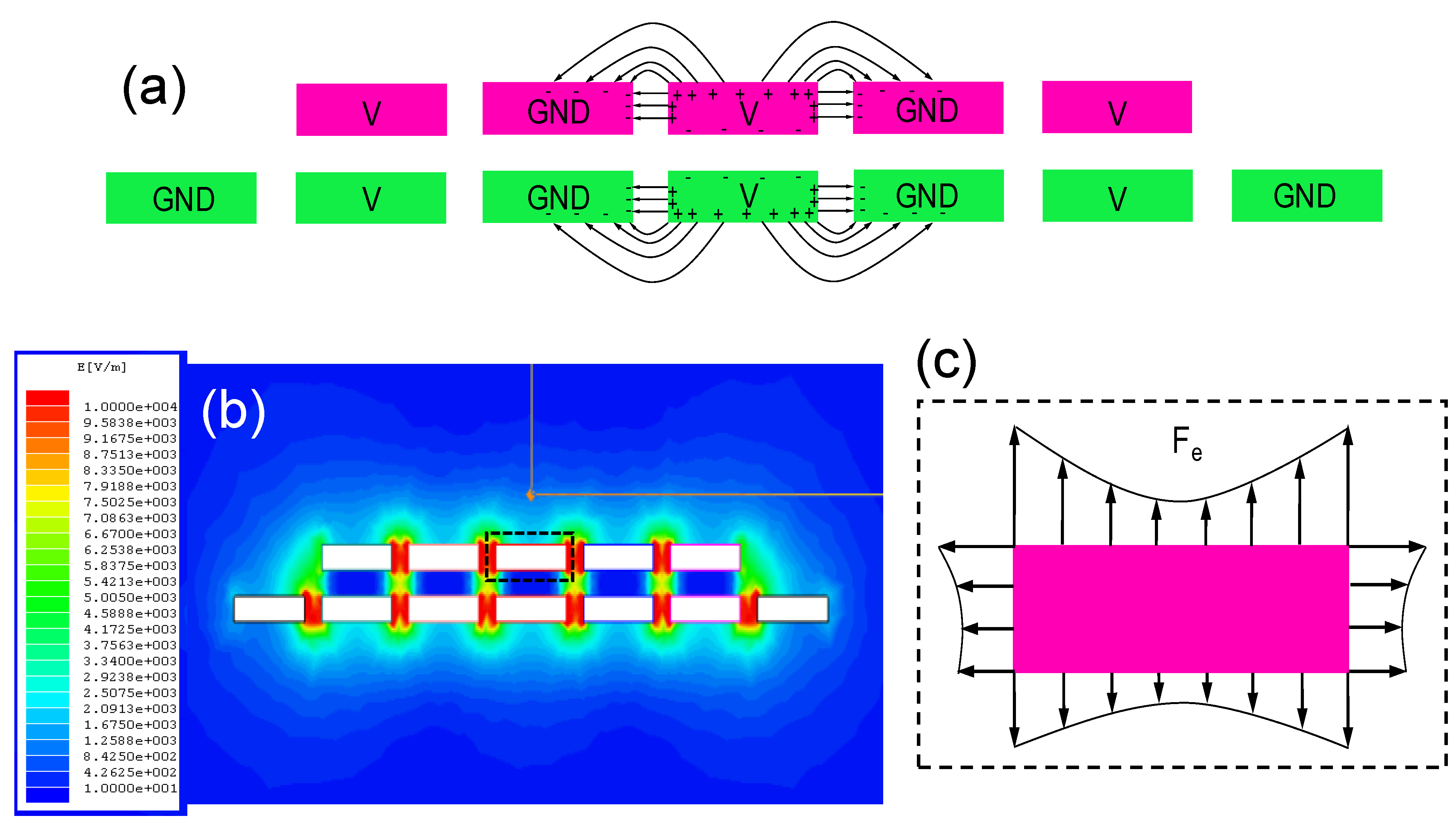
It should be noted that the electrodes at the two sides of the central electrode are essential to generate the electrostatic repulsive force, because it is these electrodes that create the asymmetric electric field to make the electric field at the top surface of the central upper electrode higher than bottom surface, which results in the electrostatic repulsive force. If the electrodes at the two sides are removed, and only central electrodes are applied to the same positive voltage, the electric field at the top and bottom surface are both very small (because there is no ground, and we assume ground is infinite far from these two electrodes); therefore, no repulsive force is generated.
The advantage of electrode arrangement and the voltage application type in Figure 2, compared with Figure 3 of our previous publication [14,25,26], is that by applying the same voltage, a larger electrostatic repulsive force is obtained. It can be seen clearly that electrical field at the top surface of the central electrode for Figure 2b is larger than Figure 3b (dashed rectangular region), resulting in a larger repulsive force, which is helpful to obtain a larger displacement at the same applied voltage.
Figure 3.
(a) Arrangement of electrode and application of voltage on different electrode to generate electrostatic repulsive force in prior art presented by our group [14,25,26]; (b) Simulated cross-sectional magnitude of the electrostatic field of the structure in a, when V = 100 Volts; Compared with Figure 3b (dashed rectangular region), electric field at the top face of central electrode in Figure 2b is larger, resulting in a larger electrostatic repulsive force.

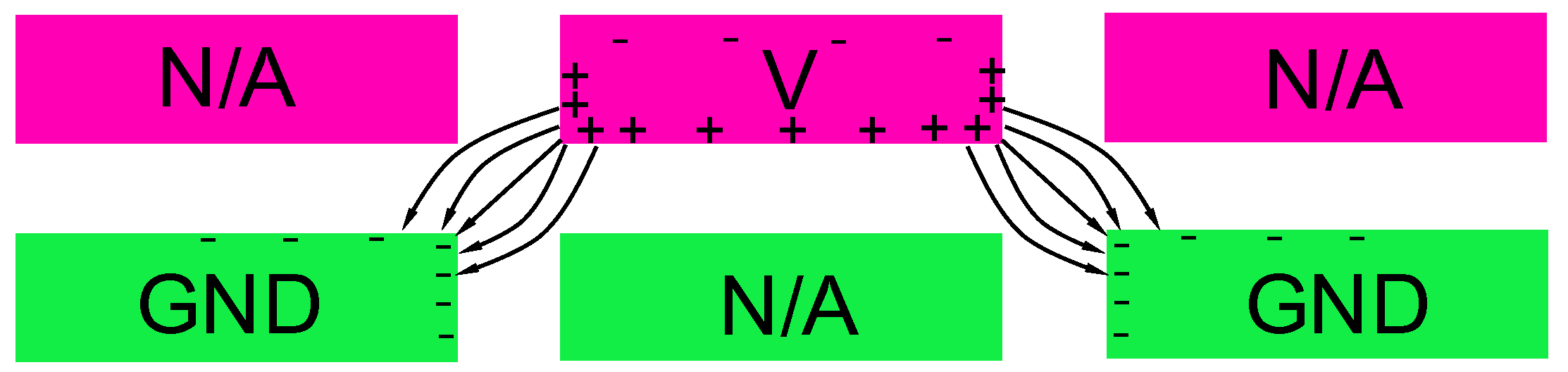
2.2.2. Electrostatic Attractive Mode
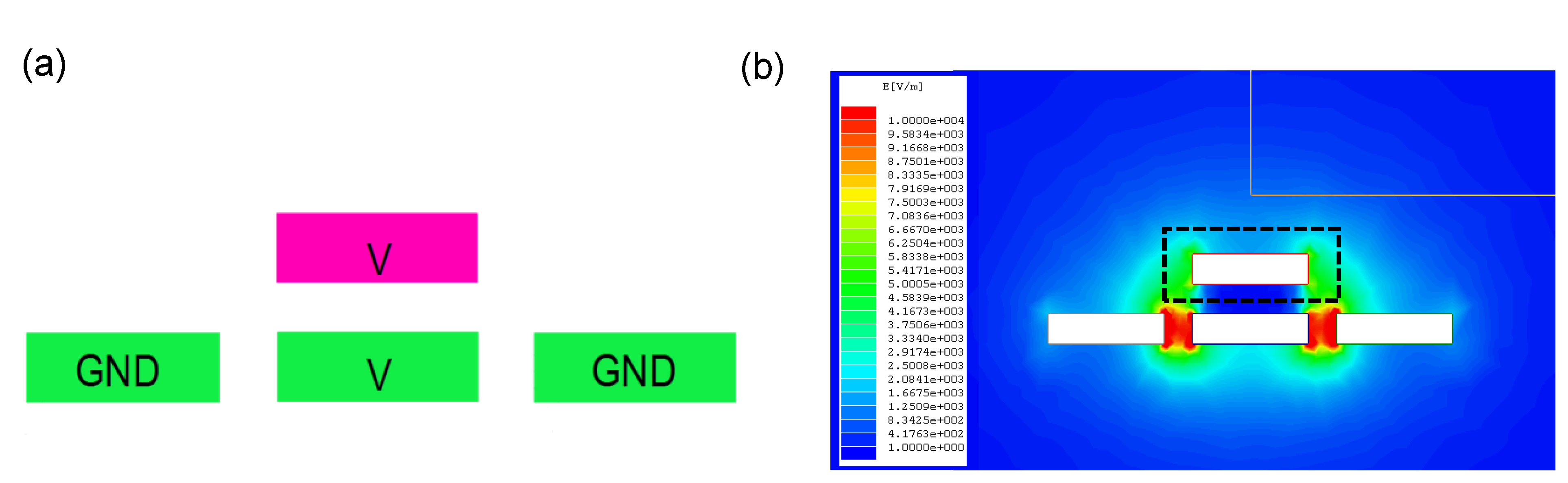
In the electrostatic attractive mode, the application of voltage is shown in Figure 4. Different potentials are applied to the upper and lower electrodes. The central electrode on the top layer is applied a positive voltage and the two electrodes at two sides in the bottom layer are grounded, as depicted in Figure 4. Here, no voltage is applied to the lower electrode right beneath the upper electrode. There are two reasons for this. The first one is to avoid the “pull-in” instability when only a small voltage is applied (less than 1 V based on simulation), which makes the actuator difficult to control. The second reason is, even when “pull-in” occurs, the device will not short-circuit (even when the central electrode on the top layer suffers from pull-in instability and contacts with the electrode right beneath, short-circuiting does not occur, because the electrode right beneath the central electrode on the top electrode is floating), which makes the device robust. When the actuator works in the electrostatic attractive mode, it is obvious that an electrostatic attractive force arises between the central electrode on the top layer and the two lower electrodes and central electrode on the top layer is pulled down.
Figure 4.
Schematic of the electrostatic attractive mode (cross-sectional view, only the three pairs of electrode in the center is shown); here “V” indicates the application of a positive voltage to this electrode, “GND” means application of ground, and N/A indicates electrode floating.
Figure 4.
Schematic of the electrostatic attractive mode (cross-sectional view, only the three pairs of electrode in the center is shown); here “V” indicates the application of a positive voltage to this electrode, “GND” means application of ground, and N/A indicates electrode floating.

By operating in the aforementioned two modes, this bi-directional out-of-plane actuator obtains larger displacement compared with traditional actuators working only in either electrostatic repulsive mode or electrostatic attractive mode.
3. Characteristics of the Actuator
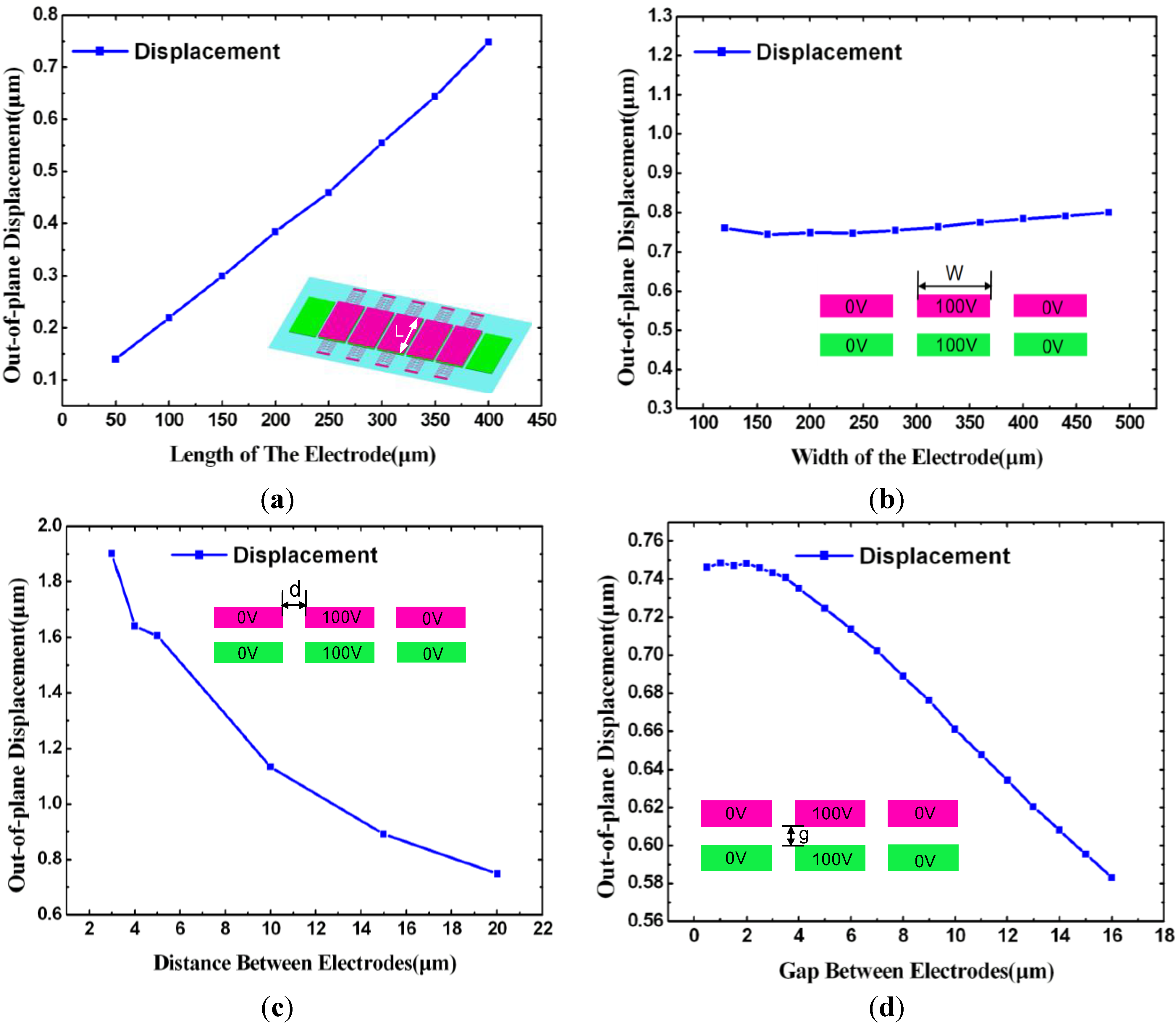
In this section, the influence of the length of the electrodes, the width of the electrodes, the gap between upper and lower electrodes and the distance between the two electrodes on the same layer to the displacement of the actuator in the repulsive mode are investigated. A commercial FEA software-Intellisuite [27] is utilized, and the applied voltage in simulation is maintained at 100 V. We assume that the upper and lower electrodes have the same length and width.
3.1. The Length of Electrodes
First, the influence of the length of electrodes (we assume that the upper and lower electrodes have the same length) is investigated. The length of the electrode is changed from 100 μm to 400 μm, in steps of 50 μm, and the simulation result is depicted in Figure 5a. In this figure, as the length of electrodes increases, the displacement goes up. The line is approximately linear, which means that the electrostatic repulsive force is directly proportional to the length of the electrodes.
3.2. The Width of Electrodes
The influence of electrode width (we assume that the upper and lower electrodes have the same width) on out-of-plane displacement is depicted in Figure 5b. As the electrode width varies from 120 μm to 480 μm, in steps of 40 μm, the out-of-plane displacement of the upper electrode shows no remarkable change, just varying from 0.74 μm to 0.79 μm. This means that the width of the electrode has no remarkable impact on the repulsive force or on the electrostatic repulsive forces on the left and right side of the electrodes.
Figure 5.
(a) Simulation results of displacement versus length of electrodes; (b) Simulation results of displacement versus width of electrodes; (c) Simulation results of displacement versus distance between electrodes; (d) Simulation results of displacement versus gap between upper and lower electrodes.

3.3. The Distance between Electrodes
After determining the influence of the dimensions of electrodes on displacement, the influence of distance between electrodes is studied. In simulation, the distance varies from 3 μm to 25 μm, and the schematic of the displacement versus distance between electrodes is shown in Figure 5c. This result shows that the larger the distance between electrodes, the smaller the displacement of the actuator, resulting from electrostatic repulsive force.
3.4. Gap between Upper and Lower Electrodes
The influence of the gap between upper and lower electrodes to the out-of-plane displacement is also investigated. As depicted in Figure 5d, the curve can be divided into two sections. From 0.5 μm to 3 μm, the out-of-plane displacement shows no remarkable change, and, as a result, in this section of the curve, the electrostatic repulsive force remains stable as the gap increases. In contrast, in the second section, as the gap increases from 3 μm to 16 μm, a consistent decrease of the out-of-plane actuator is observed. The larger the gap is, the smaller the electrostatic repulsive force will be.
4. Fabrication and Test
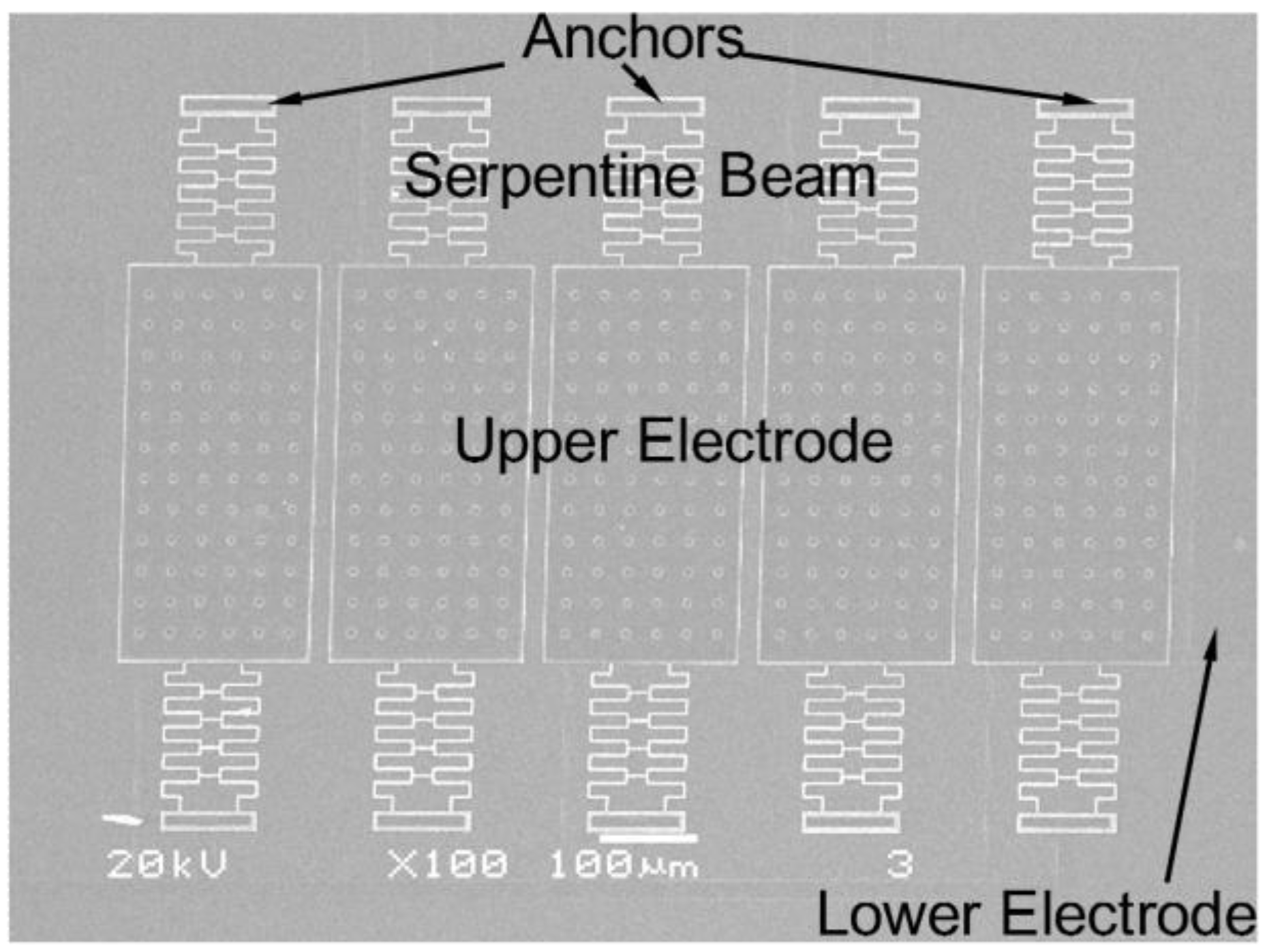
The bi-directional out-of-plane actuator is fabricated using a commercially available PolyMUMPs process [28], and Table 1 describes the dimensional parameters for fabrication. The fabrication flow is shown in Figure 6. First, 600 nm low-stress silicon nitride is deposited on an n-type (100) wafer with a diameter of 150 mm to form an electrical isolation layer (Figure 6a). Then 500 nm polysilicon film is deposited as Poly0 (Figure 6b). Afterward, Poly0 is patterned by photolithography and etched. Then 2 μm of phosphosilicate glass (PSG) is deposited as a sacrificial layer (Figure 6c). Then, Oxide1 is patterned by lithography and etched to form dimples (Figure 6d). The following step is to deposit a 2 μm polysilicon layer (Poly1) (Figure 6e), etched afterwards, to form a structural layer (Figure 6f). Finally the Oxide layer is sacrificed in a bath of 49% HF to release the structural layer (Figure 6g). The structure is dried by a supercritical CO2 drying technique. Figure 7 shows the Scanning Electron Microscopy (SEM) image of the structure.

| Description | Symbol | Parameter |
|---|---|---|
| Length of electrode | L | 400 |
| Width of electrode | w | 200 |
| Gap between electrodes | g | 2 |
| Distance between electrodes | d | 20 |
| Serpentine beam segment | A | 14 |
| Serpentine beam segment | B | 19 |
| Serpentine beam segment | C | 16 |
| Serpentine beam segment | D | 38 |
| Serpentine beam segment | E | 20 |
| Serpentine beam segment | F | 12 |
Figure 6.
Fabrication process of the bi-directional out-of-plane actuator.
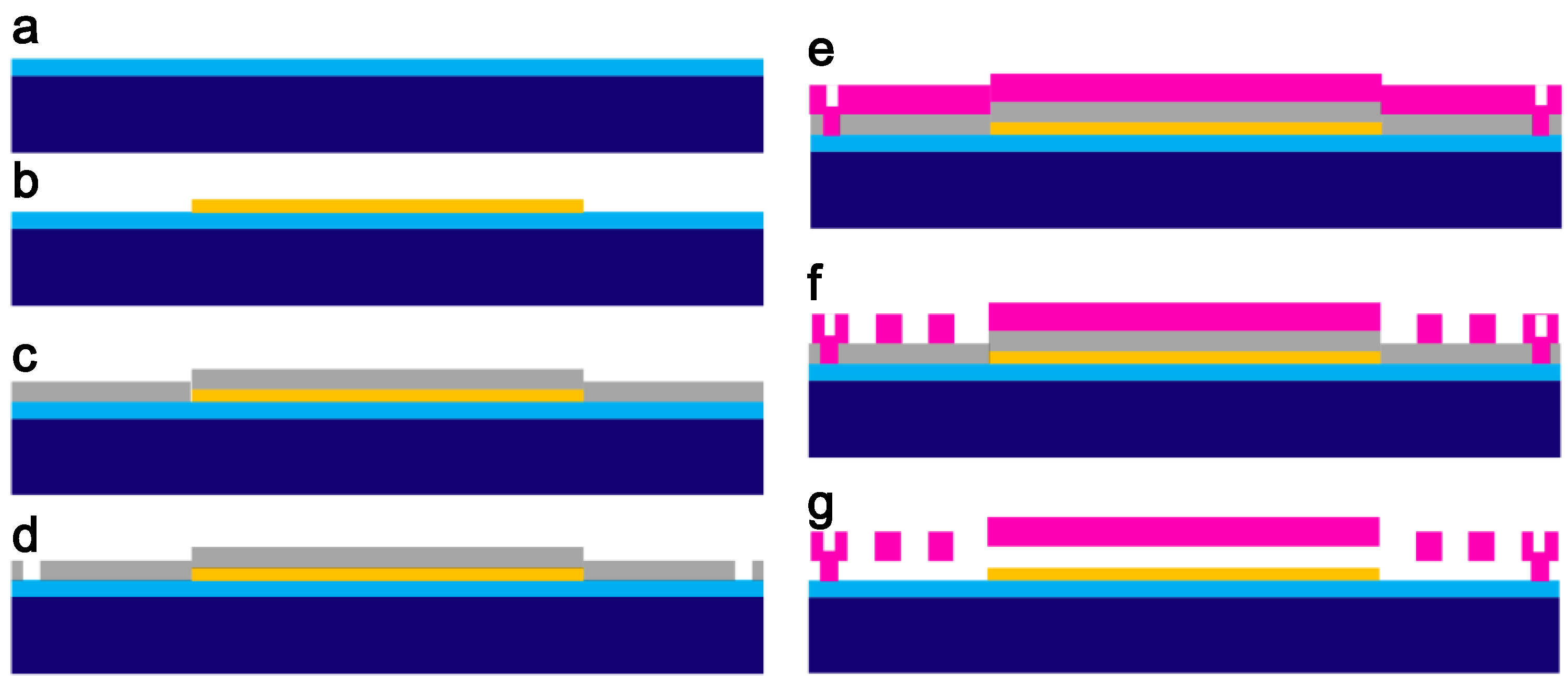
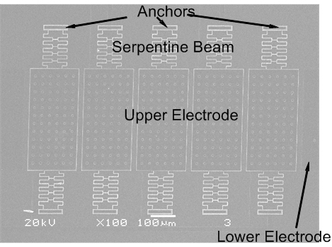
Figure 7.
SEM image of the prototype, electron gun voltage was set to be 20 kV, and amplification factor was 100×.
Figure 7.
SEM image of the prototype, electron gun voltage was set to be 20 kV, and amplification factor was 100×.
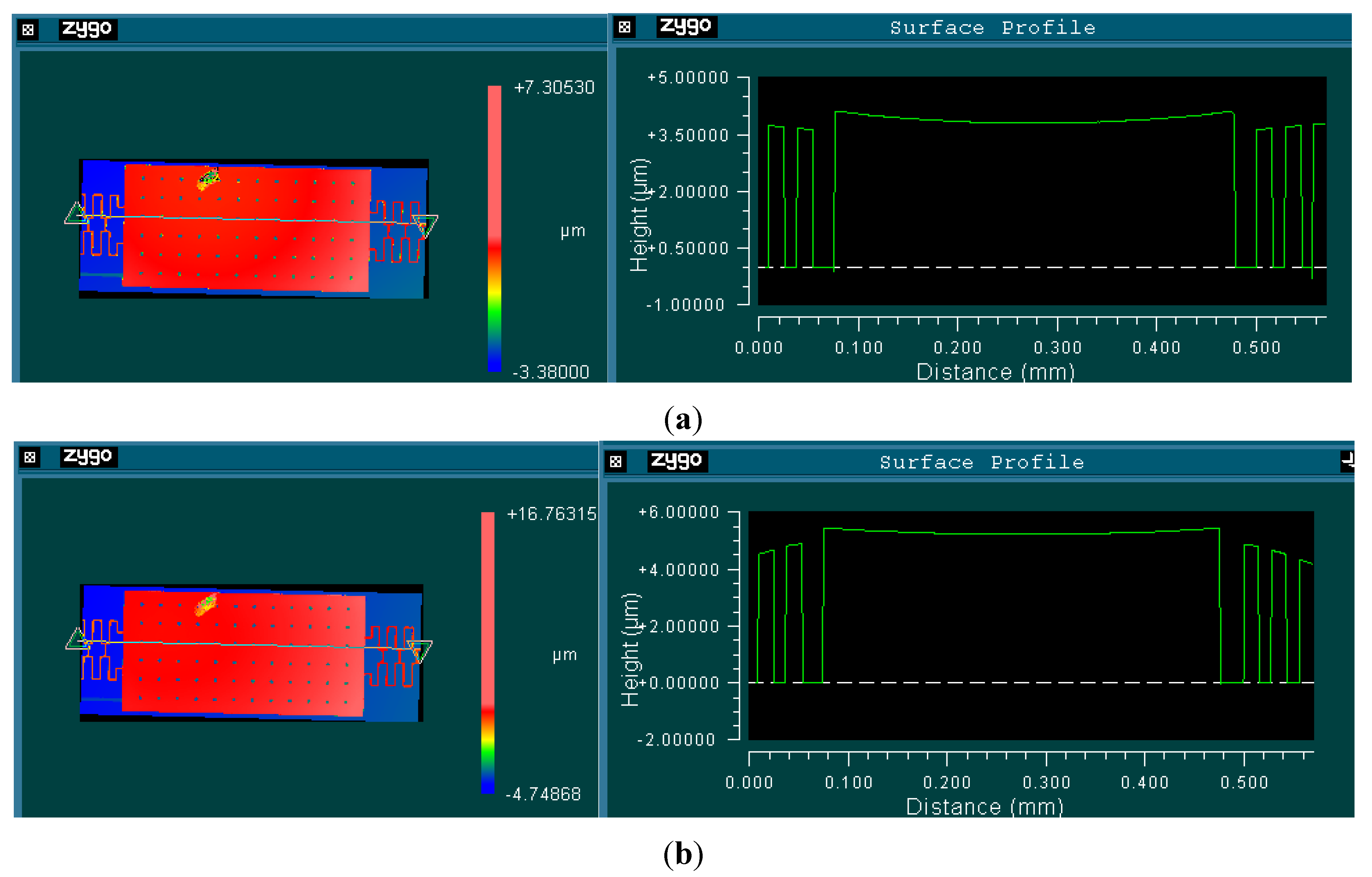
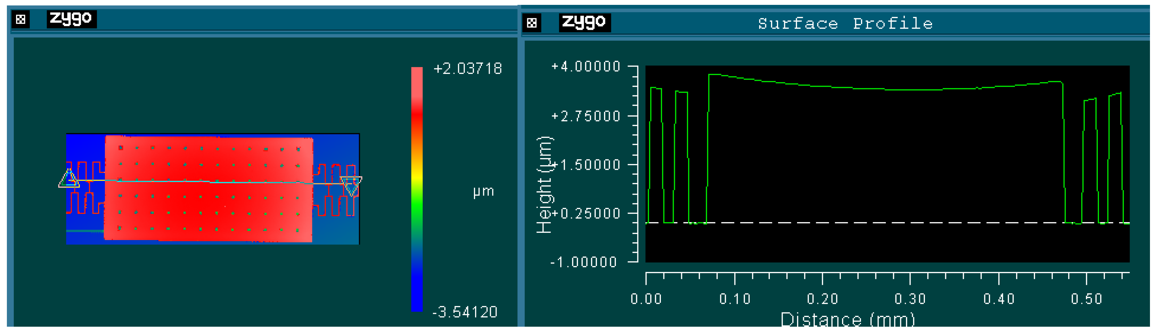
The static characteristics of the out-of-plane displacement versus voltage of the actuator are obtained using a white light interferometer, the Zygo Newview7300. First, the characteristics in the electrostatic repulsive mode are tested. The curve of the out-of-plane displacement versus voltage is illustrated in Figure 8. The surface profiles obtained when no voltage is applied and when a voltage of 130 V is applied are shown in Figure 9a,b, respectively. It is concluded that a displacement of 1.4 μm is obtained at the voltage of 130 V. When the voltage is higher than 130 V, electric break down occurs, and the device is broken due to short-circuit (high voltage creates a high electrical field, which breaks down the insulating air gap between adjacent electrodes with positive voltage and grounded. A high current flows through the air gap and between the adjacent electrodes (short-circuit), so the two interconnects for the adjacent layers will be burnt out (open circuit)).
Figure 8.
Test result of out-of-plane displacement versus voltage in the electrostatic repulsive mode.
Figure 8.
Test result of out-of-plane displacement versus voltage in the electrostatic repulsive mode.
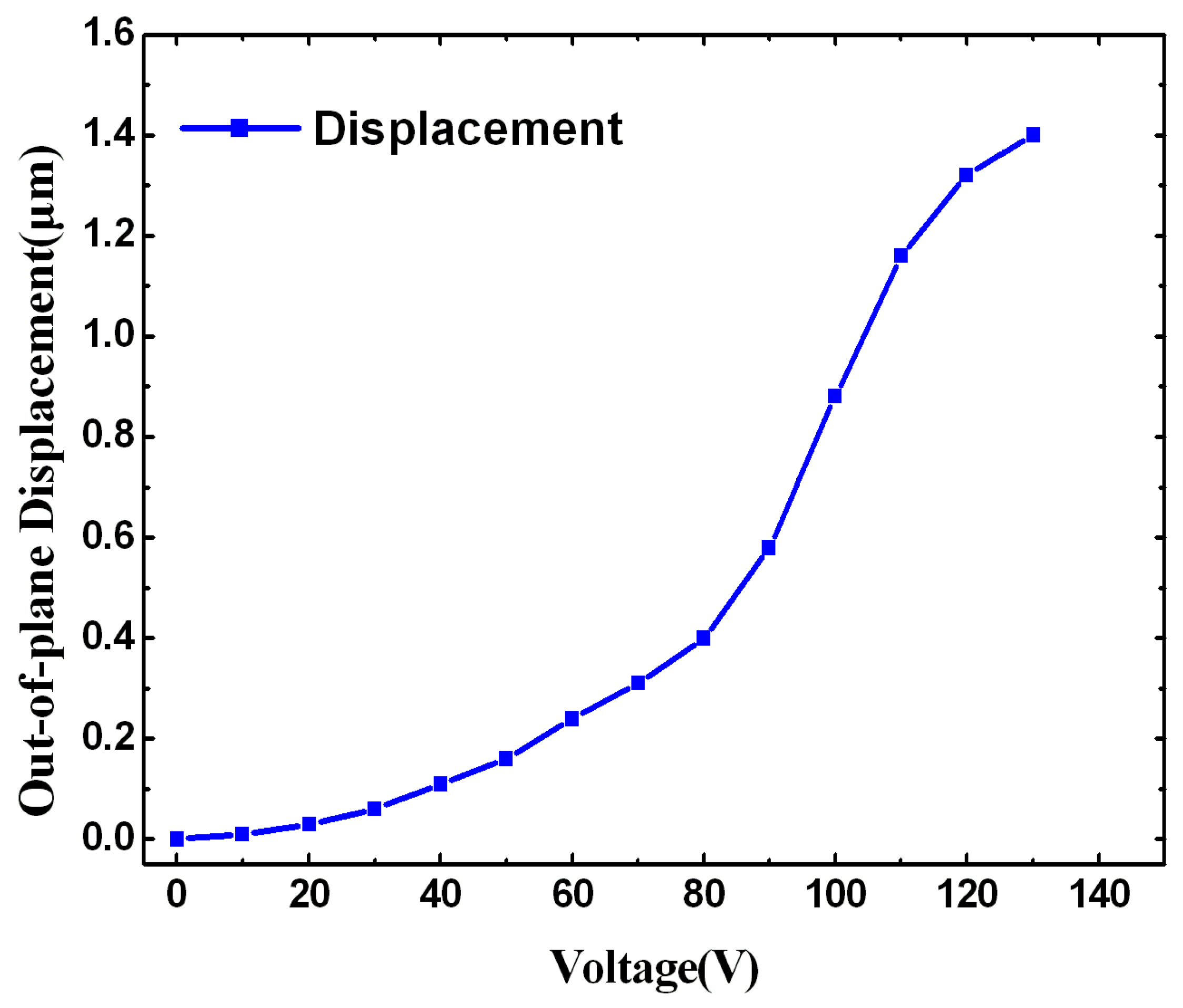
Figure 9.
(a) Surface profile of the actuator when no voltage is applied; (b) Surface profile of the actuator when a voltage of 130 V is applied in electrostatic repulsive mode.
Figure 9.
(a) Surface profile of the actuator when no voltage is applied; (b) Surface profile of the actuator when a voltage of 130 V is applied in electrostatic repulsive mode.

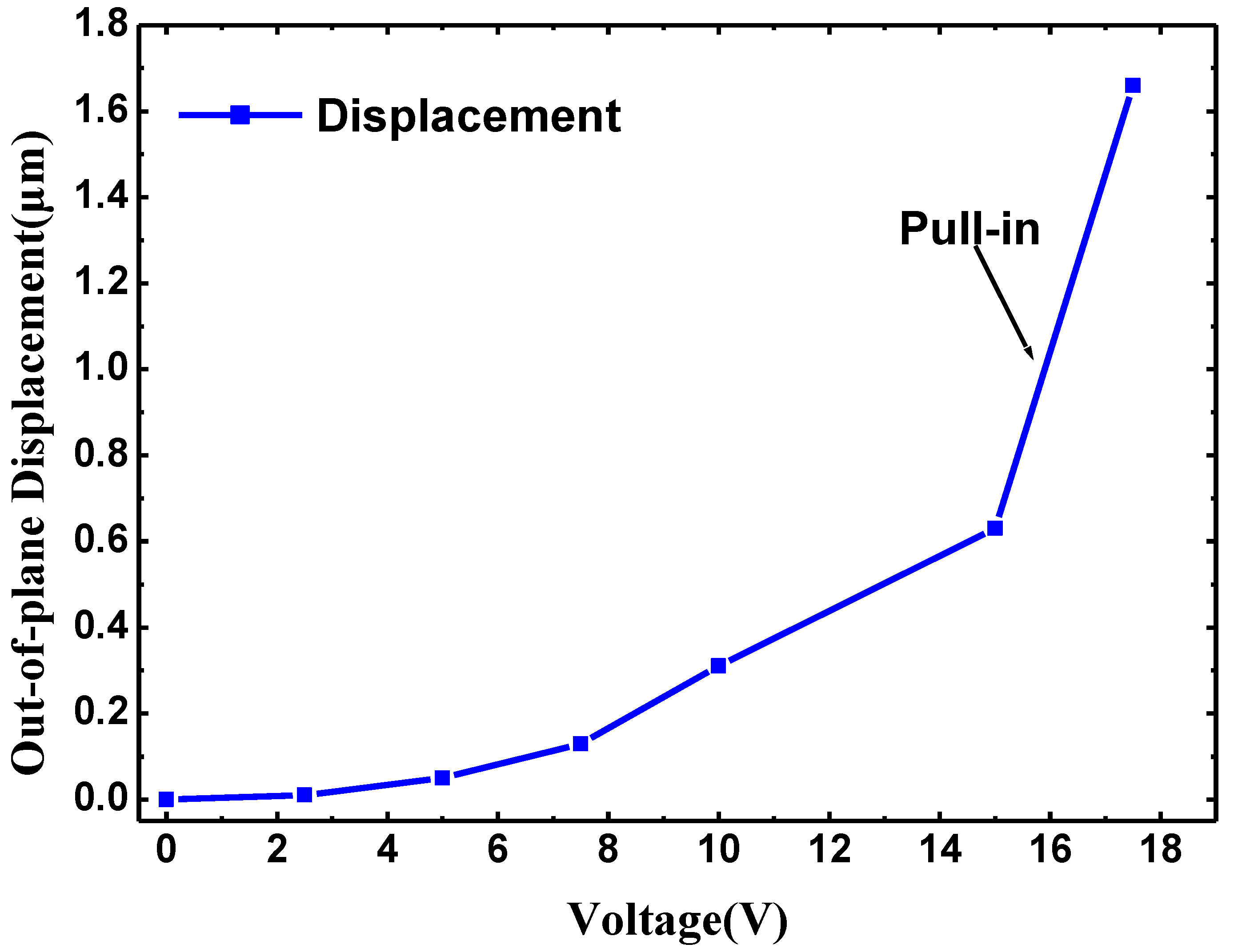
The curve of the out-of-plane displacement versus voltage in the electrostatic attractive mode is also tested, as depicted in Figure 10. The surface profile of the actuator at a voltage of 15 V is shown in Figure 11. When the applied voltage is higher than 15 V, the “pull-in” instability occurs. A displacement of 0.63 μm is achieved in this mode. As a result, the stroke of the bi-directional out-of-plane actuator can reach 2.03 μm, which is more than 3 fold that of the displacement of conventional out-of-plane actuator fabricated by the same fabrication process.
Figure 10.
Test results of out-of-plane displacement versus voltage in the electrostatic attractive mode.
Figure 10.
Test results of out-of-plane displacement versus voltage in the electrostatic attractive mode.

Figure 11.
Surface profile of the actuator when a voltage of 15 V is applied in electrostatic attractive mode.
Figure 11.
Surface profile of the actuator when a voltage of 15 V is applied in electrostatic attractive mode.

5. Conclusions
This paper describes a novel MEMS electrostatic out-of-plane actuator that works in two operation modes; the repulsive mode and the attractive mode. By combining the two modes, larger out-of-plane displacement can be obtained. This actuator also enjoys the virtue of lessening the “pull-in” instabilities by introducing the electrostatic repulsive mode. The influence of the length of electrodes and gap between electrodes on the out-of-plane displacement is studied using Finite Element Analysis. An out-of-plane actuator is fabricated by a commercially available surface polysilicon microfabrication process. Test results show that a total displacement of 2.03 μm is obtained in this actuator, the sum of 1.4 μm in the electrostatic repulsive mode and 0.63 μm in the electrostatic attractive mode.
Acknowledgments
This research is supported by the National Special Fund for the Development of Major Research Equipment and Instrument (Grant 2011YQ03012407) and National Natural Science Foundation of China-NSAF (Grant 11176033).
Conflicts of Interest
The authors declare no conflict of interest.
References
- Horenstein, M.N.; Pappas, S.; Fishov, A.; Bifano, T.G. Electrostatic micromirrors for subaperturing in an adaptive optics system. J. Electrostat. 2002, 54, 321–332. [Google Scholar] [CrossRef]
- Hah, D.; Huang, S.-Y.; Tsai, J.-C.; Toshiyoshi, H.; Wu, M.C. Low-voltage, large-scan angle mems analog micromirror arrays with hidden vertical comb-drive actuators. J. Microelectromech. Syst. 2004, 13, 279–289. [Google Scholar] [CrossRef]
- Stewart, J.B.; Bifano, T.G.; Cornelissen, S.; Bierden, P.; Levine, B.M.; Cook, T. Design and development of a 331-segment tip–tilt–piston mirror array for space-based adaptive optics. Sens. Actuators A Phys. 2007, 138, 230–238. [Google Scholar] [CrossRef]
- Carr, E.; Olivier, S.; Solgaard, O. Large-stroke self-aligned vertical comb drive actuators for adaptive optics applications. Proc. SPIE 2006, 6133. [Google Scholar] [CrossRef]
- Feng, Z.; Zhang, W.; Su, B.; Harsh, K.F.; Gupta, K.; Bright, V.; Lee, Y. Design and Modeling of RF MEMS Tunable Capacitors using Electro-thermal Actuators. In Proceedings of Microwave Symposium Digest, 1999 IEEE MTT-S International, Anaheim, CA, USA, 13–19 June 1999; pp. 1507–1510.
- Rebeiz, G.M.; Muldavin, J.B. RF MEMS switches and switch circuits. IEEE Microw. Mag. 2001, 2, 59–71. [Google Scholar] [CrossRef]
- Bakri-Kassem, M.; Mansour, R.R. Two movable-plate nitride-loaded MEMS variable capacitor. IEEE T. Microw. Theory 2004, 52, 831–837. [Google Scholar] [CrossRef]
- He, S.; Mrad, R.B. A Novel MEMS Tunable Capacitor. In Proceedings of the 2004 International Conference on MEMS, NANO and Smart Systems, Banff, Alberta, Canada, 25–27 August 2004; pp. 618–622.
- Ji, C.-H.; Choi, M.; Kim, S.-C.; Lee, S.-H.; Kim, S.-H.; Yee, Y.; Bu, J.-U. An electrostatic scanning micromirror with diaphragm mirror plate and diamond-shaped reinforcement frame. J. Micromech. Microeng. 2006, 16, 1033. [Google Scholar] [CrossRef]
- Cugat, O.; Basrour, S.; Divoux, C.; Mounaix, P.; Reyne, G. Deformable magnetic mirror for adaptive optics: Technological aspects. Sens. Actuators A Phys. 2001, 89, 1–9. [Google Scholar] [CrossRef]
- Xu, X.-H.; Li, B.-Q.; Feng, Y.; Chu, J.-R. Design, fabrication and characterization of a bulk-pzt-actuated MEMS deformable mirror. J. Micromech. Microeng. 2007, 17, 2439. [Google Scholar] [CrossRef]
- Atre, A. Analysis of out-of-plane thermal microactuators. J. Micromech. Microeng. 2006, 16, 205. [Google Scholar] [CrossRef]
- Hardy, J.W. Adaptive Optics for Astronomical Telescopes; Oxford University Press: Oxford, UK, 1998. [Google Scholar]
- Hu, F.; Yao, J.; Qiu, C.; Ren, H. A MEMS micromirror driven by electrostatic force. J. Electrost. 2010, 68, 237–242. [Google Scholar] [CrossRef]
- Cornelissen, S.; Bierden, P.; Bifano, T. A 4096 element continuous facesheet mems deformable mirror for high-contrast imaging. J. Micro/Nanolith. MEMS MOEMS 2009, 8. [Google Scholar] [CrossRef]
- Wu, X.-t.; Brown, R.A.; Mathews, S.; Farmer, K. Extending the Travel Range of Electrostatic Micro-Mirrors Using Insulator Coated Electrodes. In Proceedings of 2000 IEEE/LEOS International Conference on Optical MEMS, Sheraton Kauai, HI, USA, 21–24 August 2000; pp. 151–152.
- Helmbrecht, M.A.; He, M.; Juneau, T.; Hart, M.; Doble, N. Segmented MEMS deformable-mirror for wavefront correction. Proc. SPIE 2006, 6376. [Google Scholar] [CrossRef]
- Dagel, D.J.; Cowan, W.D.; Spahn, O.B.; Grossetete, G.D.; Griñe, A.J.; Shaw, M.J.; Resnick, P.J.; Jokiel, B., Jr. Large-stroke MEMS deformable mirrors for adaptive optics. J. Microelectromech. Syst. 2006, 15, 572–583. [Google Scholar] [CrossRef]
- Deladi, S.; Krijnen, G.; Elwenspoek, M. Parallel-beams/lever electrothermal out-of-plane actuator. Microsyst. Technol. 2004, 10, 393–399. [Google Scholar] [CrossRef]
- Tsai, J.-C.; Wu, M.C. Design, fabrication, and characterization of a high fill-factor, large scan-angle, two-axis scanner array driven by a leverage mechanism. J. Microelectromech. Syst. 2006, 15, 1209–1213. [Google Scholar] [CrossRef]
- Ren, H.; Tao, F.; Wang, W.; Yao, J. An out-of-plane electrostatic actuator based on the lever principle. J. Micromech. Microeng. 2011, 21, 045019. [Google Scholar] [CrossRef]
- Ren, H.; Ni, Z.G.; Chen, J.M.; Gong, A.L.; Yao, J. A micro spatial light modulator based on leverage principle. Key Eng. Mat. 2011, 483, 137–142. [Google Scholar] [CrossRef]
- Lee, K.B.; Cho, Y.-H. Laterally driven electrostatic repulsive-force microactuators using asymmetric field distribution. J. Microelectromech. Syst. 2001, 10, 128–136. [Google Scholar] [CrossRef]
- He, S.; Ben Mrad, R. Design, modeling, and demonstration of a MEMS repulsive-force out-of-plane electrostatic micro actuator. J. Microelectromech. Syst. 2008, 17, 532–547. [Google Scholar] [CrossRef]
- Yao, J.; Hu, F.; Cai, D.; Jiang, W. Design and analysis of repulsive electrostatic driven MEMS actuators. Proc. SPIE 2009, 7209. [Google Scholar] [CrossRef]
- Ren, H.; Hu, F; Qiu, C.; Yao, J. Design and analysis of a novel out-of-plane actuator. (in Chinese). J. Micronanoelectron. Technol. 2009, 46, 546–550. [Google Scholar]
- IntelliSense. Available online: http://www.intellisense.com (accessed on 1 November 2013).
- MUMPs. Available online: http://www.memscap.com/en_mumps.html (accessed on 1 November 2013).
© 2013 by the authors; licensee MDPI, Basel, Switzerland. This article is an open access article distributed under the terms and conditions of the Creative Commons Attribution license (http://creativecommons.org/licenses/by/3.0/).
Share and Cite
MDPI and ACS Style
Ren, H.; Wang, W.; Tao, F.; Yao, J. A Bi-Directional Out-of-Plane Actuator by Electrostatic Force. Micromachines 2013, 4, 431-443. https://doi.org/10.3390/mi4040431
AMA Style
Ren H, Wang W, Tao F, Yao J. A Bi-Directional Out-of-Plane Actuator by Electrostatic Force. Micromachines. 2013; 4(4):431-443. https://doi.org/10.3390/mi4040431
Chicago/Turabian StyleRen, Hao, Weimin Wang, Fenggang Tao, and Jun Yao. 2013. "A Bi-Directional Out-of-Plane Actuator by Electrostatic Force" Micromachines 4, no. 4: 431-443. https://doi.org/10.3390/mi4040431