Design Issues for Low Power Integrated Thermal Flow Sensors with Ultra-Wide Dynamic Range and Low Insertion Loss


Abstract
:
1. Introduction
2. Design Parameters and Optimization
2.1. Description of the Sensor Structure and Main Performance Parameters


- (a)Sensitivity, defined as S = dVout/dQ. The sensitivity depends generally on the input flow rate, although differential calorimeters exhibit a nearly linear behavior at small flow rates, where a constant sensitivity S(0) can be used. The sensitivity alone is not a real figure of merit, but it is a fundamental parameter for the design of the interface and, together with other parameters, contributes to the resolution and detection limit, defined below.
- (b)Resolution, defined as the minimum variation of the input flow that can be detected. The resolution is expressed in terms of the equivalent noise flow rate, Qnp−p = vnp−p/S, where vnp−p is the peak to peak amplitude of the total output noise voltage.
- (c)Offset flow rate, defined as QO = vO/S(0), where vO is the total offset voltage. The offset flow rate coincides with the reading of the flow sensor when the fluid velocity is zero.
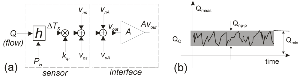
- (d)Detection limit Qmin, defined as the minimum (unsigned) flow value that can be reliably detected by the flow sensor. This parameter is particularly important for leakage sensors, which should be able to determine if very small flow rates are present. Figure 2(b) shows a sketched time diagram of the flow sensor readings in conditions of zero flow. If calibration of the offset is not performed, Q0 is an unknown quantity and we only have statistical information about it, i.e., we can presume that it falls between –Q0max and Q0max, where Q0max is the maximum offset for that kind of sensor. It is apparent that, in this case, if a reading is within –Q0max − Qnp−p/2 and Q0max + Qnp−p/2, it is not possible to determine whether a flow rate is present or Q = 0 and the measurement is simply the result of a possible combination of offset and noise. Therefore, in the case of no offset calibration, the detection limit is Qmin = QOmax + Qnp−p/2. Even if an offset calibration procedure is applied, a residual offset will still be present. The detection limit coincides with the theoretical limit Qnp−p/2 only if the residual offset is negligible with respect to noise.
- (e)Bandwidth, B, defined as the frequency range of the flow velocity in which the sensor sensitivity remains over nearly 70% of the value for constant flow. The sensor response time is inversely proportional to the bandwidth. Note that the intrinsic bandwidth, due to the sensor thermal masses and resistances, can be further reduced in the interface to limit the noise and improve resolution.
- (f)Full scale flow rate, Qmax. The response of thermal flow sensors tends to saturate at high flows, for the effect of several concomitant causes. As a result, the sensitivity progressively drops, degrading the resolution. The maximum value Qmax can be conventionally set at the point where the sensitivity drops below a given fraction of the initial S(0) value. Response saturation is mainly due to fluid-dynamics and forced convection mechanisms that can be studied only by means of simulations or experiments. In this work we will provide some indications based on tests performed on different sensor configurations.
- (g)Dynamic range, DR=Qmax/Qnp−p. The DR coincides with the number of distinct flow levels that can be distinguished by the flow sensor. This parameter is particularly important for flow sensors used to measure large flow rates with high resolution. High dynamic range flow sensors are required in flow control units designed to deliver precise fluid flows to reaction chambers (as in semiconductor processing equipments [9]) or ionic thrusters for fine handling of satellite attitude and orbital parameters [11]. The DR of traditional macroscopic flow sensors is typically lower than 102 while it may exceed 103 in MEMS flow sensors.
- (h)Insertion loss, ploss, defined as the pressure drop across the sensor flow channel, measured at Qmax.
- (i)Power consumption PH. This is an extremely important parameter for battery powered applications.
2.2. Lumped Element Model of the Transduction Principle

 (1)
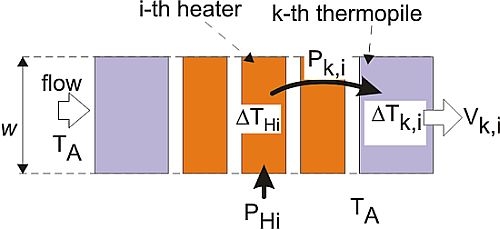
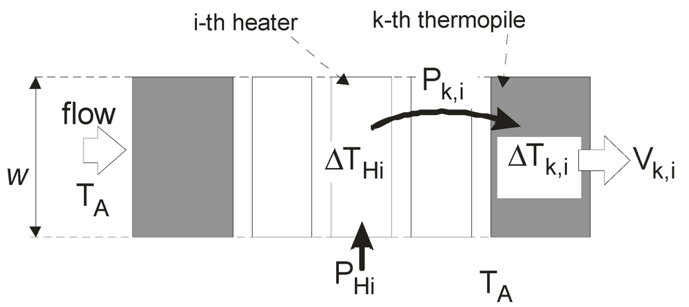
(1) is the total thermal resistance between the heater and the environment. The fraction of the power PHi, indicated with Pk,i that reaches hot junctions of the k-th thermopile can be expressed as:
 (2)
(2) (3)
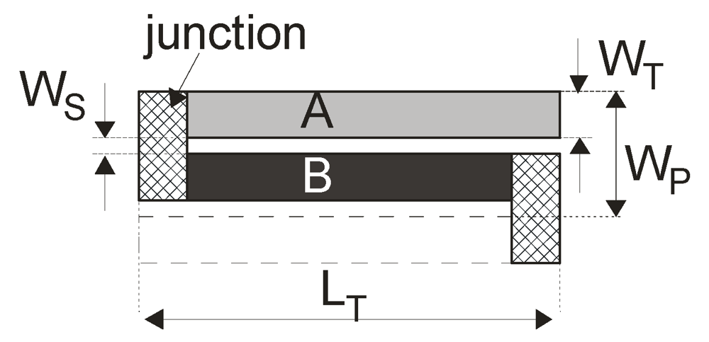
(3) is the thermal resistance between the thermopile hot junctions and the environment. For the structure of Figure 1(a) the thermal resistance is dominated by conduction through solid elements (cantilever), and is then given by:
 (4)
(4) (5)
(5) (6)
(6) (7)
(7) (8)
(8) (9)
(9) (10)
(10) (11)
(11) (12)
(12)2.3. Sensor Resolution
 (13)
(13)
 (14)
(14) (15)
(15) (16)
(16) (17)
(17) (18)
(18) (19)
(19)2.4. Offset Flow Rate
 (20)
(20) (21)
(21) (22)
(22) (23)
(23)2.5. Insertion Loss vs. Sensitivity
 (24)
(24) (25)
(25) (26)
(26) (27)
(27) (28)
(28)2.6. Design Considerations
 (29)
(29)- (1)The sensor width W should be set at the maximum allowed value, imposed by the fabrication process (etching times) and by the channel width WCH. Increasing WCH to make room for a further W increase is ineffective, since heff proportionally decreases through Equation (28).
- (2)The power PH should be set to the maximum value, which can be due either to a power consumption constraint or a reliability issue, the latter deriving from the maximum allowed heater temperature.
- (3)The effect of the thermopile number is rather weak, since it acts only on fNT, which varies in a narrow interval. From Equation (17) the optimum situation seems to be represented by NT = 1. Nevertheless, we will discover later that such a choice can adversely affect the amplifier design and should generally be avoided.
- (4)If the above operations are not sufficient to obtain the target resolution, parameter heff should be improved. The relevant equations are (5), (10) and (12). Improvement of the heater insulation (
![Micromachines 03 00295 i031]() ) is effective only if the power constraint does not derive from reliability issues, since, in this case, an increase of
) is effective only if the power constraint does not derive from reliability issues, since, in this case, an increase of ![Micromachines 03 00295 i031]() with the maximum allowed power applied would simply result in exceeding the maximum heater temperature. Improving the thermopile insulation by increasing LC produces significant heff improvements when LC < LS, so that LT is not proportionally affected. Furthermore, LC is often limited by the allowed etching times and mechanical robustness. Thermopile insulation can also be improved by reducing the cantilever thickness tc, as clearly shown by Equation (4). Using the post-processing approach, this parameter is determined by the dielectric thickness deriving from the original process. Thickness reduction can be achieved in the post-processing phase by selective etching steps. The minimum thickness value is fixed by structural issues and by the necessity to maintain a sufficient margin with respect to the thermopile conductors, in order to prevent them from being damaged by the etching process. The last parameter to be taken into account to improve the sensitivity is ∂gi,k/∂Q. Reducing the channel height (H) is strongly effective as shown by Equation (28). However, the concomitant pressure drop increase, deriving from Equation (26), should be carefully taken into account.
with the maximum allowed power applied would simply result in exceeding the maximum heater temperature. Improving the thermopile insulation by increasing LC produces significant heff improvements when LC < LS, so that LT is not proportionally affected. Furthermore, LC is often limited by the allowed etching times and mechanical robustness. Thermopile insulation can also be improved by reducing the cantilever thickness tc, as clearly shown by Equation (4). Using the post-processing approach, this parameter is determined by the dielectric thickness deriving from the original process. Thickness reduction can be achieved in the post-processing phase by selective etching steps. The minimum thickness value is fixed by structural issues and by the necessity to maintain a sufficient margin with respect to the thermopile conductors, in order to prevent them from being damaged by the etching process. The last parameter to be taken into account to improve the sensitivity is ∂gi,k/∂Q. Reducing the channel height (H) is strongly effective as shown by Equation (28). However, the concomitant pressure drop increase, deriving from Equation (26), should be carefully taken into account. - (5)If the previous steps are successful, then it is necessary to design an amplifier with an input noise just low enough not to significantly change the achieved resolution. To obtain that, the following condition should be met:
 (30)
(30)3. Experimental Results and Discussion
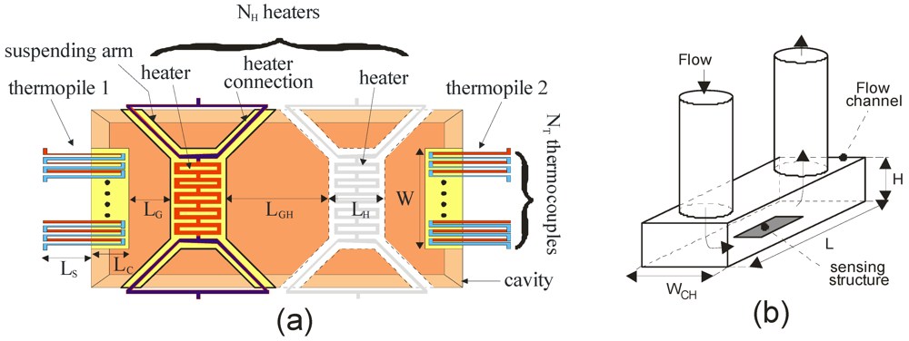
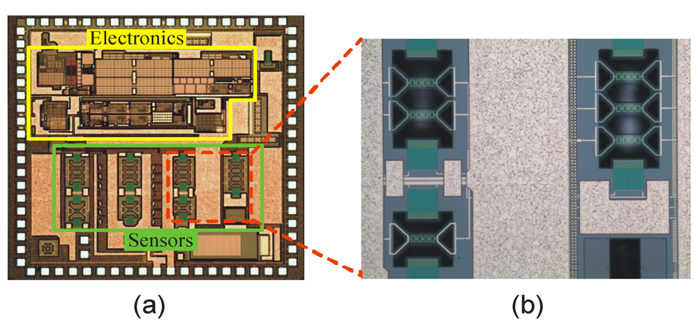
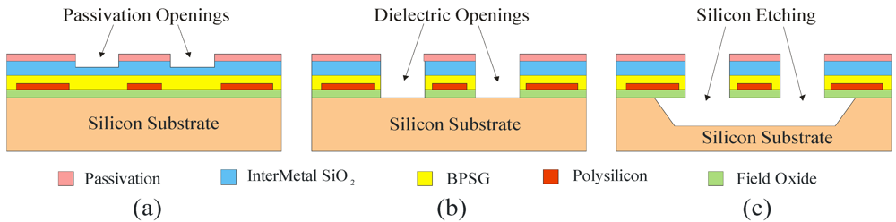
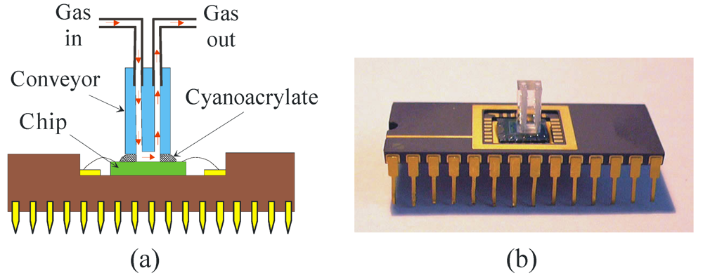
3.1. Test Chip Architecture and Technology


| NT | sAB | LC | LS | LH | LGH | W | L | WCH |
|---|---|---|---|---|---|---|---|---|
| 10 | 315 µV/K | 35 µm | 90 µm | 46 µm | 71 µm | 121 µm | 2 mm | 0.5 mm |


3.3. Measurements
| Sensor parameters | Sensor performance (PHi = PH/NH = 1.25 mW) | |||||||||
|---|---|---|---|---|---|---|---|---|---|---|
| NH | Heater | H | LG | S(0) | | ktpheff at Q = 0 | VK(0) | Qnp−p | Qmax | DR |
| connection | mm | µm | µV/sccm | K/mW | µV/sccm/mW | mV | sccm | sccm | ||
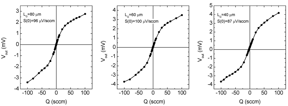
| 1 | Metal | 0.5 | 40 | 87 | 30.8 | 69.6 | 3.28 | 1.8 × 10⁻² | 30 | 1.7 × 10³ |
| 1 | Metal | 0.5 | 60 | 100 | 30.8 | 80 | 1.88 | 1.6 × 10⁻² | 21.5 | 1.3 × 10³ |
| 1 | Metal | 0.5 | 80 | 96 | 30.8 | 76.8 | 1.14 | 1.7 × 10⁻² | 20 | 1.2 × 10³ |
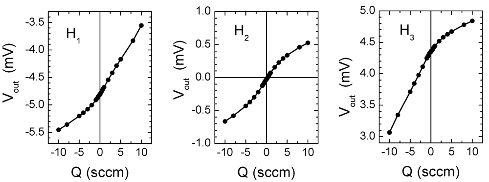
| 2 | Si-poly | 0.25 | 60 | 940 | 46.7 | 376 | 3.87 | 1.7 × 10⁻³ | 3.6 | 2.1 × 10³ |
| 2 | Si-poly | 0.5 | 60 | 313 | 46.7 | 125 | 3.61 | 5.1 × 10⁻³ | 12 | 2.3 × 10³ |
| 2 | Si-poly | 1 | 60 | 100 | 46.7 | 40 | 3.73 | 1.6 × 10⁻² | 42 | 2.6 × 10³ |
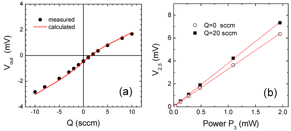
| 3 | Si-poly | 0.5 | 40 | 278 | 46.7 | 74 | 4.9 | 5.6 × 10⁻³ | 20 | 3.5 × 10³ |

4. Conclusions
Acknowledgments
References
- Schabmueller, C.G.J. Flow sensors. In MEMS Mechanical Sensors; Beeby, S., Ensell, G., Kraft, M., White, N., Eds.; Artech House: Norwood, MA, USA, 2004; pp. 213–256. [Google Scholar]
- Elwenspoek, M.; Wiegerink, R. Mechanical Microsensors, 1st ed; Springer-Verlag: Berlin, Germany, 2001; pp. 153–208. [Google Scholar]
- van Oudheusden, B.W. Silicon thermal flow sensors. Sens. Actuat. A: Phys. 1992, 30, 5–26. [Google Scholar] [CrossRef]
- Nguyen, N.T. Micromachined flow sensors–A review. Flow Meas. Instrum. 1997, 8, 7–16. [Google Scholar] [CrossRef]
- Baltes, H.; Paul, O.; Brand, O. Micromachined thermally based CMOS microsensors. Proc. IEEE 1998, 86, 1660–1678. [Google Scholar] [CrossRef]
- Wang, Y.-H.; Chen, C.-P.; Chang, C.-M.; Lin, C.-P.; Lin, C.-H.; Fu, L.-M.; Lee, C.-Y. MEMS-based gas flow sensors. Microfluid. Nanofluid. 2009, 6, 333–346. [Google Scholar] [CrossRef]
- de Bree, H.-E.; Jansen, H.V.; Lammerink, T.S.J.; Krijnen, G.J.M.; Elwenspoek, M. Bi-directional fast flow sensor with a large dynamic range. J. Micromech. Microeng. 1999, 9, 186–189. [Google Scholar] [CrossRef]
- Ashauer, M.; Glosch, H.; Hedrich, F.; Hey, N.; Sandmaier, H.; Lang, W. Thermal flow sensor for liquids and gases based on combinations of two principles. Sens. Actuat. A: Phys. 1999, 73, 7–13. [Google Scholar] [CrossRef]
- Henning, A.K.; Fitch, J.S.; Harris, J.M.; Dehan, E.B.; Cozad, B.A.; Christel, L.; Fathi, Y.; Hopkins, D.A., Jr.; Lilly, L.J.; McCulley, W.; et al. Microfluidic mems for semiconductor processing. IEEE Trans. Compon. Packag. Manuf. Technol. Part B 1998, 21, 329–337. [Google Scholar] [CrossRef]
- Fleming, W.J. New automotive sensors—A review. IEEE Sens. J. 2008, 8, 1900–1921. [Google Scholar] [CrossRef]
- Bejhed, J.; Eriksson, A.; Köhler, J.; Stenmark, L. The development of a micro machined xenon feed system. In Proceedings of the 40th AIAA/ASME/SAE/ASEE Joint Propulsion Conference, Exibit, FL, USA, 11–14 July 2004; pp. 1–8, AIAA 2004–3976.
- Bruschi, P.; Navarrini, D.; Piotto, M. A closed-loop mass flow controller based on static solid-state devices. J. Microelectromech. Syst. 2006, 15, 652–658. [Google Scholar] [CrossRef]
- Bruschi, P.; Dei, M.; Piotto, M. A low-power 2-D wind sensor based on integrated flow meters. IEEE Sens. J. 2009, 9, 1688–1696. [Google Scholar] [CrossRef]
- Lammerink, T.S.J.; Tas, N.R.; Elwenspoek, M.; Fluitman, J.H.J. Micro-liquid flow sensor. Sens. Actuat. A: Phys. 1993, 37–38, 45–50. [Google Scholar]
- Mayer, F.; Paul, O.; Baltes, H. Influence of design geometry and packaging on the response of thermal CMOS flow sensors. In Proceedings of the 8th International Conference on Solid-State Sensors and Actuators, and Eurosensors IX, Stockholm, Sweden, 25–29 June 1995; pp. 528–531.
- Mayer, F.; Salis, G.; Funk, J.; Paul, O.; Baltes, H. Scaling of thermal CMOS gas flow microsensors: Experiment and simulation. In Proceedings of the 9th Annual International Workshop on Micro Electro Mechanical Systems, MEMS '96, San Diego, CA, USA, 11–15 February 1996; pp. 116–121.
- Sabate, N.; Santander, J.; Fonseca, L.; Gracia, I.; Cane, C. Multi-range silicon micromachined flow sensor. Sens. Actuat. A 2004, 110, 282–288. [Google Scholar] [CrossRef]
- Roh, S.-C.; Choi, Y.-M.; Kim, S.-Y. Sensitivity enhancement of a silicon micromachined thermal flow sensor. Sens. Actuat. A 2006, 128, 1–6. [Google Scholar] [CrossRef]
- Kim, T.H.; Kim, D.-K.; Kim, S.J. Study of the sensitivity of a thermal flow sensor. Int. J. Heat Mass Transf. 2009, 52, 2140–2144. [Google Scholar] [CrossRef]
- Bruschi, P.; Ciomei, A.; Piotto, M. Design and analysis of integrated flow sensors by means of a two-dimensional finite element model. Sens. Actuat. A 2008, 142, 153–159. [Google Scholar] [CrossRef]
- Piotto, M.; Dei, M.; Butti, F.; Bruschi, P. A single chip, offset compensated multi-channel flow sensor with integrated readout interface. Procedia Eng. 2010, 5, 536–539. [Google Scholar] [CrossRef]
- Bruschi, P.; Diligenti, A.; Navarrini, D.; Piotto, M. A double heater integrated gas flow sensor with thermal feedback. Sens. Actuat. A 2005, 123–124, 210–215. [Google Scholar]
- Bruschi, P.; Dei, M.; Piotto, M. An offset compensation method with low residual drift for integrated thermal flow sensors. IEEE Sens. J. 2011, 11, 1162–1168. [Google Scholar] [CrossRef]
- Nguyen, N.T.; Dötzel, W. Asymmetrical locations of heaters and sensors relative to each other using heater arrays: A novel method for designing multi-range electrocaloric mass-flow sensors. Sens. Actuat. A 1997, 62, 506–512. [Google Scholar] [CrossRef]
- Moser, D.; Baltes, H. A high sensitivity CMOS gas flow sensor on a thin dielectric membrane. Sens. Actuat. A 1993, 37–38, 33–37. [Google Scholar]
- Enz, C.C.; Temes, G.C. Circuit techniques for reducing the effects of op-amp imperfections: Auotzeroing, correlated double sampling, and chopper stabilization. Proc. IEEE 1996, 84, 1584–1614. [Google Scholar]
- Steyaert, M.S.J.; Sansen, W.M.C.; Zhongyuan, C. A micropower low-noise monolithic instrumentation amplifier for medical purposes. IEEE J. Solid-State Circuits 1987, SC-22, 1163–1168. [Google Scholar]
- Bejan, A. Forced convection: Internal flows. In Heat Transfer Handbook; Bejan, A., Kraus, A.D., Eds.; Wiley: Hoboken, NJ, USA, 2003; pp. 395–438. [Google Scholar]
- Bruschi, P.; Piotto, M.; Bacci, N. Postprocessing, readout and packaging methods for integrated gas flow sensors. Microelectron. J. 2009, 40, 1300–1307. [Google Scholar] [CrossRef]
- Bruschi, P.; Nurra, V.; Piotto, M. A compact package for integrated silicon thermal gas flow meters. Microsyst. Technol. 2008, 14, 943–949. [Google Scholar] [CrossRef]
- Bruschi, P.; Dei, M.; Piotto, M. A single chip, double channel thermal flow meter. Microsyst. Technol. 2009, 15, 1179–1186. [Google Scholar] [CrossRef]
© 2012 by the authors; licensee MDPI, Basel, Switzerland. This article is an open-access article distributed under the terms and conditions of the Creative Commons Attribution license (http://creativecommons.org/licenses/by/3.0/).
Share and Cite
Bruschi, P.; Piotto, M. Design Issues for Low Power Integrated Thermal Flow Sensors with Ultra-Wide Dynamic Range and Low Insertion Loss. Micromachines 2012, 3, 295-314. https://doi.org/10.3390/mi3020295
Bruschi P, Piotto M. Design Issues for Low Power Integrated Thermal Flow Sensors with Ultra-Wide Dynamic Range and Low Insertion Loss. Micromachines. 2012; 3(2):295-314. https://doi.org/10.3390/mi3020295
Chicago/Turabian StyleBruschi, Paolo, and Massimo Piotto. 2012. "Design Issues for Low Power Integrated Thermal Flow Sensors with Ultra-Wide Dynamic Range and Low Insertion Loss" Micromachines 3, no. 2: 295-314. https://doi.org/10.3390/mi3020295