Multi-Port High Voltage Gain Modular Power Converter for Offshore Wind Farms
by
 , ,
, ,
Sen Song
1, 
Yihua Hu
1,
Kai Ni
1,*,
Joseph Yan
1,
Guipeng Chen
2,
Huiqing Wen
3 and
Xianming Ye
4 1
Department of Electrical Engineering and Electronics, The University of Liverpool, Liverpool L69 3BX, UK
2
College of Electrical Engineering, Zhejiang University, Hangzhou 310027, China
3
Department of Electrical Engineering and Electronics, Xi’an Jiaotong-Liverpool University, Suzhou 215123, China
4
Department of Electrical, Electronic and Computer Engineering, University of Pretoria, Pretoria 0084, South Africa
*
Author to whom correspondence should be addressed.
Sustainability 2018, 10(7), 2176; https://doi.org/10.3390/su10072176
Submission received: 30 May 2018
/
Revised: 22 June 2018
/
Accepted: 25 June 2018
/
Published: 26 June 2018
(This article belongs to the Special Issue Sustainable Development of Electrical Energy Storage Technologies in Energy Production)
Abstract
:In high voltage direct current (HVDC) power transmission of offshore wind power systems, DC/DC converters are applied to transfer power from wind generators to HVDC terminals, and they play a crucial role in providing a high voltage gain, high efficiency, and high fault tolerance. This paper introduces an innovative multi-port DC/DC converter with multiple modules connected in a scalable matrix configuration, presenting an ultra-high voltage step-up ratio and low voltage/current rating of components simultaneously. Additionally, thanks to the adoption of active clamping current-fed push–pull (CFPP) converters as sub-modules (SMs), soft-switching is obtained for all power switches, and the currents of series-connected CFPP converters are auto-balanced, which significantly reduce switching losses and control complexity. Furthermore, owing to the expandable matrix structure, the output voltage and power of a modular converter can be controlled by those of a single SM, or by adjusting the column and row numbers of the matrix. High control flexibility improves fault tolerance. Moreover, due to the flexible control, the proposed converter can transfer power directly from multiple ports to HVDC terminals without bus cable. In this paper, the design of the proposed converter is introduced, and its functions are illustrated by simulation results.
1. Introduction
The global number of offshore wind farms has increased in recent years [1,2]. In Europe, 560 new offshore wind turbines were built in 17 wind farms in 2017 with a total generation capacity of 3148 MW, which is about 20% of the total offshore generation capacity [3]. The power generated offshore is typically transmitted over an average distance of 41 km (in 2017) through submarine cables before reaching a connection point with the existing onshore grid [3]. For example, Hornsea wind farm is located around 40 km from the onshore station. Compared with high voltage alternating current (HVAC) transmission, high voltage direct current (HVDC) transmission is the preferred method to transfer power over a long distance (>40 km) in terms of the factors of economy and power efficiency [4,5]. When delivering the same amount of power, the purchase price for the bipolar HVDC cable is lower than that of two parallel 3-core HVAC ones [6]. Additionally, HVDC has a higher transmission efficiency than HVAC since no inductance-reactive power exists within DC transmission cables.
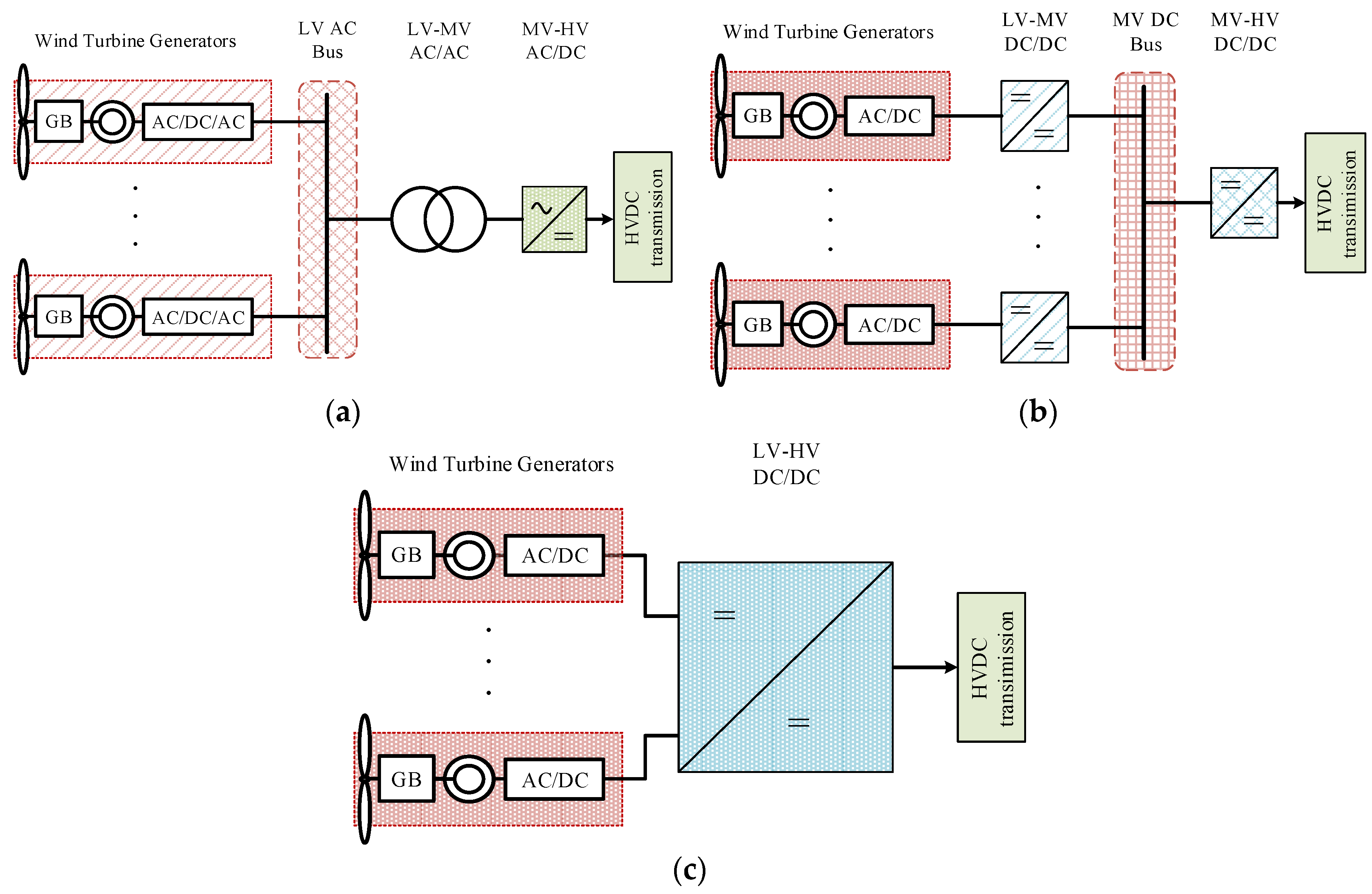
Figure 1 presents three HVDC configurations. The hybrid HVDC system illustrated in Figure 1a uses a medium voltage (MV)—high voltage (HV) AC/DC converter to obtain high voltage DC power. However, line-frequency (50/60 Hz) AC/AC transformers for low-voltage (LV)—MV conversion still occupy a significant portion of the substation space. In this topology, the transformer is replaced by a converter as shown in Figure 1b, which significantly reduces the system size and weight [7]. These two configurations use two-stage conversion to meet the voltage level of HVDC transmission. However, Reference [8] points out that the configuration of two DC/DC conversion stages has the highest power loss, which is around four times that of a one conversion stage configuration presented in Figure 1c taking into consideration the winding and core losses of transformers and the given datasheets of the semiconductors. The converter applied in Figure 1c not only provides a high voltage gain but also transfers power directly from multiple generators to HVDC terminals without bus cable. The converter design is a technical challenge for boosting LV directly to HV due to the conflict between the required high voltage level, e.g., ±800 kV [9] and the restricted voltage ratings of semiconductor components, e.g., 22 kV for SiC thyristors, and 15 kV for SiC transistors [10]. Fortunately, with the development of semiconductors and converter topologies, possible solutions are provided [11,12,13].
To address the challenges, DC converters with high voltage gains [14,15,16,17], modular multilevel converters (MMCs) [18,19,20,21,22] and multi-module converters [23,24,25] are studied extensively. Although dual-active bridge (DAB) converters [14,15] and resonant converters [16,17] can obtain high voltage step-up ratios, the voltage stress on their semiconductor components is high, which can be reduced by applying MMCs. By adding sub-modules (SMs), a high output voltage is achieved without increasing the voltage stress. However, the MMC topologies based on half-bridge (HB) or full-bridge (FB) [18,19] and resonant MMC [20] cannot provide electrical isolation. The isolated MMCs in References [21,22] are presented with DC/AC/DC configuration, where medium-frequency high turns-ratio transformers are employed, resulting in a vast volume. Although resonant MMCs [26] achieve galvanic isolation and a small volume of transformers at the same time, its conversion ratio only satisfies MV applications. Alternatively, transformers can be decentralized into multi-module converters, enabling the installation of high-frequency transformers, which reduces the sizes of transformers and reactive components. However, by adopting active-clamping flyback–forward converters as SMs, the currents of different SMs are unbalanced because of the non-ideal factors such as unequable leakage inductances of transformers, and only half of the power switches can achieve zero voltage switching (ZVS), resulting in high switching losses [23].
In this paper, based on the multi-modular converter in Reference [23], active-clamping current-fed push–pull (CFPP) converters are adopted to replace the flyback–forward SMs. The currents of modules in series-connection are auto-balanced, and all power switches can achieve soft-switching. Therefore, control complexity and switching loss are reduced. Furthermore, the matrix configuration brings about high control flexibility, which improves the fault tolerance capability. Additionally, thanks to the independent operation of each port, the converter can collect power from multiple sources without bus cable.
The paper is organized as follows: The basic cell and two interleaved working modes are analyzed in Section 1; the scalable topology design is discussed in Section 3; Section 4 depicts the fault tolerance strategies of the topology; simulation results are presented in Section 5 to demonstrate the effectiveness and efficiency of the converter, and finally, conclusions are drawn in Section 4.
2. Analysis of the Basic Cell and Working Strategies of Matrix Configuration
2.1. Operation of the Basic Cell
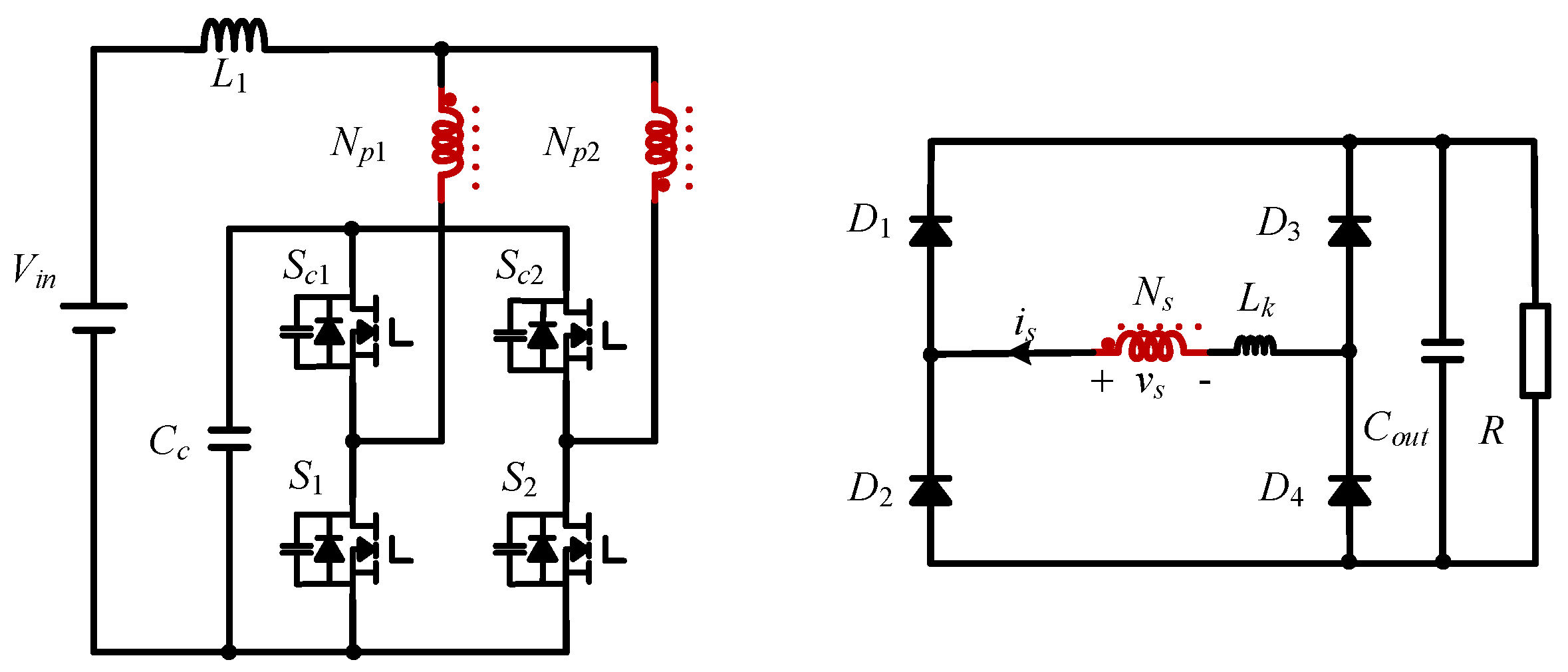
The basic cell topology based on CFPP converter shown in Figure 2 has similar operation principles and characteristics as the converter presented in Reference [27]. S1–S2 are the two main switches. Sc1–Sc2 are the two active clamping switches. Cc is the clamp capacitor. L1 is the input transistor. The tri-winding transformer has a turns ratio of Np1:Np2:Ns = 1:1:n and leakage inductance Lk at the secondary side. Furthermore, the secondary circuit consists of four rectifier diodes D1–D4, one output capacitor Cout and a load resistor R.
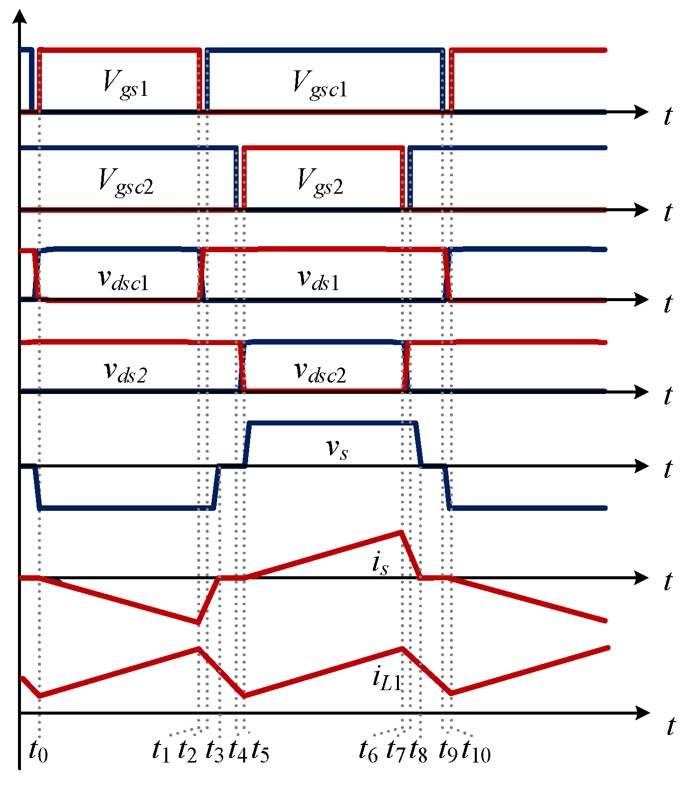
The key operating waveforms of CFPP cell are depicted in Figure 3. Vgs1–Vgs2 are the control signals for the two main switches S1–S2, which have the phase shift angle of 180°. Vgsc1–Vgsc2 are the control signals for the two clamp switches Sc1-Sc2. The control signals of the main switches and clamping switches are complementary. vds1–vds2 and vdsc1–vdsc2 are the drain-to-source voltages of the main switches and clamping switches respectively. iL1 is the current of input inductor L1. vs and is are the secondary voltage and current of the transformer respectively. The following assumptions are made to simplify the analysis.
- All switches and diodes are identical.
- The capacitance of clamp capacitor is large enough so that its voltage ripple can be ignored. Due to the symmetrical operation, a brief introduction of the operation during t0–t5 when D ≤ 0.5 is presented in this part.
Mode 1 (t0–t1): In this mode, the main switch S1 and the clamping switch Sc2 are on. The power is transferred to the output. The diodes D2 and D3 are forward biased, and the secondary current is decreases.
Mode 2 (t1–t2): At t1, the main switch S1 is turned off. The leakage inductances Lk resonate with the parasitic capacitances of S1 and Sc1. Then, the voltage of SC1 drops to zero at t2 to achieve ZVS turn-on. At the same time, capacitance CS1 is charged.
Mode 3 (t2–t3): At t2, the clamping switch SC1 is turned on with zero voltage. Because both the clamping switches SC1 and SC2 are on, the primary sides of the transformer are short-circuited. Then the power is transferred to the input inductor L1, and the secondary current is rises rapidly.
Mode 4 (t3–t4): At t3, the secondary current reaches zero. All four diodes are reverse biased. Additionally, the secondary voltage recovers to zero within a short time.
Mode 5 (t4–t5): At t4, the clamping switch SC2 is turned off. The leakage inductances Lk resonate with parasitic capacitances of S2 and SC2. The voltage across S2 drops to zero at t5 so that ZVS turn-on of S2 is obtained.
The operation in intervals (t0–t5) and (t5–t10) is symmetrical. The power is transferred to the output load R when one main switch and one clamping switch are on, and then the power flows from the input to inductor L1 when both clamping switches are on. All switches can obtain ZVS turn-on and the energy stored in Lk is recycled by the parasitic capacitances of clamping switches, which contributes to a higher conversion efficiency.
The voltage of clamp capacitor VCc can be obtained according to the flux balance of L1:
Additionally, with the turns ratio as 1:1:n, the output voltage of basic cell Vo,BC can be determined:
The voltage stress of all four power switches Vds can be obtained by:
2.2. Working Strategies of Matrix Configuration
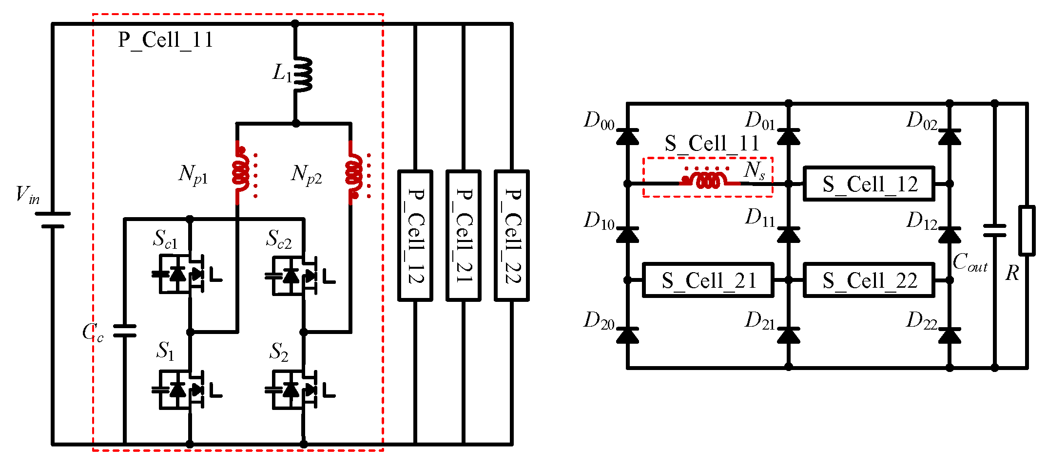
A fundamental 2 × 2 modular topology is presented in Figure 4. The primary circuits of power cells are parallel connected so that they have an equal secondary voltage value with the same duty cycle of main switches. The secondary side of each cell is connected with four rectifier diodes for power regulation.
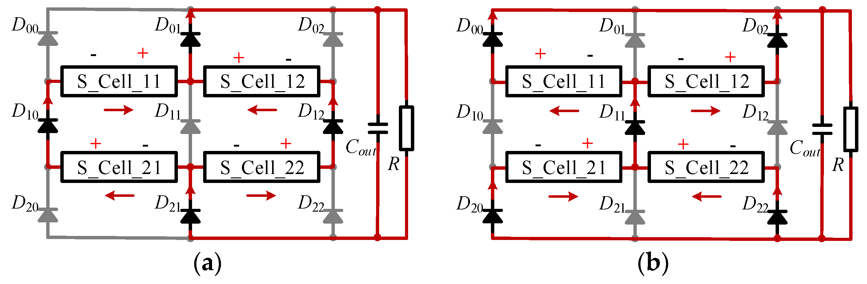
As illustrated in Figure 5a,b, adjacent cells have opposite polarities in column interleaved modes. For example, the polarity of cell 11 is opposite to those of cell 21 and 12. In this case, cells in the same column are connected in series, and the adjacent columns are in parallel connection. The voltage ratings of diodes in the first and last rows, D00–D02 and D20–D22, are equal to the voltage of power cells vs. While the voltage ratings of other diodes D10–D12 have twice the value of vs since they are connected with two cells. The current stresses of diodes in the first and last columns, D00–D20 and D02–D22 have the same value as the secondary current of one column. Diodes D01–D21 connect with two columns so that they have double the current stress of the others. Additionally, the sum of the average diode currents in all columns is equal to the output current. Therefore, in column interleaved modes, the voltage and current ratings of diodes in an expanded topology as shown in Figure 6 composed of s rows and p columns can be obtained:
where Io,BC is the average output current of a single basic cell; Vo,s×p and Io,s×p are the output voltage and current of s × p topology. In this case, all semiconductor components have low voltage and current ratings.
From Figure 5c,d, in series interleaved modes, all cells are series-connected. The cells in adjacent rows have the opposite polarities while the cells in the same row have the same polarity. Similar to Equation (4), diodes D10 and D12 have twice the voltage rating higher than that of diodes in the first and last rows because they connect with two rows. The currents of all operating diodes have the same value since they are in series-connection. Hence, the voltage and current ratings of diodes in series interleaved modes can be calculated as:
According to Equation (8), for series interleaved modes, the current rating of diodes is increased with the increase of output power. Besides which, the diodes D01–D21 are blocked, which benefits the fault tolerance operation to be described in Section 4.
3. Analysis of the Proposed Converter with Multi-Input Ports
3.1. Scalable Topology
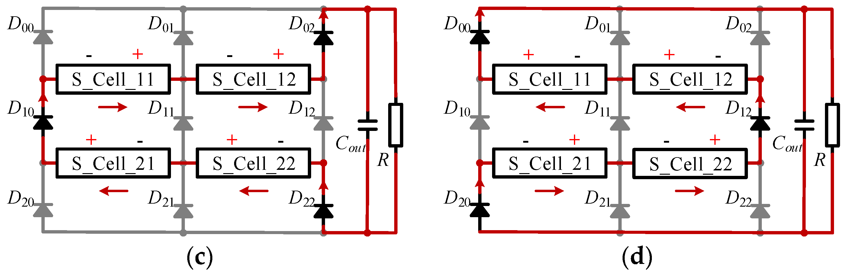
Thanks to modularity, multi-module converters can be easily expanded by increasing its row number and column number to attain a high voltage gain and the desired high power level. In the normal scenario, the proposed converter operates with column interleaved modes to keep a low voltage/current rating of components. Three wind-turbine-generators, WTGs 1–3, are connected to the proposed converter as illustrated in Figure 6a. Figure 6b shows the secondary circuits that are divided into three independent, Groups 1–3, by diodes D1-0p–D1-sp, D2-00–D1-s0 and D2-0p–D2-sp, D3-00–D3-s0 on the basis of input ports. The output power of each group consisting of the s × p expanded topology can be controlled individually, and the bus cable is eliminated. With the same input voltage and power of each port, the voltages and currents of all basic cells are identical.
The cells in the same column are in series-connection. Hence, every column has the same terminal voltage which is the sum of the voltages of cells in the same column. For a converter with multi-ports, output voltage Vout equals to the identical terminal voltage of columns and the output current Iout is the sum of secondary currents of all columns. Therefore, the row number s determines the output voltage, and the group number x with column number p determines the output power.
3.2. Current Balance with Column Interleaved Mode
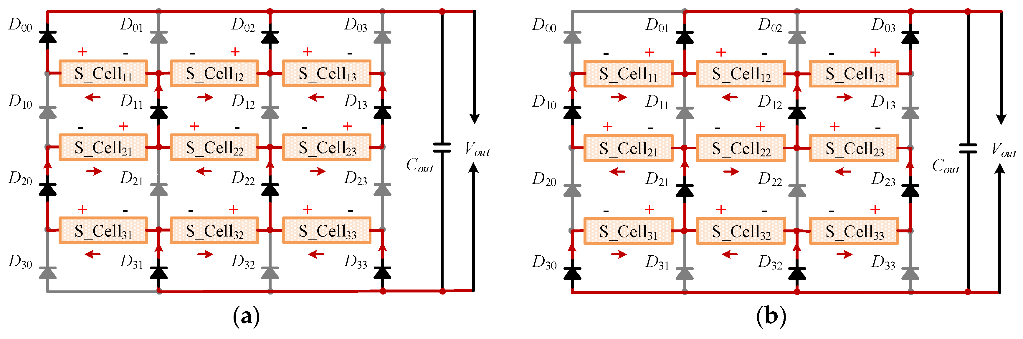
The control complexity is reduced by the auto-balanced currents of cells in the same column. According to the currents through diodes D10–D13 and D20–D23, as shown in Figure 7, the relationships among all cells can be obtained as:
where Io,BC+ is the average current of secondary circuit in the interval (t0–t5) and Io,BC− is that in the interval (t5–t10). According to the symmetrical operation of the basic cell between the two intervals, it can be derived that Io,BC+ = Io,BC−. Therefore, Equation (12) is obtained with Io,BC = Io,BC+ + Io,BC−.
According to Equation (12), the average currents for cells in the same column are auto-balanced. Therefore, as shown in Figure 8, only the control of output voltage and current sharing in different columns is employed to achieve the required output voltage and power in the s × p topology, where vo,ref is the desired output voltage and iL,i1–iL,ip are the currents collected from columns 1–p.
4. Fault Tolerance
4.1. Fault Tolerance for WTGs with Different Output Power
When disturbances occur, proper control strategies of WTGs and converters should be applied to ensure system protection and high power efficiency [28,29]. For the proposed converter, the output power of one group is determined not only by the column number of the secondary circuits but also, by the duty-cycles of main switches. According to Equation (8), the output power of one group is obtained as:
where m is the number of idle column in the corresponding group.
The variation of a duty-cycle will cause the change of currents through the cells in one column as:
Hence the output power is:
where imax is the maximum output current of power cells.
4.2. Fault Tolerance for Semiconductor Components
Semiconductor components are vulnerable components in a converter [30]. For offshore HVDC stations, faulty components take a long time for maintenance, resulting in high cost and loss [31].
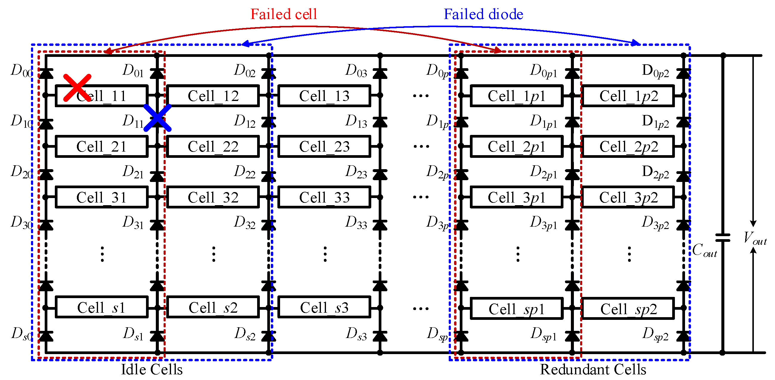
Figure 9 shows the fault tolerance operation derived by installing redundant power cells. To maintain normal operation, the column in a red dotted box containing the damaged Cell 11 is replaced by one redundant column that is in the other red dotted box. For the faulty diodes D00–Ds0, they require only one redundant column since they connect with one column. However, for other diodes, two redundant columns are demanded. For example, when diode D11 fails, the columns 1–2 in the blue dotted box are idle, and the redundant columns p1–p2 are applied.
The proposed topology can also obtain fault tolerant operation of diodes and power switches without redundancy. In Figure 10a,b, when diode D11 is short-circuited, the cells in rows 1–2 are inactive to block the faulty components, while the fault tolerance group still operates with the column interleaved strategy. Additionally, to maintain normal operation, the output voltages of the faulty group are controlled according to Equations (2) and (9) to ensure the output voltage is the same as that in the normal case. When diode D11 is open-circuited as illustrated in Figure 10c,d, the fault tolerant operation group consisting of two columns works under the series interleaved modes to block D11. Compared with the normal operation group, the number of cells in series connection in the faulty group is doubled. The voltages of cells in the fault group are adjusted as illustrated in Equation (15) to ensure they have the same terminal voltage.
Moreover, the fault tolerant operation of damaged cells without redundancy is similar to that when diodes are short-circuited. For instance, when cell 11 fails, cells 11-1p and 21-2p are idle so that the faulty one is blocked.
5. Simulation Results and Discussion
To illustrate the functionality of the proposed power converter, a simulation model consisting of 3 groups × 4 rows × 5 columns with 2 redundant columns is built by software PSIM, which is similar to the model shown in Figure 6. The cells in columns 1–3 are active, while those in columns 4–5 are inactive.
Table 1 presents the initial values for the simulation. It is noted that to verify the auto-balanced current characteristic, the leakage inductances of cells in column 1 are set as 70, 75, 80, 85 μH.
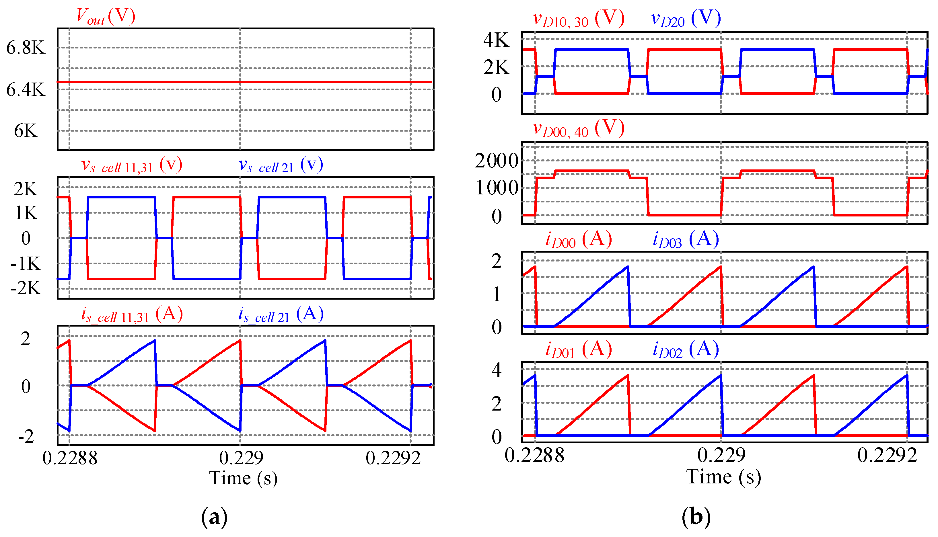
The steady-state waveforms of the converter with the same input power from WTGs are shown in Figure 11. All groups work under the column interleaved strategy, and the voltages of the adjacent cells in the same column have opposite polarities. Meanwhile, the currents of cells with diverse leakage inductances in column 1 are almost equal. The voltage stress of power switches is ¼ of the output voltage, and all diodes have the voltage and current stresses as low as ¼ or ½ of the output voltage and current, respectively.
For Figure 12, every group has different numbers of rows. Only one row operates in Group 1; in Group 2, there are two rows; Group 3 has four rows. The duty-cycle D of cells in each group is regulated to obtain the same terminal voltage, and the voltages of cells are shown in Figure 12 as: Vs_cell 1–11 = 2 × Vs_cell 2–11 = 4 × Vs_cell 3–11 = Vout.
The peak current values of different columns are almost equal so that the duty-cycle power transmission control presented in Equation (15) is verified.
Figure 13 shows the voltages of diodes in Group 1–2. The voltage of diodes in Group 3 has the same waveforms as those presented in Figure 10. It can be found that the voltage value is increased as the number of idle rows increases.
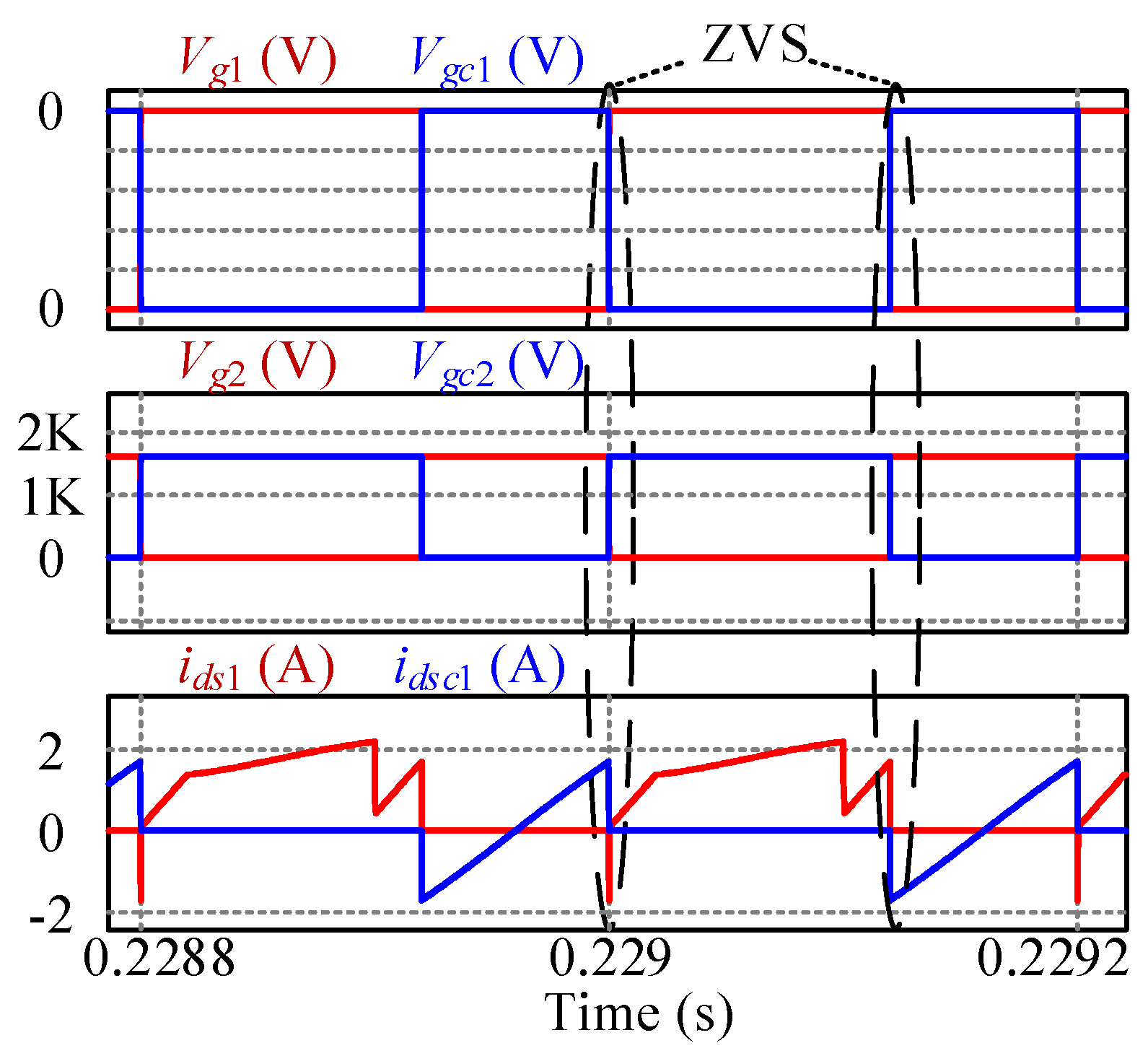
As illustrated in Figure 14, before turning on switches S1 or SC1, the drain-to-source current flows through the parasitic diode of the switch to achieve ZVS operation. Similarly, the switches S2 and SC2 can also obtain soft-switching. Therefore, the switching loss is significantly reduced.
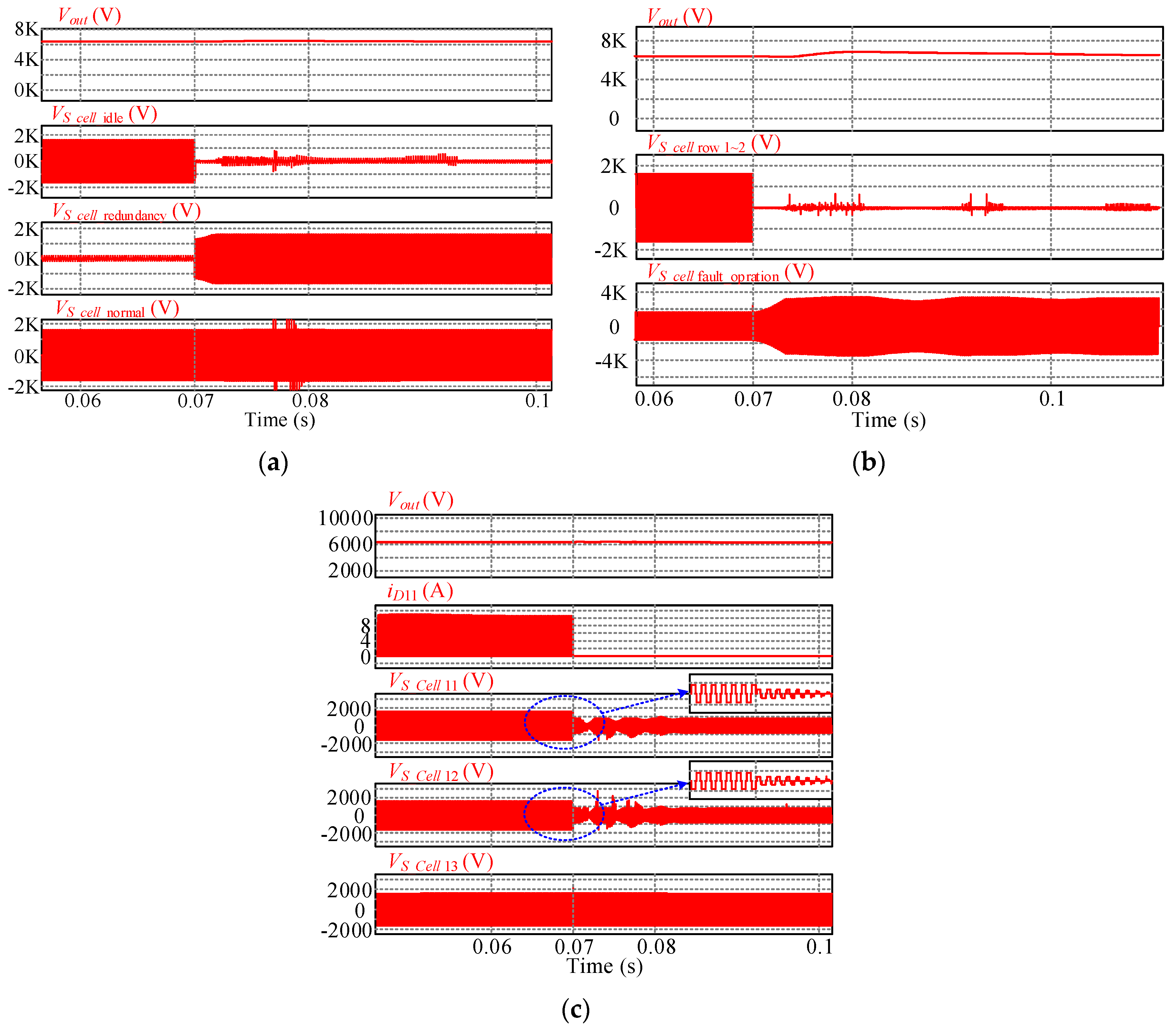
Figure 15a shows the fault tolerance operation with redundancy. At 0.07 s, fault cells 1–2 are idle, and the redundant columns 4–5 start to work to guarantee normal operation. Figure 15b,c presents the fault tolerance without redundancy, where only columns 1–3 are active. In Figure 15b, when the diode D11 is short-circuited, the cells in rows 1–2 are blocked. The voltages of cells in row 3–4 are doubled to achieve the same terminal voltage. The diode D11 is open in Figure 15c. The faulty group consisting of columns 1–2 works in the series interleaved mode by changing the polarities of cells. Moreover, the voltages of cells in the faulty group are reduced to half of that in the normal operation group to obtain the same output voltage.
Where N is the number of SMs or power cells; n is the turns ratio of transformers. Table 2 shows a performance comparison among several literatures. Due to hard switching, References [21,23] have higher switching losses. Multi-module converters can achieve a higher voltage step-up ratio by increasing the power cells number and the voltage gain of power cells. For MMCs, fault tolerance is achieved by redundancy. However, the proposed converter has an improved fault tolerance capability which can maintain normal operation without redundancy. Therefore, to achieve the same performance, a multi-module converter with CFPP cells requires fewer components.
6. Conclusions
A multi-port high voltage gain modular DC/DC power converter applied in offshore wind farms is proposed in this paper. Thanks to the modularity, the high output voltage and power is achieved by adding power cells. With the independent operation of each port and high control flexibility, the converter can collect power from multi-sources without bus cable. Additionally, the CFPP cells reduce the switching losses and control complexity.
The performances of MMC with galvanic isolation, resonant MMC, multi-module converter with flyback–forwarding cells and CFPP cells are compared. The proposed model appears to be more efficient and reliable, including fewer switching losses, higher conversion ratio, fewer components, smaller volume, and higher reliability.
The simulation results verify the advantages of the proposed converter are the soft-switching of all power switches, flexible control, and improved fault tolerance operation.
Author Contributions
Conceptualization, Y.H. and G.C.; Formal analysis, S.S. and Y.H.; Investigation, S.S.; Methodology, S.S., Y.H. and G.C.; Software, S.S. and G.C.; Supervision, Y.H.; Validation, S.S.; Writing—original draft, S.S.; Writing—review and editing, K.N., J.Y., H.W. and X.Y.
Funding
This study is supported by the State Key Laboratory of Alternate Electrical Power System with Renewable Energy Sources under Grant LAPS17022.
Conflicts of Interest
The authors declare no conflict of interest.
References
- Zervos, A.; Kjaer, C. Pure Power. Wind Energy Scenarios up to 2030; The European Wind Energy Association (EWEA): Brussels, Belgium, 2006. [Google Scholar]
- Council, G.W.E. Global Wind Report 2016. Available online: http://files.gwec.net/files/GWR2016.pdf?ref=Website (accessed on 25 June 2018).
- Remy, T.; Mbistrova, A. Offshore Wind in Europe-Key trends and statistics 2017. Available online: https://windeurope.org/wp-content/uploads/files/about-wind/statistics/WindEurope-Annual-Offshore-Statistics-2017.pdf (accessed on 25 June 2018 ).
- Oni, O.E.; Davidson, I.E.; Mbangula, K.N. A review of LCC-HVDC and VSC-HVDC technologies and applications. In Proceedings of the 2016 IEEE 16th International Conference on Environment and Electrical Engineering (EEEIC), Florence, Italy, 7–10 July 2016. [Google Scholar]
- Oates, C. Modular multilevel converter design for VSC HVDC applications. IEEE J. Emerg. Sel. Top. Power Electron. 2015, 3, 505–515. [Google Scholar] [CrossRef]
- Van Eeckhout, B.; Van Hertem, D.; Reza, M.; Srivastava, K.; Belmans, R. Economic comparison of VSC HVDC and HVAC as transmission system for a 300 MW offshore wind farm. Eur. Trans. Electr. Power 2009, 20, 661–671. [Google Scholar] [CrossRef]
- Chen, W.; Huang, A.Q.; Li, C.; Wang, G.; Gu, W. Analysis and comparison of medium voltage high power DC/DC converters for offshore wind energy systems. IEEE Trans. Power Electron. 2013, 28, 2014–2023. [Google Scholar] [CrossRef]
- Meyer, C.; Hoing, M.; Peterson, A.; De Doncker, R.W. Control and design of DC grids for offshore wind farms. IEEE Trans. Ind. Appl. 2007, 43, 1475–1482. [Google Scholar] [CrossRef]
- Wang, X.; Cao, C.; Zhou, Z. Experiment on fractional frequency transmission system. IEEE Trans. Power Syst. 2006, 21, 372–377. [Google Scholar]
- Vechalapu, K.; Bhattacharya, S.; Van Brunt, E.; Ryu, S.-H.; Grider, D.; Palmour, J.W. Comparative evaluation of 15-kv sic mosfet and 15-kv sic igbt for medium-voltage converter under the same dv/dt conditions. IEEE J. Emerg. Sel. Top. Power Electron. 2017, 5, 469–489. [Google Scholar] [CrossRef]
- Nami, A.; Liang, J.; Dijkhuizen, F.; Demetriades, G.D. Modular Multilevel Converters for HVDC Applications: Review on Converter Cells and Functionalities. IEEE Trans. Power Electron. 2015, 30, 18–36. [Google Scholar] [CrossRef]
- Ghat, M.B.; Shukla, A. A New H-Bridge Hybrid Modular Converter (HBHMC) for HVDC Application: Operating Modes, Control, and Voltage Balancing. IEEE Trans. Power Electron. 2018, 33, 6537–6554. [Google Scholar] [CrossRef]
- Gowaid, I.; Adam, G.; Massoud, A.M.; Ahmed, S.; Williams, B. Hybrid and Modular Multilevel Converter Designs for Isolated HVDC–DC Converters. IEEE J. Emerg. Sel. Top. Power Electron. 2018, 6, 188–202. [Google Scholar] [CrossRef]
- Soltau, N.; Stagge, H.; De Doncker, R.W.; Apeldoorn, O. Development and demonstration of a medium-voltage high-power dc-dc converter for dc distribution systems. In Proceedings of the 2014 IEEE 5th International Symposium on Power Electronics for Distributed Generation Systems (PEDG), Galway, Ireland, 24–27 July 2014. [Google Scholar]
- Engel, S.P.; Soltau, N.; Stagge, H.; De Doncker, R.W. Dynamic and balanced control of three-phase high-power dual-active bridge DC–DC converters in DC-grid applications. IEEE Trans. Power Electron. 2013, 28, 1880–1889. [Google Scholar] [CrossRef]
- Chen, W.; Wu, X.; Yao, L.; Jiang, W.; Hu, R. A step-up resonant converter for grid-connected renewable energy sources. IEEE Trans. Power Electron. 2015, 30, 3017–3029. [Google Scholar] [CrossRef]
- Meyer, C.; De Doncker, R.W. Design of a three-phase series resonant converter for offshore DC grids. In Proceedings of the 42nd IAS Annual Meeting. Conference Record of the 2007 IEEE on Industry Applications Conference, New Orleans, LA, USA, 23–27 September 2007. [Google Scholar]
- Kish, G.J.; Ranjram, M.; Lehn, P.W. A modular multilevel DC/DC converter with fault blocking capability for HVDC interconnects. IEEE Trans. Power Electron. 2015, 30, 148–162. [Google Scholar] [CrossRef]
- Martinez-Rodrigo, F.; Ramirez, D.; Rey-Boue, A.B.; de Pablo, S.; Herrero-de Lucas, L.C. Modular Multilevel Converters: Control and Applications. Energies 2017, 10, 1709. [Google Scholar] [CrossRef]
- Zhang, X.; Xiang, X.; Green, T.C.; Yang, X. Operation and Performance of Resonant Modular Multilevel Converter with Flexible Step Ratio. IEEE Trans. Ind. Electron. 2017, 64, 6276–6286. [Google Scholar] [CrossRef]
- Kenzelmann, S.; Rufer, A.; Dujic, D.; Canales, F.; De Novaes, Y.R. Isolated DC/DC structure based on modular multilevel converter. IEEE Trans. Power Electron. 2015, 30, 89–98. [Google Scholar] [CrossRef]
- Gowaid, I.; Adam, G.; Massoud, A.M.; Ahmed, S.; Holliday, D.; Williams, B. Quasi two-level operation of modular multilevel converter for use in a high-power DC transformer with DC fault isolation capability. IEEE Trans. Power Electron. 2015, 30, 108–123. [Google Scholar] [CrossRef]
- Hu, Y.; Zeng, R.; Cao, W.; Zhang, J.; Finney, S.J. Design of a Modular, High Step-Up Ratio DC–DC Converter for HVDC Applications Integrating Offshore Wind Power. IEEE Trans. Ind. Electron. 2016, 63, 2190–2202. [Google Scholar] [CrossRef] [Green Version]
- Chen, G.; Deng, Y.; He, X.; Hu, Y.; Jiang, L. Analysis of high voltage gain DC-DC converter with active-clamping current-fed push-pull cells for HVDC-connected offshore wind power. In Proceedings of the 42nd Annual Conference of the IEEE Industrial Electronics Society (IECON 2016), Florence, Italy, 23–26 October 2016. [Google Scholar]
- Mohammadpour, A.; Parsa, L.; Todorovic, M.H.; Lai, R.; Datta, R.; Garces, L. Series-input parallel-output modular-phase dc–dc converter with soft-switching and high-frequency isolation. IEEE Trans. Power Electron. 2016, 31, 111–119. [Google Scholar] [CrossRef]
- Xiang, X.; Zhang, X.; Chaffey, G.P.; Green, T.C. An Isolated Resonant Mode Modular Converter with Flexible Modulation and Variety of Configurations for MVDC Application. IEEE Trans. Power Deliv. 2017, 33, 508–519. [Google Scholar] [CrossRef]
- Nome, F.J.; Barbi, I. A ZVS clamping mode-current-fed push-pull DC-DC converter. In Proceedings of the IEEE International Symposium on Industrial Electronics (ISIE’98), Pretoria, South Africa, 7–10 July 1998. [Google Scholar]
- Duong, M.Q.; Leva, S.; Mussetta, M.; Le, K.H. A Comparative Study on Controllers for Improving Transient Stability of DFIG Wind Turbines during Large Disturbances. Energies 2018, 11, 480. [Google Scholar] [CrossRef]
- Wang, H.; Wang, Y.; Duan, G.; Hu, W.; Wang, W.; Chen, Z. An Improved Droop Control Method for Multi-Terminal VSC-HVDC Converter Stations. Energies 2017, 10, 843. [Google Scholar] [CrossRef]
- Yang, Z.; Chai, Y. A survey of fault diagnosis for onshore grid-connected converter in wind energy conversion systems. Renew. Sustain. Energy Rev. 2016, 66, 345–359. [Google Scholar] [CrossRef]
- Zhang, W.; Xu, D.; Enjeti, P.N.; Li, H.; Hawke, J.T.; Krishnamoorthy, H.S. Survey on fault-tolerant techniques for power electronic converters. IEEE Trans. Power Electron. 2014, 29, 6319–6331. [Google Scholar] [CrossRef]
- Zhang, X.; Green, T.C. The modular multilevel converter for high step-up ratio DC–DC conversion. IEEE Trans. Ind. Electron. 2015, 62, 4925–4936. [Google Scholar] [CrossRef]
Figure 1.
High voltage direct current (HVDC) configurations for wind power transmission: (a) DC-based connection with two-stage hybrid conversion; (b) DC-based connection with two-stage DC/DC conversion; (c) DC-based connection with the proposed modular converter.
Figure 1.
High voltage direct current (HVDC) configurations for wind power transmission: (a) DC-based connection with two-stage hybrid conversion; (b) DC-based connection with two-stage DC/DC conversion; (c) DC-based connection with the proposed modular converter.

Figure 2.
Topology of the basic cell based on active-clamping fed push–pull (CFPP) converter.

Figure 3.
Operating waveforms of the basic cell.

Figure 4.
2 × 2 topology of the isolated high voltage gain DC/DC converter with basic cells.

Figure 5.
2 × 2 topology with different interleaved strategies: (a) Column interleaved mode 1; (b) Column interleaved mode 2; (c) Series interleaved mode 1; (d) Series interleaved mode 2.
Figure 5.
2 × 2 topology with different interleaved strategies: (a) Column interleaved mode 1; (b) Column interleaved mode 2; (c) Series interleaved mode 1; (d) Series interleaved mode 2.


Figure 6.
Topology of the proposed converter with three input-ports: (a) primary circuits with three power sources; (b) secondary circuits collecting power and delivering it to load.
Figure 6.
Topology of the proposed converter with three input-ports: (a) primary circuits with three power sources; (b) secondary circuits collecting power and delivering it to load.

Figure 7.
Auto-balanced currents of cells in the same column with column interleaved working strategy: (a) Column interleaved working mode 1; (b) Column interleaved working mode 2.
Figure 7.
Auto-balanced currents of cells in the same column with column interleaved working strategy: (a) Column interleaved working mode 1; (b) Column interleaved working mode 2.

Figure 8.
Control scheme of the s × p topology.

Figure 9.
Fault tolerance with redundancy.

Figure 10.
Fault tolerance without redundancy: (a) Working mode 1 under diode short-circuit; (b) Working mode 2 under diode short-circuit; (c) Working mode 1 under diode open-circuit; (d) Working mode 2 under diode open-circuit.
Figure 10.
Fault tolerance without redundancy: (a) Working mode 1 under diode short-circuit; (b) Working mode 2 under diode short-circuit; (c) Working mode 1 under diode open-circuit; (d) Working mode 2 under diode open-circuit.


Figure 11.
Steady-state waveforms for cells and diode: (a) voltage/current of basic cells; (b) voltage/current of diodes.
Figure 11.
Steady-state waveforms for cells and diode: (a) voltage/current of basic cells; (b) voltage/current of diodes.

Figure 12.
Waveforms of cells when Groups 1–3 have different output power.

Figure 13.
Voltages of diodes in each Group when Groups 1–3 have different output power: (a) Voltages of diodes in Group 1; (b) Voltages of diodes in Group 2.
Figure 13.
Voltages of diodes in each Group when Groups 1–3 have different output power: (a) Voltages of diodes in Group 1; (b) Voltages of diodes in Group 2.

Figure 14.
Zero voltage switching (ZVS) of main switches and clamping switches.

Figure 15.
Fault tolerance operation: (a) With redundancy; (b) Without redundancy for D11 short-circuit; (c) Without redundancy for D11 open-circuit.
Figure 15.
Fault tolerance operation: (a) With redundancy; (b) Without redundancy for D11 short-circuit; (c) Without redundancy for D11 open-circuit.


Table 1.
Initial values of simulation.
| System Parameters | Values | Components | Values |
|---|---|---|---|
| Input Voltage | 650 V | Turns ratio 1:1:n | 1:1:2 |
| Output Voltage | 6400 V | Leakage inductance | 80 μH |
| Switching Frequency | 5 kHz | Input inductance | 5 mH |
| Output Power | 40 kW | Clamp capacitor | 20 μF |
© 2018 by the authors. Licensee MDPI, Basel, Switzerland. This article is an open access article distributed under the terms and conditions of the Creative Commons Attribution (CC BY) license (http://creativecommons.org/licenses/by/4.0/).
Share and Cite
MDPI and ACS Style
Song, S.; Hu, Y.; Ni, K.; Yan, J.; Chen, G.; Wen, H.; Ye, X. Multi-Port High Voltage Gain Modular Power Converter for Offshore Wind Farms. Sustainability 2018, 10, 2176. https://doi.org/10.3390/su10072176
AMA Style
Song S, Hu Y, Ni K, Yan J, Chen G, Wen H, Ye X. Multi-Port High Voltage Gain Modular Power Converter for Offshore Wind Farms. Sustainability. 2018; 10(7):2176. https://doi.org/10.3390/su10072176
Chicago/Turabian StyleSong, Sen, Yihua Hu, Kai Ni, Joseph Yan, Guipeng Chen, Huiqing Wen, and Xianming Ye. 2018. "Multi-Port High Voltage Gain Modular Power Converter for Offshore Wind Farms" Sustainability 10, no. 7: 2176. https://doi.org/10.3390/su10072176
Note that from the first issue of 2016, this journal uses article numbers instead of page numbers. See further details here.