Article

Annealing Effect on (FAPbI3)1−x(MAPbBr3)x Perovskite Films in Inverted-Type Perovskite Solar Cells

1
Department of Electro-Optical Engineering, National Taipei University of Technology, Chung-Hsiao E. Road, Taipei 10608, Taiwan
2
Research Center for New Generation Photovoltaics, National Central University, Taoyuan 32001, Taiwan
3
Material and Chemical Research Laboratories, Industrial Technology Research Institute, Hsinchu 31040, Taiwan
*
Author to whom correspondence should be addressed.
Materials 2016, 9(9), 747; https://doi.org/10.3390/ma9090747
Submission received: 27 June 2016 / Revised: 16 August 2016 / Accepted: 29 August 2016 / Published: 3 September 2016

Abstract

:
This study determines the effects of annealing treatment on the structure and the optical and electronic behaviors of the mixed (FAPbI3)1−x(MAPbBr3)x perovskite system. The experimental results reveal that (FAPbI3)1−x(MAPbBr3)x (x ~ 0.2) is an effective light-absorbing material for use in inverted planar perovskite solar cells owing to its large absorbance and tunable band gap. Therefore, good band-matching between the (FAPbI3)1−x(MAPbBr3)x and C60 in photovoltaic devices can be controlled by annealing at various temperatures. Accordingly, an inverted mixed perovskite solar cell with a record efficiency of 12.0% under AM1.5G irradiation is realized.

1. Introduction

Organic/inorganic hybrid perovskite materials of the form APbX3 (A = CH3NH3 or HC(NH2)2; X = I, Br or Cl) are attracting considerable interest owing to their potential for absorbing light in solar cells due to their broad spectral absorption, strong light harvesting, and long exciton diffusion length [1,2,3,4,5,6]. Perovskite solar cells (PSCs), which include perovskite materials as active absorption layers, have yielded good device performance with the highest power conversion efficiencies (PCEs) that have risen from approximately η = 3% efficiencies [7] to almost 20.2% [8]. Additionally, perovskite thin films of the form MAPbI3 can be prepared by the vapor-assisted solution method [9], the sequential deposition process [10,11,12], the one-step spin-coating method [13] and the two-step sequential method [14]; the corresponding processes are fast, simple, and low-cost. PSCs have been developed with two types of device architecture—conventional [10,11,12,13,14] and inverted [15]. Recently, Jeon et al. [16] reported on the compositional engineering of high-performance PSCs. They used mixed CH3NH3PbBr3 (MAPbBr3) and HC(NH2)2PbI3 (FAPbI3) in a solvent as a precursor to deposit (FAPbI3)x(MAPbBr3)1−x perovskite films on mesoporous TiO2 to form conventional PSCs. However, to the best of our knowledge, no detailed study of the mixing of FAPbI3 and MAPbBr3 perovskite in inverted PSCs has been published.
This work reports solution-process (FAPbI3)1−x(MAPbBr3)x perovskites (that are formed using a mixed solution of HC(NH2)2PbI3 (FAPbI3) and CH3NH3PbBr3 (MAPbBr3)) for use in PSCs with an inverted architecture. The (FAPbI3)1−x(MAPbBr3)x perovskites are formed by a one-step spin-coating process on PEDOT:PSS-coated ITO substrates. The optical, structural, and surface properties of the (FAPbI3)1−x(MAPbBr3)x perovskite films are investigated as functions of the thermal annealing temperature; the relationship between the performance of the PSC and the properties of the perovskite films is discussed.

2. Methods

In this study, a PEDOT:PSS film using a Trition X-100 (volume ratio PEDOT:PSS:Trition X-100 = 150:1) surfactant was spin-coated on a pre-cleaned ITO substrate at 5000 rpm for 30 s. After spin coating, the film was annealed at 140 °C for 10 min. The perovskite layer was deposited using the solvent-engineering technique [13] using a mixing solvent (in which the volume ratio of dimethyl sulfoxide (DMSO) to γ-butyrolactone (GBL) was 1:1). Then 0.96 mmol of FAPbI3 and 0.24 of mmol MAPbBr3 (i.e., 165 mg of FAI, 27 mg of MAB, 443 mg of PbI2 and 88 mg of PbBr2) were dissolved in the mixing solvent (1 mL) as a (FAPbI3)0.8(MAPbBr3)0.2 precursor solution. The perovskite precursor solution was coated onto the PEDOT:PSS/ITO substrate in two consecutive spin-coating steps at 1000 rpm and 5000 rpm for 10 s and 20 s, respectively. At 5000 rpm, the wet spinning film was quenched by dropping 50 μL of anhydrous toluene onto it. After spin coating, the film was annealed at 100 °C for 10 min. Subsequently, C60, Bathocuproine (BCP), and a silver (Ag) electrode were deposited to thicknesses of 50, 5 and 100 nm, respectively, using a thermal evaporator. The sample was covered with a shadow mask to define an active area of 0.5 cm × 0.2 cm during C60/BCP/Ag deposition. Figure 1a schematically depicts the complete structure.

Material and Device Measurement

The crystalline microstructures of the films were determined using a PANalytical X’Pert Pro DY2840 X-ray diffractometer with Cu-Kα radiation (PANalytical, Naerum, Denmark) (λ = 0.1541 nm). A field-emission scanning electron microscope (GeminiSEM, ZEISS, Oberkochen, Germany) was used to observe the surface morphology of the cells. Photoluminescence (PL) and absorption spectra were measured using a fluorescence spectrophotometer (Hitachi F-7000) (Hitachi High-Technologies Co., Tokyo, Japan) and a UV/VIS/NIR spectrophotometer (Hitachi U-4100 spectrometers) (Hitachi High-Technologies Co., Tokyo, Japan), respectively. Moreover, the current density-voltage (J-V) characteristics were measured using a Keithley 2420 programmable source meter (Keithley, Cleveland, OH, USA) under irradiation by a 1000 W xenon lamp. The scan rate is 0.1 V/s. Finally, the irradiation power density on the surface of the each sample was calibrated as 1000 W/m2.

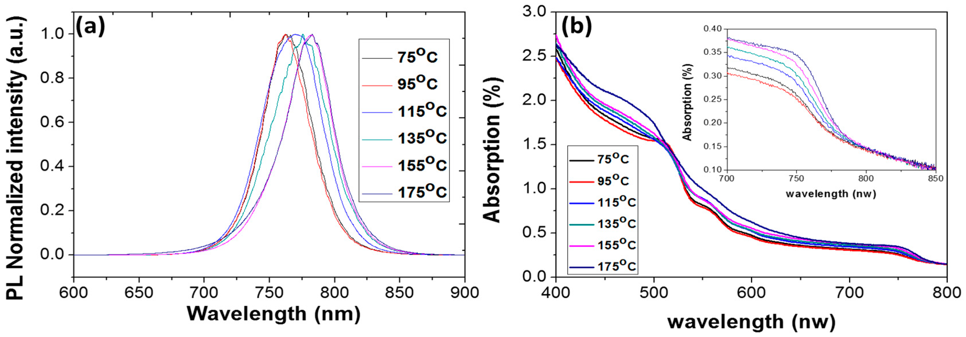
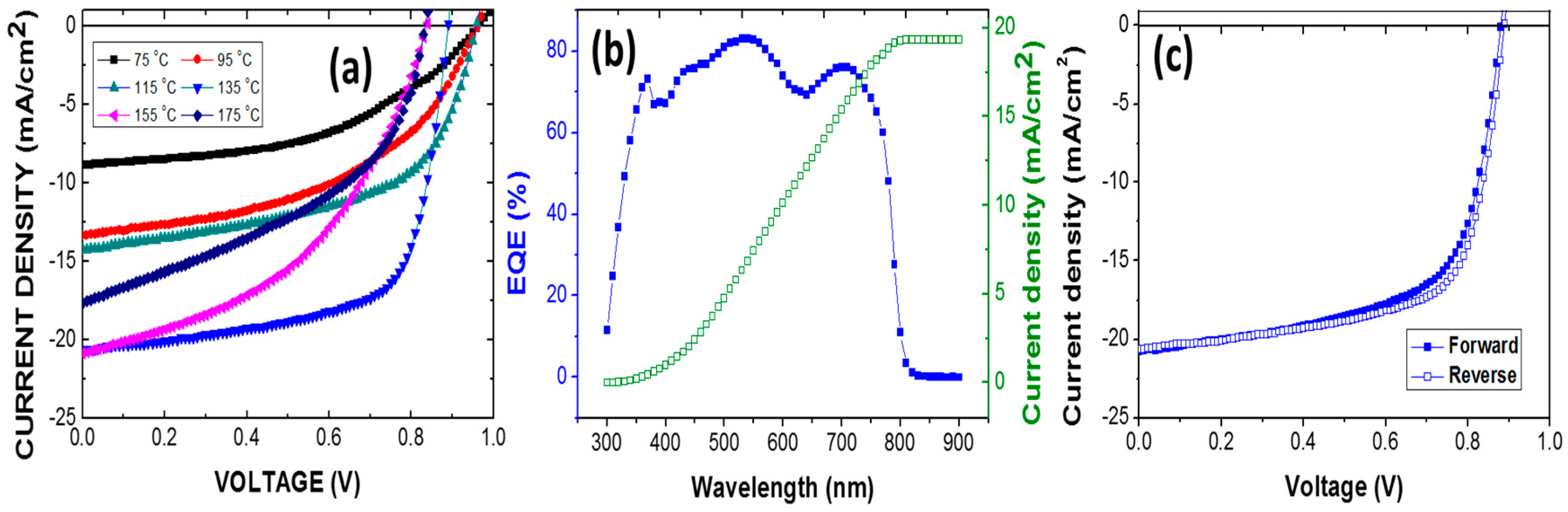
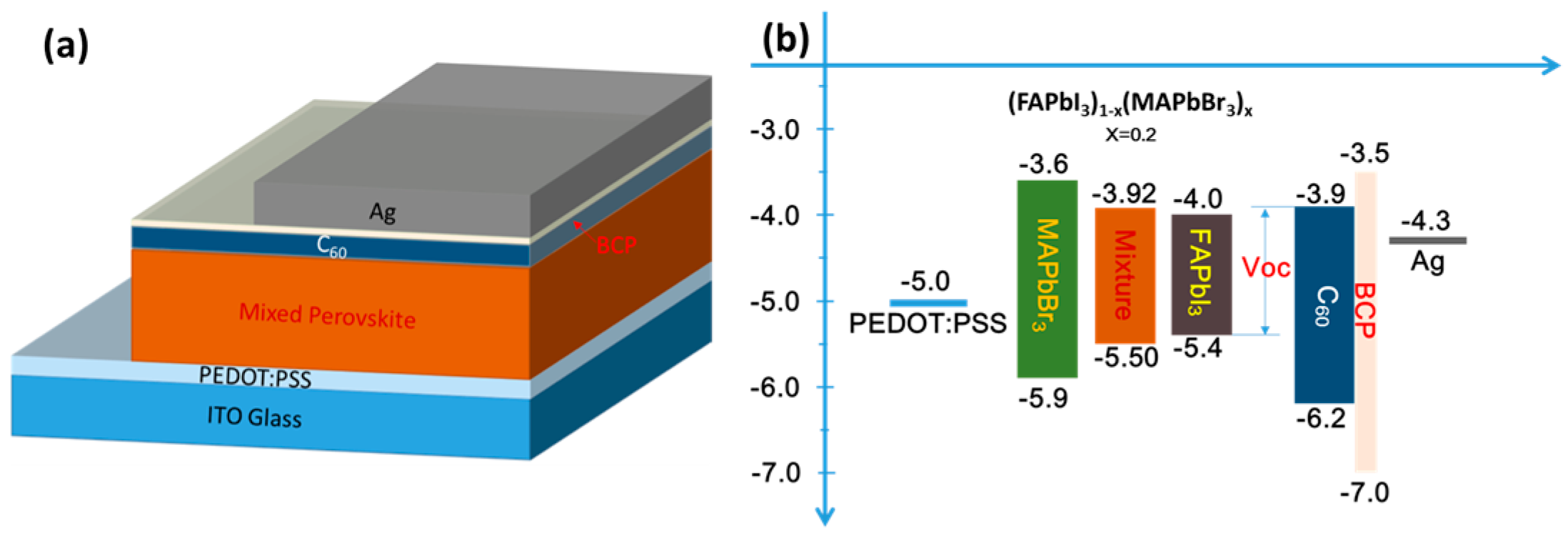
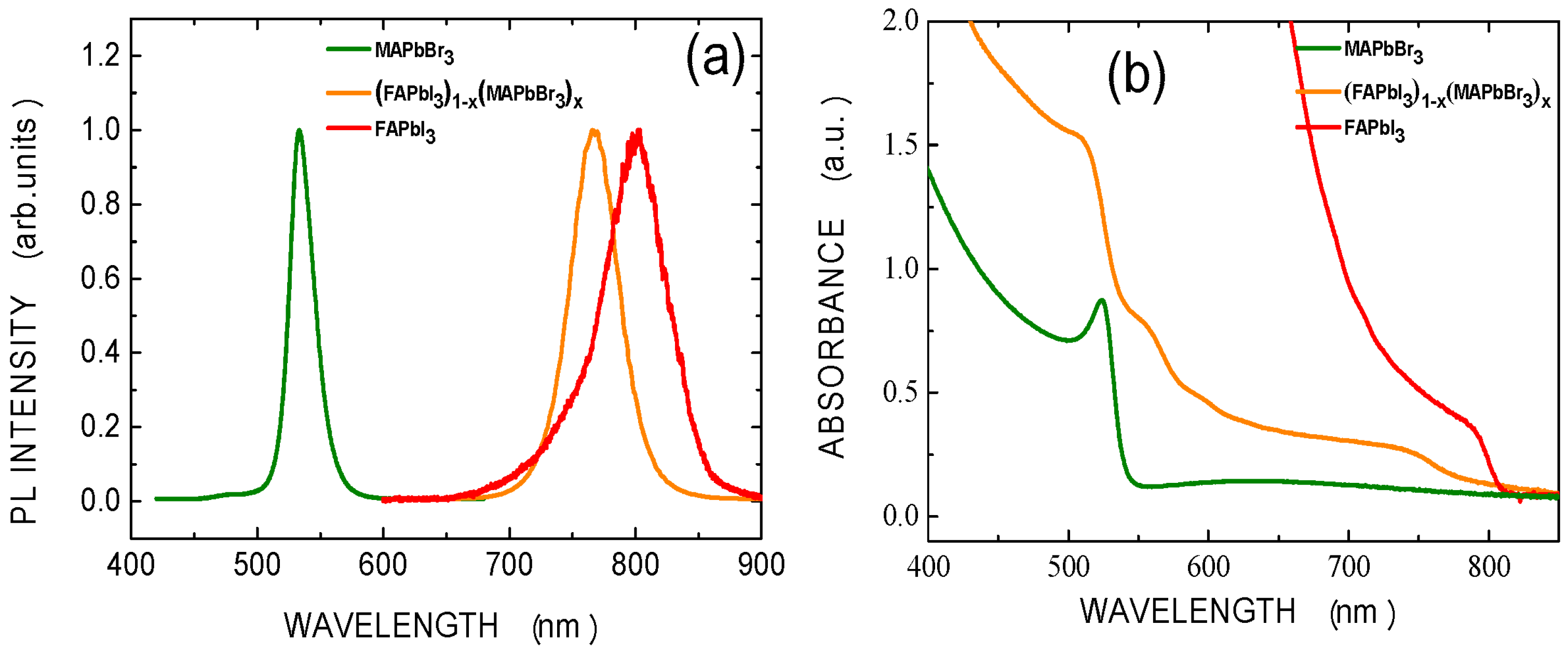
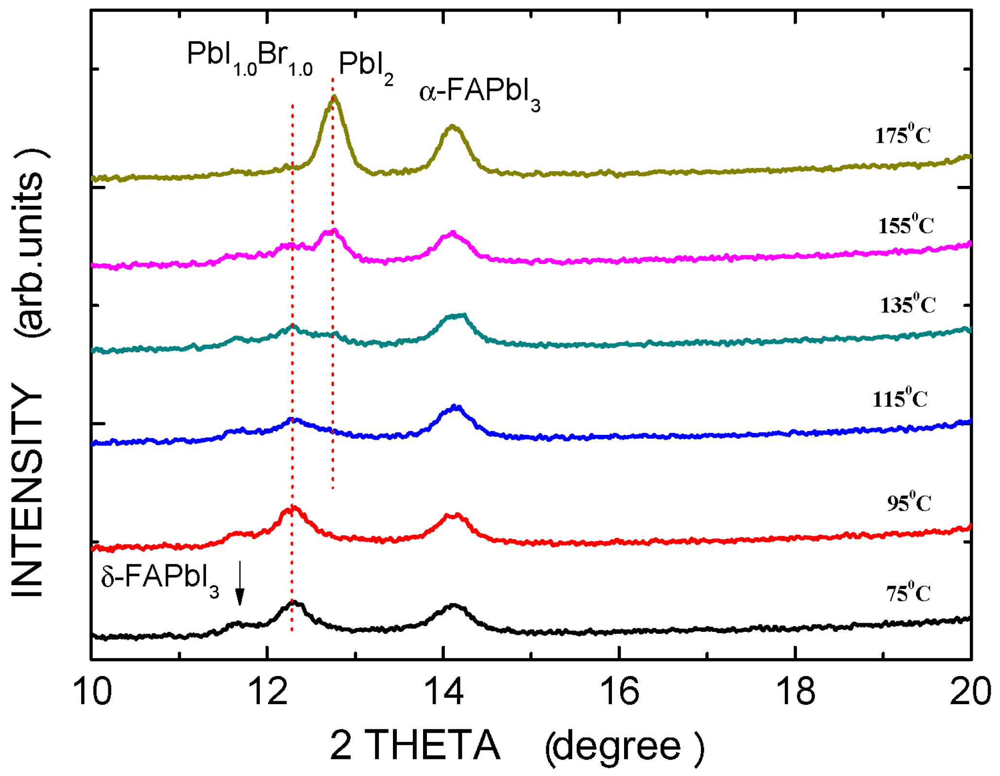
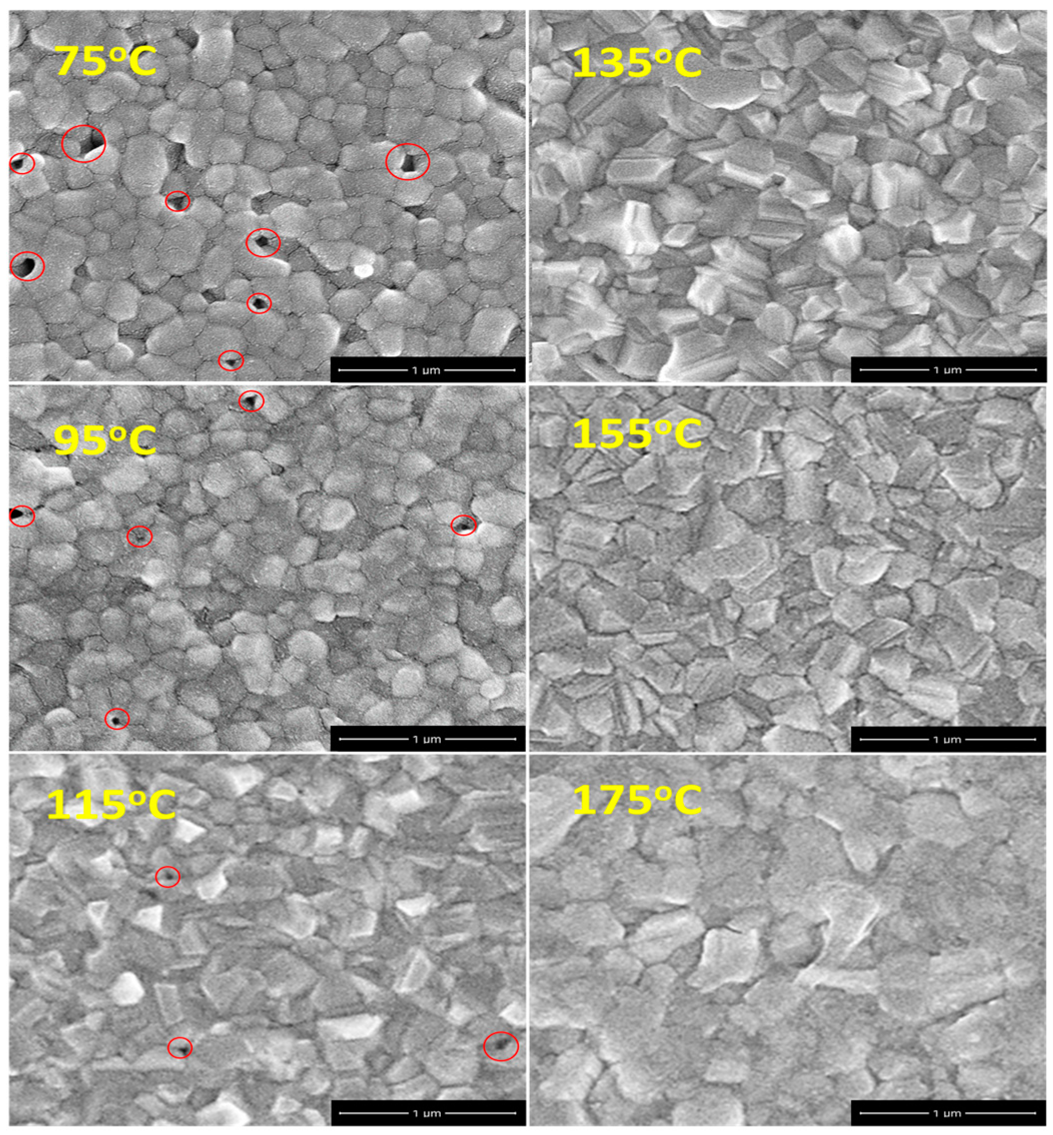
3. Results and Discussion

Mixed perovskite can be flexibly modified by changing the concentration ratio of the mixed halogen precursors [16,17]; this process is useful for photovoltaic applications. The LUMOs of FAPbI3, MAPbBr3 and C60 are −4.0, −3.6 and −3.9 eV, respectively [18,19]. To optimize the band matching with C60, the mole ratio of FAPbI3 to MAPbBr3 in the mixed perovskite was set to 80:20 (i.e., x = 0.2) because the LUMO of the (FAPbI3)0.8(MAPbBr3)0.2 was determined by interpolation to be −3.92, as presented in Figure 1b. Figure 2a displays the PL spectra of the MAPbBr3, (FAPbI3)1−x(MAPbBr3)x, and FAPbI3 films with annealing treatment at 135 °C. The spectra include peaks at 530, 762 and 800 nm, respectively. The ratio of the concentration of the (FAPbI3)1−x(MAPbBr3)x film, x, is estimated to be around 0.2 which is similar to the mole ratio in the precursor solution. The absorption edges of the three perovskite films are clearly shifted, as shown in Figure 2b.
Figure 3 shows the XRD patterns of (FAPbI3)1−x(MAPbBr3)x perovskite films after thermal annealing at various temperatures. The spectra include four main diffraction peaks at 11.67°, 12.28°, 12.71°, and 14.11°, which correspond to the δ-FAPbI3, PbI1.0Br1.0, PbI2, and α-FAPbI3 phases, respectively. As the annealing temperature increases, the intensity of the α-FAPbI3 phase peak increases and that of the δ-FAPbI3 phase peak decreases because δ-FAPbI3 transitions to the α-FAPbI3 phase or the crystallinity of the α-FAPbI3 phase is increased. Annealing at 175 °C completely suppresses the formation of the δ-FAPbI3 phase, suggesting that perovskite films must be thermally annealed to drive the inter-diffusion of precursors [20]. The δ-FAPbI3 powders can also be converted to α-FAPbI3 powders by annealing and this process is reversible even after the δ-FAPbI3 powders have been stored in air for 10 h [16]. The peak intensity of the PbI1.0Br1.0 phase decreased as the annealing temperature increased, vanishing at 175 °C, whereas the peak intensity of the PbI2 phase increased with an annealing temperature over 135 °C, perhaps because methylammonium bromide (MABr) and methylammonium iodide (MAI) were thermally decomposed from the films, forming the PbI2 phase. Furthermore, the intensity of the α-FAPbI3 phase peak increased with the annealing temperature owing to the stability of formamidinium iodide (FAI) at high temperatures.
Figure 4 presents SEM images of (FAPbI3)1−x(MAPbBr3)x perovskite films that have been thermally annealed at various temperatures. The grain size increased with the annealing temperature. A smooth, dense perovskite film was obtained when the annealing temperature exceeded 135 °C. Lower annealing temperatures yielded rough films with some defects (or pinholes). A high-quality perovskite film is crucial in the fabrication of well-performing photovoltaic devices, as revealed by the SEM micrographs in Figure 4. Clearly, the grains merged into each other as more PbI2 was formed at the grain boundaries as the annealing temperature rose above 175 °C, increasing the scattering of carriers, and thereby reducing the mobility of carriers during their transportation in the perovskite film [21].
Figure 5a displays the room-temperature PL spectra of (FAPbI3)1−x(MAPbBr3)x that was deposited on glass substrates following annealing at various temperatures. Table 1 presents the peak positions. As the annealing temperature increases from 75 to 175 °C, the PL peak shifts from 762.1 to 782.5 nm. Figure 5b shows the absorption spectra from 400 to 800 nm of (FAPbI3)1−x(MAPbBr3)x that was deposited on glass substrates following annealing at various temperatures. The absorption increased with the annealing temperature because the grains became larger (Figure 4). The inset presents an enlarged view of Figure 5b. The PL observations indicate that the absorption edges shift to longer wavelengths as the annealing temperature increases, owing to an offset of the stoichiometric ratio of α-FAPbI3 to MAPbBr3 since more α-FAPbI3 is formed and transitions to δ-FAPbI3 and more MAI and MABr decompose in the films. Therefore, the semiconducting band gap of the films downshifts to approaching that of the pure α-FAPbI3 phase. This result reveals that the composition of mixed perovskite is extremely sensitive to the temperature of annealing.
Figure 6a plots the current density as a function of the voltage (J-V) of solar cells that are based on (MAPbBr3)x(FAPbI3)1−x and annealed at various temperatures. Table 2 presents the power conversion efficiency (Eff), short-circuit current density (Jsc), open-circuit voltage (Voc) and fill factor (FF) of the (MAPbBr3)x(FAPbI3)1−x solar cells. At annealing temperatures of less than 135 °C, the power conversion efficiency increased with the annealing temperature because Jsc increased as the strength of the absorption and the amount of α-FAPbI3 formed increased. An annealing temperature of 135 °C maximized the power conversion efficiency of the cell. The optimal device, formed by annealing at 135 °C, exhibited an outstanding performance, with Jsc = 20.6 mA/cm2, Voc = 0.88 V, FF = 65.9%, and Eff = 12.0%.
The band gap of the (MAPbBr3)x(FAPbI3)1−x film is reduced as more of the α-FAPbI3 phase is formed in the films (Figure 5). Therefore, annealing at 135 °C reduces the LUMO of the (MAPbBr3)x(FAPbI3)1−x film to match that of the C60 layer and reduces the energy barrier to the transportation of electrons, resulting in a high FF. The value of Voc is positively correlated with the difference between the HOMO of the (MAPbBr3)x(FAPbI3)1−x film and the LUMO of the C60 layer (Figure 1b) [15]. Therefore, the Voc following annealing at 135 °C is determined by the increase in the HOMO of the (MAPbBr3)x(FAPbI3)1−x film. However, annealing at temperatures above 135 °C worsens the performance of the solar cell. The band gap of (MAPbBr3)x(FAPbI3)1−x film continues to fall as the annealing temperature increases, reducing the Voc. Moreover, the LUMO level of (MAPbBr3)x(FAPbI3)1−x film is lower than that of C60, so an energy barrier is formed, lowering the FF. As mentioned above, the PbI2 phase is observed, and this may block carriers, providing another cause of the low FF and the main cause of the sudden reduction of Jsc at an annealing temperature of 175 °C.
Figure 6b shows the IPCE of the best device and the integrated current density that is calculated from IPCE data is 19.4 mA/cm2. The difference between the current density from the IPCE data and that obtained from the J-V curves is only 5.8%. Therefore, the current density data are reliable. Figure 6c plots the J-V curves of the best cell under forward and reverse scanning under AM 1.5 G illumination. The efficiency difference between the forward and reverse scans is only 3.2% (Effforward = 12.0% and Effreverse = 12.4%). The hysteresis in our case is much weaker than has been reported elsewhere [16,22], indicating that high-quality (MAPbBr3)x(FAPbI3)1−x films were formed herein by annealing.

4. Conclusions

In summary, the characteristics of (FAPbI3)1−x (MAPbBr3)x perovskite films that were thermally annealed at temperatures from 75 to 175 °C were elucidated. The optimal device that was obtained by annealing at 135 °C performed outstandingly, with short-circuit current density (Jsc) = 20.6 mA/cm2, open-circuit voltage (Voc) = 0.88 V, fill factor (FF) = 65.9%, and power conversion efficiency (Eff) = 12.0%. The (FAPbI3)1−x(MAPbBr3)x perovskite films must be thermally annealed to drive the interdiffusion that causes δ-FAPbI3 to transition into the α-FAPbI3 phase. PL and absorption studies reveal a shift in the band gap of the mixed perovskite following annealing. The composition of the mixed (FAPbI3)1−x(MAPbBr3)x perovskite system is extremely sensitive to the temperature of annealing. Therefore, the annealing of mixed (FAPbI3)1−x(MAPbBr3)x perovskite is important to control the quality of a film of that material and (ensuring OR providing) band matching in the device.

Acknowledgments

Financial support of this paper was provided by the Ministry of Science and Technology of the Republic of China under Contract No. MOST 105-2221-E-027-055.

Author Contributions

L.-C.C. wrote the paper, designed the experiments, and analyzed the data. J.-R.W., Z.-L.T., C.-C.C., S.-H.C., and J.-K.H. prepared the samples and did all the measurements. K.-L.L. and H.-M.C. made discussion and suggested parameter. All authors read and approved the final manuscript.

Conflicts of Interest

The authors declare no conflicts of interest.

References

  1. Hodes, G. Perovskite-Based Solar Cells. Science 2013, 342, 317–318. [Google Scholar] [CrossRef] [PubMed]
  2. Park, N.G. Organometal perovskite light absorbers toward a 20% efficiency low-cost solid-state mesoscopic solar cell. J. Phys. Chem. Lett. 2013, 4, 2423–2429. [Google Scholar] [CrossRef]
  3. Snaith, H.J. Perovskites: The emergence of a new era for low-cost, high-efficiency solar cells. J. Phys. Chem. Lett. 2013, 4, 3623–3630. [Google Scholar] [CrossRef]
  4. Yang, W.S.; Noh, J.H.; Jeon, N.J.; Kim, Y.C.; Ryu, S.; Seo, J.; Seok, S.I. High-performance photovoltaic perovskite layers fabricated through intramolecular exchange. Science 2015, 348, 1234–1237. [Google Scholar] [CrossRef] [PubMed]
  5. Lee, M.M.; Teuscher, J.; Miyasaka, T.; Murakami, T.N.; Snaith, H.J. Efficient hybrid solar cells based on meso-superstructured organometal halide perovskites. Science 2012, 338, 643–647. [Google Scholar] [CrossRef] [PubMed]
  6. Liu, M.; Johnston, M.B.; Snaith, H.J. Efficient planar heterojunction perovskite solar cells by vapour deposition. Nature 2013, 501, 395–398. [Google Scholar] [CrossRef] [PubMed]
  7. Kojima, A.; Teshima, K.; Shirai, Y.; Miyasaka, T. Organometal halide perovskites as visible-light sensitizers for photovoltaic cells. J. Am. Chem. Soc. 2009, 131, 6050–6051. [Google Scholar] [CrossRef] [PubMed]
  8. Research Cell Efficiency Records of National Renewable Energy Laboratory (NREL). Available online: http://www.nrel.gov/ncpv/images/efficiency_chart.jpg (accessed on 9 March 2016).
  9. Chen, Q.; Zhou, H.; Hong, Z.; Luo, S.; Duan, H.S.; Wang, H.H.; Liu, Y.; Li, G.; Yang, Y. Planar heterojunction perovskite solar cells via vapor-assisted solution process. J. Am. Chem. Soc. 2014, 136, 622–625. [Google Scholar] [CrossRef] [PubMed]
  10. Liu, D.; Kelly, T.L. Perovskite solar cells with a planar heterojunction structure prepared using room-temperature solution processing techniques. Nat. Photonics 2014, 8, 133–138. [Google Scholar] [CrossRef]
  11. Im, J.H.; Jang, I.H.; Pellet, N.; Grätzel, M.; Park, N.G. Growth of CH3NH3PbI3 cuboids with controlled size for high-efficiency perovskite solar cells. Nat. Nanotechnol. 2014, 9, 927–932. [Google Scholar] [CrossRef] [PubMed]
  12. Burschka, J.; Pellet, N.; Moon, S.J.; Humphry-Baker, R.; Gao, P.; Nazeeruddin, M.K.; Gratzel, M. Sequential deposition as a route to high-performance perovskite-sensitized solar cells. Nature 2013, 499, 316–319. [Google Scholar] [CrossRef] [PubMed]
  13. Jeon, N.J.; Noh, J.H.; Kim, Y.C.; Yang, W.S.; Ryu, S.; Seok, S.I. Solvent engineering for high-performance inorganic–organic hybrid perovskite solar cells. Nat. Mater. 2014, 13, 897–903. [Google Scholar] [CrossRef] [PubMed]
  14. Tseng, Z.L.; Chiang, C.H.; Wu, C.G. Surface engineering of ZnO thin film for high efficiency planar perovskite solar cells. Sci. Rep. 2015, 5, 13211. [Google Scholar] [CrossRef] [PubMed]
  15. Jeng, J.Y.; Chiang, Y.F.; Lee, M.H.; Peng, S.R.; Guo, T.F.; Chen, P.; Wen, T.C. CH3NH3PbI3 perovskite/fullerene planar-heterojunction hybrid solar cells. Adv. Mater. 2013, 25, 3727–3732. [Google Scholar] [CrossRef] [PubMed]
  16. Jeon, N.J.; Noh, J.H.; Yang, W.S.; Kim, Y.C.; Ryu, S.; Seo, J.; Seok, S.I. Compositional engineering of perovskite materials for high-performance solar cells. Nature 2015, 517, 476–480. [Google Scholar] [CrossRef] [PubMed]
  17. Kulkarni, S.A.; Baikie, T.; Boix, P.P.; Yantara, N.; Mathews, N.; Mhaisalkar, S. Band-gap tuning of lead halide perovskites using a sequential deposition process. J. Mater. Chem. A 2014, 2, 9221–9225. [Google Scholar] [CrossRef]
  18. Aharon, S.; Dymshits, A.; Rotem, A.; Etgar, L. Temperature dependence of hole conductor free formamidinium lead iodide perovskite based solar cells. J. Mater. Chem. A 2015, 3, 9171–9178. [Google Scholar] [CrossRef]
  19. Schueppel, R.; Schmidt, K.; Uhrich, C.; Schulze, K.; Wynands, D.; Brédas, J.L.; Brier, E.; Reinold, E.; Bu, H.B.; Baeuerle, P.; et al. Optimizing organic photovoltaics using tailored heterojunctions: A photoinduced absorption study of oligothiophenes with low band gaps. Phys. Rev. B 2008, 77, 085311. [Google Scholar] [CrossRef]
  20. Chen, L.C.; Chen, C.C.; Chen, J.C.; Wu, C.G. Annealing effects on high-performance CH3NH3PbI3 perovskite solar cells prepared by solution-process. Sol. Energy 2015, 122, 1047–1051. [Google Scholar] [CrossRef]
  21. Brandt, R.E.; Stevanović, V.; Ginley, D.S.; Buonassisi, T. Identifying defect-tolerant semiconductors with high minority-carrier lifetimes: Beyond hybrid lead halide perovskites. MRS Commun. 2015, 5, 265–275. [Google Scholar] [CrossRef]
  22. Snaith, H.J.; Abate, A.; Ball, J.M.; Eperon, G.E.; Leijtens, T.; Noel, N.K.; Stranks, S.D.; Wang, J.T.W.; Wojciechowski, K.; Zhang, W. Anomalous hysteresis in perovskite solar cells. J. Phys. Chem. Lett. 2014, 5, 1511–1515. [Google Scholar] [CrossRef] [PubMed]
Figure 1. (a) Schematically depicts the complete structure and (b) corresponding energy band diagram in this study.
Materials 09 00747 g001
Figure 2. (a) PL and (b) absorption spectra of MAPbBr3, (FAPbI3)1−x(MAPbBr3)x, and FAPbI3 films deposited on glass substrates.
Materials 09 00747 g002
Figure 3. XRD patterns of (FAPbI3)0.8(MAPbBr3)0.2 perovskite films following annealing at various temperatures.
Materials 09 00747 g003
Figure 4. SEM images of (FAPbI3)0.8(MAPbBr3)0.2 perovskite films annealed at various temperatures. Red circles indicate defect sites.
Materials 09 00747 g004
Figure 5. (a) PL and (b) absorbance spectra of perovskite films annealed at various temperatures.
Materials 09 00747 g005
Figure 6. (a) Photocurrent J-V curves of perovskite solar cell (Ag/BCP/C60/(FAPbI3)0.8(MAPbBr3)0.2/PEDOT:PSS/ITO) obtained under standard 1 sun AM 1.5 simulated solar irradiation; (b) IPCE spectrum and (c) J-V curves of best device under forward and reverse scanning.
Materials 09 00747 g006
Table 1. Peak positions in PL spectra of (FAPbI3)1−x(MAPbBr3)x deposited on glass substrates and annealed various temperatures.
Thermal Annealing TemperaturesAs-Deposited7595115135155175
PL peak (nm)762.3762.1762.1770.6775.8780.0782.5
Table 2. Parameters of solar cells based on perovskite (FAPbI3)1−x(MAPbBr3)x film annealed at various temperatures based on at least four devices.
Temperature (°C)Number of DevicesVoc (V)Jsc (mA/cm2)FF (%)Eff (%)
7541.04 ± 0.028.9 ± 4.451.7 ± 2.44.11 ± 0.20
9560.94 ± 0.0914.2 ± 1.949.4 ± 5.96.68 ± 0.69
11580.93 ± 0.0314.9 ± 0.653.6 ± 2.57.21 ± 0.42
135100.87 ± 0.00820.1 ± 0.566.4 ± 1.211.8 ± 0.20
15580.84 ± 0.0120.3 ± 0.642.9 ± 2.17.52 ± 0.61
17560.83 ± 0.0217.2 ± 1.042.0 ± 6.46.02 ± 0.88

