
Effect of Post Treatment For Cu-Cr Source/Drain Electrodes on a-IGZO TFTs

 ,
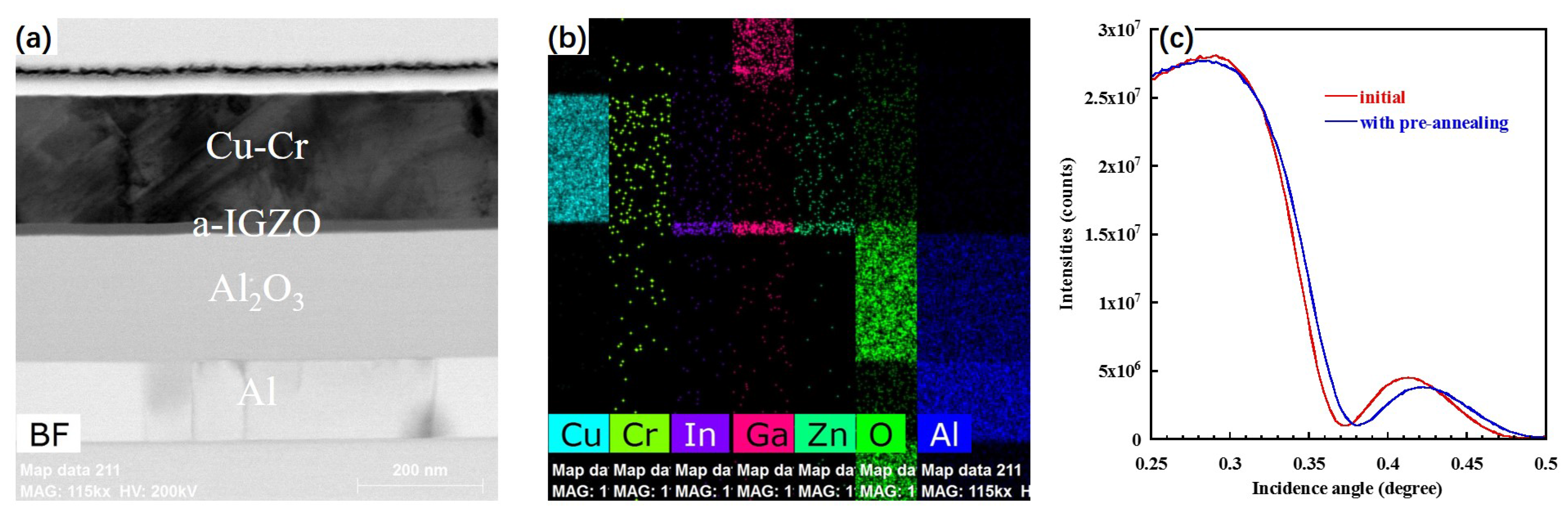
,  , , ,
, , , 
Abstract
:1. Introduction
2. Experiments
3. Results and Discussion
4. Conclusions
Acknowledgments
Author Contributions
Conflicts of Interest
References
- Liao, Y.; Shao, X.; Du, Y.; Song, Y.; Hu, W.; Zhang, Z.; Chen, Y.; Wang, Y.; Ma, Q.; Yoon, D.; et al. Development of a 120 Hz 110” ultra-high-definition a-Si liquid crystal display panel. J. Inf. Disp. 2014, 15, 77–80. [Google Scholar] [CrossRef]
- Nathan, A.; Lee, S.; Jeon, S.; Robertson, J. Amorphous Oxide Semiconductor TFTs for Displays and Imaging. J. Disp. Technol. 2014, 10, 917–927. [Google Scholar] [CrossRef]
- Matsuo, T.; Mori, S.; Ban, A.; Imaya, A. 8.3: Invited Paper: Advantages of IGZO Oxide Semiconductor. SID Symp. Dig. Tech. Pap. 2014, 45, 83–86. [Google Scholar] [CrossRef]
- Lee, S.H.; Oh, D.J.; Hwang, A.Y.; Han, D.S.; Kim, S.; Jeong, J.K.; Park, J.W. Improvement in Device Performance of a-InGaZnO Transistors by Introduction of Ca-Doped Cu Source/Drain Electrode. IEEE Electron Device Lett. 2015, 36, 802–804. [Google Scholar] [CrossRef]
- Zhao, M.; Xu, M.; Ning, H.; Xu, R.; Zou, J.; Tao, H.; Wang, L.; Peng, J. Method for Fabricating Amorphous Indium-Zinc-Oxide Thin-Film Transistors With Copper Source and Drain Electrodes. IEEE Electron Device Lett. 2015, 36, 342–344. [Google Scholar] [CrossRef]
- Jeong, J.; Lee, G.J.; Kim, J.; Choi, B. Electrical characterization of a-InGaZnO thin-film transistors with Cu source/drain electrodes. Appl. Phys. Lett. 2012, 100. [Google Scholar] [CrossRef]
- Tai, Y.H.; Chiu, H.L.; Chou, L.S. The deterioration of a-IGZO TFTs owing to the copper diffusion after the process of the source/drain metal formation. J. Electrochem. Soc. 2012, 159, J200–J203. [Google Scholar] [CrossRef]
- Yim, J.R.; Jung, S.Y.; Yeon, H.W.; Kwon, J.Y.; Lee, Y.J.; Lee, J.H.; Joo, Y.C. Effects of Metal Electrode on the Electrical Performance of Amorphous In-Ga-Zn-O Thin Film Transistor. Jpn. J. Appl. Phys. 2012, 51. [Google Scholar] [CrossRef]
- Fisher, I.; Eizenberg, M. Copper ion diffusion in porous and nonporous SiO2-based dielectrics using bias thermal stress and thermal stress tests. Thin Solid Films 2008, 516, 4111–4121. [Google Scholar] [CrossRef]
- Nagao, K.; Neaton, J.B.; Ashcroft, N.W. First-principles study of adhesion at Cu/SiO2 interfaces. Phys. Rev. B 2003, 68. [Google Scholar] [CrossRef]
- Shan, T.R.; Devine, B.D.; Phillpot, S.R.; Sinnott, S.B. Molecular dynamics study of the adhesion of Cu/SiO2 interfaces using a variable-charge interatomic potential. Phys. Rev. B 2011, 83. [Google Scholar] [CrossRef]
- Cao, Z.H.; Hu, K.; Meng, X.K. Diffusion barrier properties of amorphous and nanocrystalline Ta films for Cu interconnects. J. Appl. Phys. 2009, 106. [Google Scholar] [CrossRef]
- Park, J.S.; Kim, T.S.; Son, K.S.; Lee, E.; Jung, J.S.; Lee, K.H.; Maeng, W.J.; Kim, H.S.; Kim, E.S.; Park, K.B.; et al. Ti/Cu bilayer electrodes for SiNx-passivated Hf-In-Zn-O thin film transistors: Device performance and contact resistance. Appl. Phys. Lett. 2010, 97. [Google Scholar] [CrossRef]
- Ning, H.-L.; Hu, S.-B.; Zhu, F.; Yao, R.-H.; Xu, M.; Zou, J.-H.; Tao, H.; Xu, R.-X.; Xu, H.; Wang, L.; et al. Improved performance of the amorphous indium-gallium-zinc oxide thin film transistor with Cu-Mo source/drain electrode. Acta Phys. Sin. 2015, 64. [Google Scholar] [CrossRef]
- Lan, L.; Xu, M.; Peng, J.; Xu, H.; Li, M.; Luo, D.; Zou, J.; Tao, H.; Wang, L.; Yao, R. Influence of source and drain contacts on the properties of the indium-zinc oxide thin-film transistors based on anodic aluminum oxide gate dielectrics. J. Appl. Phys. 2011, 110. [Google Scholar] [CrossRef]
- ASTM D3359-97. Standard Test Methods for Measuring Adhesion by Tape Test; ASTM International: West Conshohocken, PA, USA, 1997. [Google Scholar] [CrossRef]
- Haynes, W.M. CRC Handbook of Chemistry and Physics; CRC Press: Boca Raton, FL, USA, 2014. [Google Scholar]


© 2016 by the authors; licensee MDPI, Basel, Switzerland. This article is an open access article distributed under the terms and conditions of the Creative Commons Attribution (CC-BY) license (http://creativecommons.org/licenses/by/4.0/).
Share and Cite
Hu, S.; Fang, Z.; Ning, H.; Tao, R.; Liu, X.; Zeng, Y.; Yao, R.; Huang, F.; Li, Z.; Xu, M.; et al. Effect of Post Treatment For Cu-Cr Source/Drain Electrodes on a-IGZO TFTs. Materials 2016, 9, 623. https://doi.org/10.3390/ma9080623
Hu S, Fang Z, Ning H, Tao R, Liu X, Zeng Y, Yao R, Huang F, Li Z, Xu M, et al. Effect of Post Treatment For Cu-Cr Source/Drain Electrodes on a-IGZO TFTs. Materials. 2016; 9(8):623. https://doi.org/10.3390/ma9080623
Chicago/Turabian StyleHu, Shiben, Zhiqiang Fang, Honglong Ning, Ruiqiang Tao, Xianzhe Liu, Yong Zeng, Rihui Yao, Fuxiang Huang, Zhengcao Li, Miao Xu, and et al. 2016. "Effect of Post Treatment For Cu-Cr Source/Drain Electrodes on a-IGZO TFTs" Materials 9, no. 8: 623. https://doi.org/10.3390/ma9080623