Article

The Resistive Switching Characteristics in ZrO2 and Its Filamentary Conduction Behavior

1
Department of Electronic Engineering, National United University, Miaoli 36063, Taiwan
2
Department and Institute of Electronic Engineering, National Kaohsiung University of Applied Sciences, Kaohsiung 80778, Taiwan
*
Author to whom correspondence should be addressed.
Materials 2016, 9(7), 551; https://doi.org/10.3390/ma9070551
Submission received: 29 May 2016 / Revised: 24 June 2016 / Accepted: 1 July 2016 / Published: 8 July 2016
(This article belongs to the Special Issue Selected Papers from ICASI 2016)

Abstract

:
This study investigated the conduction properties of sputtered ZrO2 exhibiting reversible and stable resistance change. Similar current distributions in on/off conduction and set/reset switching were observed in top electrodes with a diameter of 150, 250, and 350 µm. The size independence of current magnitude implied the presence of an uneven filamentary path over the electrode area. Increased current compliance was imposed on the turn-on process, and the observed increase in on-state current and turn-off threshold was attributed to incremental filament diameter. Variations in current conduction and resistance switching were analyzed by monitoring sweeping bias limits in both positive and negative polarities. These experimental observations were interpreted based on the aspect ratio of channels comprising conductive and oxidized filament portions, thereby elucidating the characteristics of filamentary resistive switching.

1. Introduction

Resistive random access memory (RRAM), which is a crucial class of nonvolatile memory, is an alternative to commercial floating-gate flash memory [1]. RRAM is advantageous because of its simple device structure, easy operation, and high speed. Bistable low- and high-resistance states (LRS and HRS), can be switched reversibly by applying sweeping or pulse voltages with appropriate magnitude and polarity. The set and reset operations represent transitions to an LRS or HRS, which occur at the switching thresholds of (ISET, VSET) and (IRESET, VRESET), respectively. VSET and VRESET are of the same polarity for unipolar resistance switching (URS), whereas opposite polarities are required for bipolar resistive switching (BRS). Previous studies have observed URS and BRS in numerous binary and ternary metal oxides, and the coexistence of two switching modes has been observed in several materials, including TiO2 [2], NiO [3], ZnO [4], ZrO2 [5], HfO2 [6], and Ta2O5 [7]. ZrO2 resistive thin films exhibit long retention and superior endurance in the URS and BRS modes.
Both homogeneous and filamentary types of switching have been proposed in literature. The dependence of current conduction on the electrode area is a key difference between these two switching types. By filament model, the formation of conductive filaments (CFs) in LRS comes from the low-resistance channels between the top and bottom electrodes [8]. In previous studies, spot images have been directly observed by performing probe scanning, which provides strong support for this model [9,10]. An in-between layer was embedded to improve the switching performance by enhancing the confinement of the current path [11,12]. URS and BRS differ in resistance ratio and especially in the abrupt or gradual transition to the HRS [13,14], which implies a specific reset mechanism to be involved in the CF rupture process. The physics and characteristics of CFs provide guidelines for controlling RRAM switching operations and enhancing conduction reliability. In this study, the conduction and switching dispersions in ZrO2 devices were examined by applying various current compliances and sweeping voltage ranges. Influence of these measuring conditions was interpreted in perspective of CFs, as compared with those by preparing conditions, e.g., materials, structures, and atmosphere treatment.

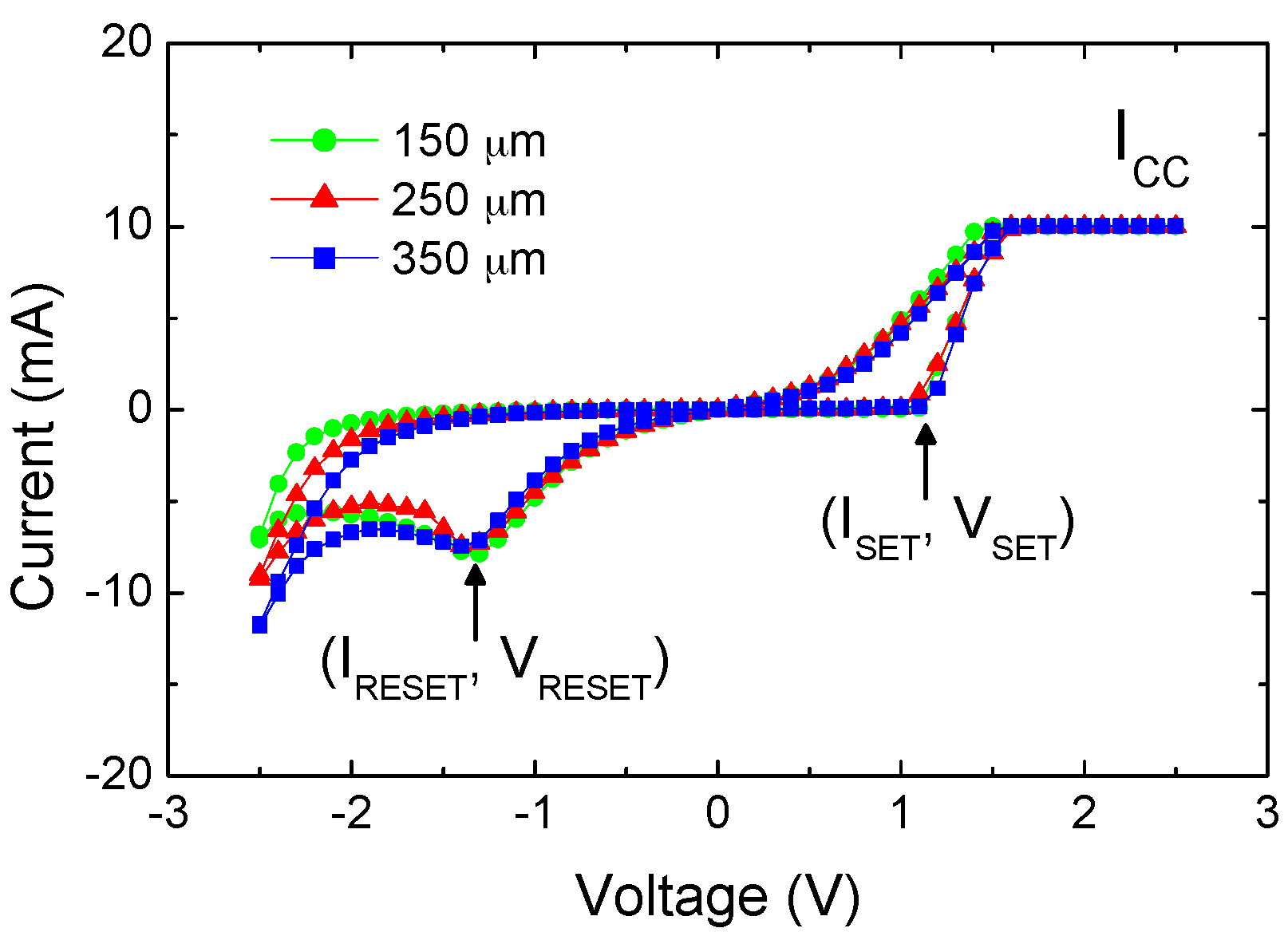
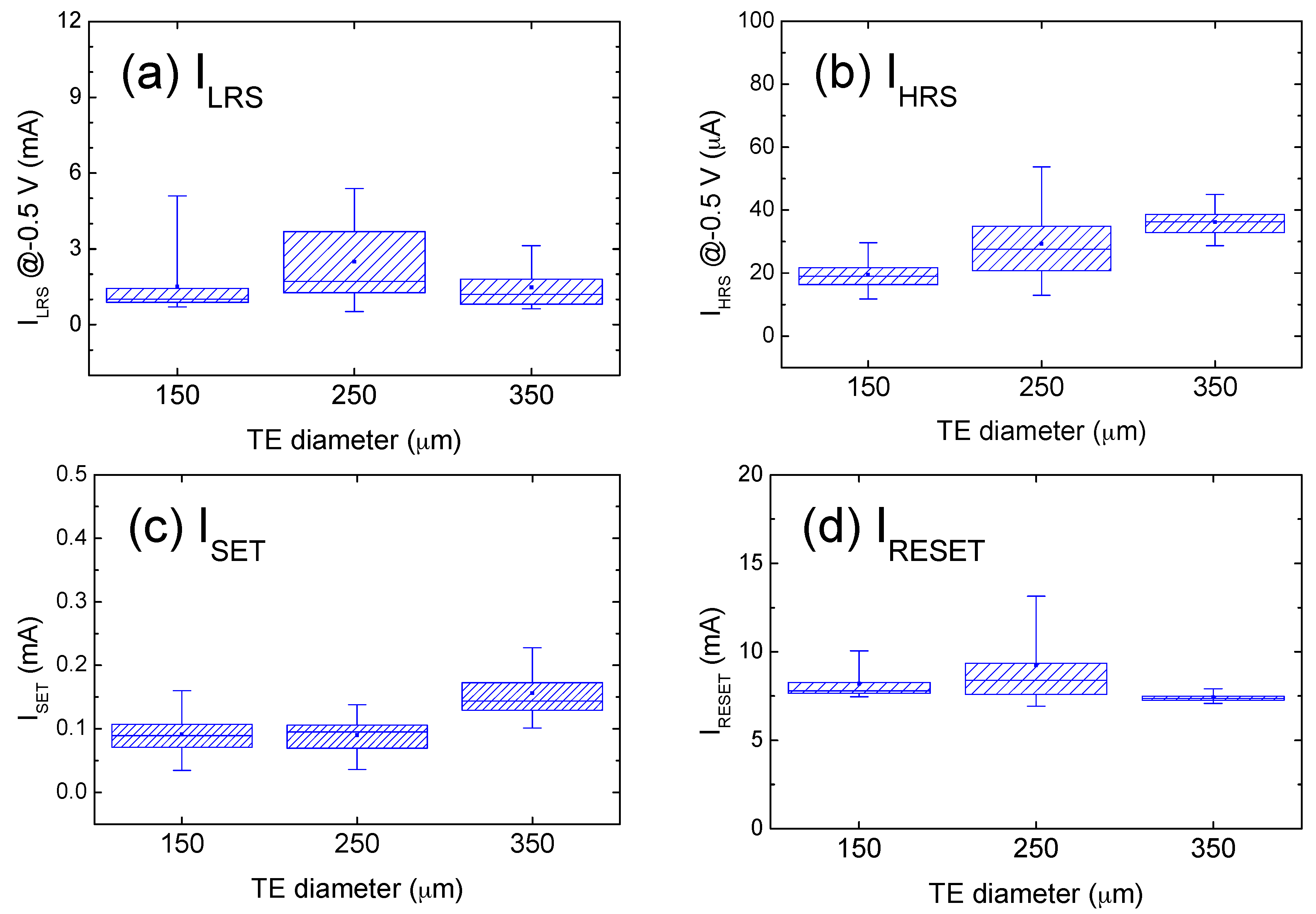
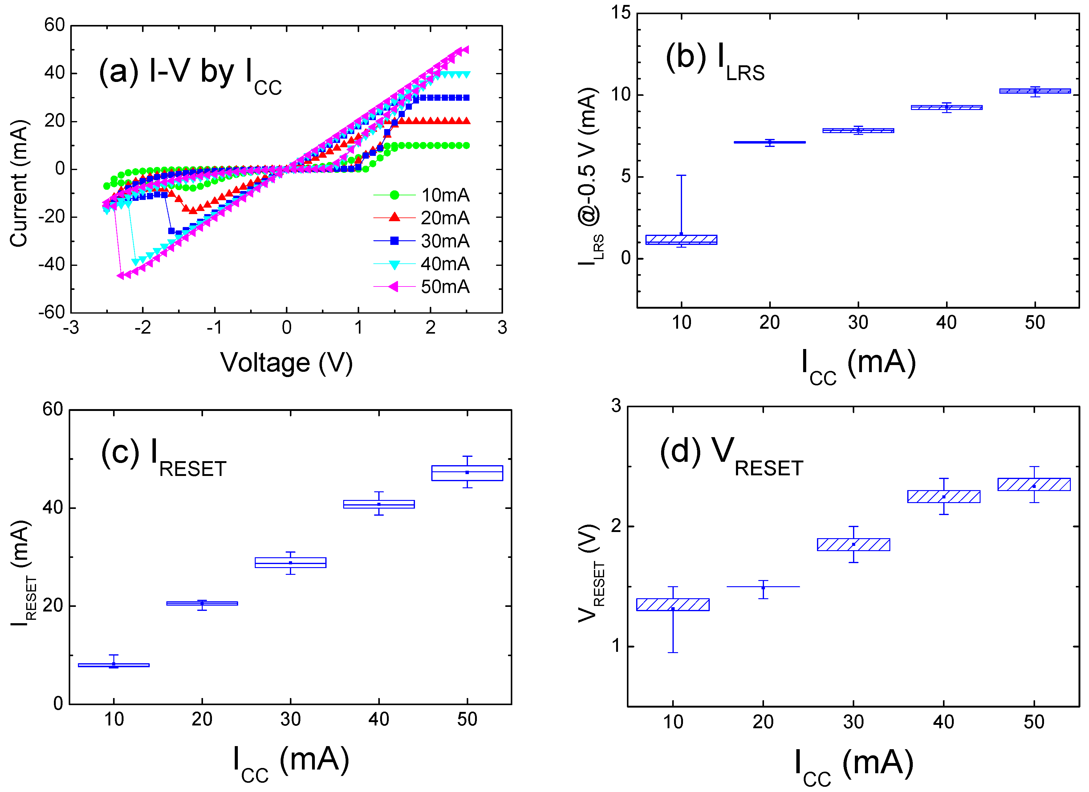
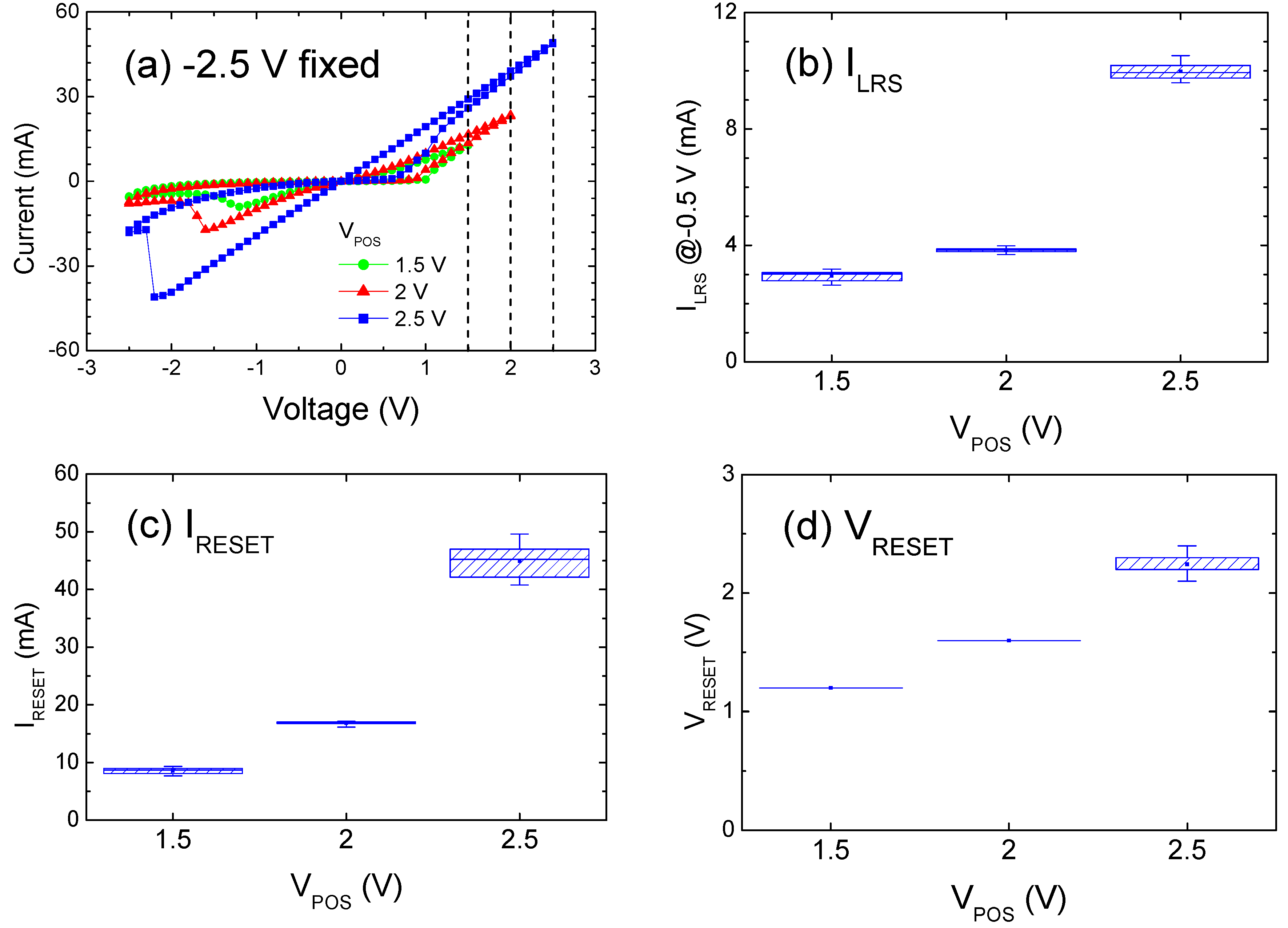
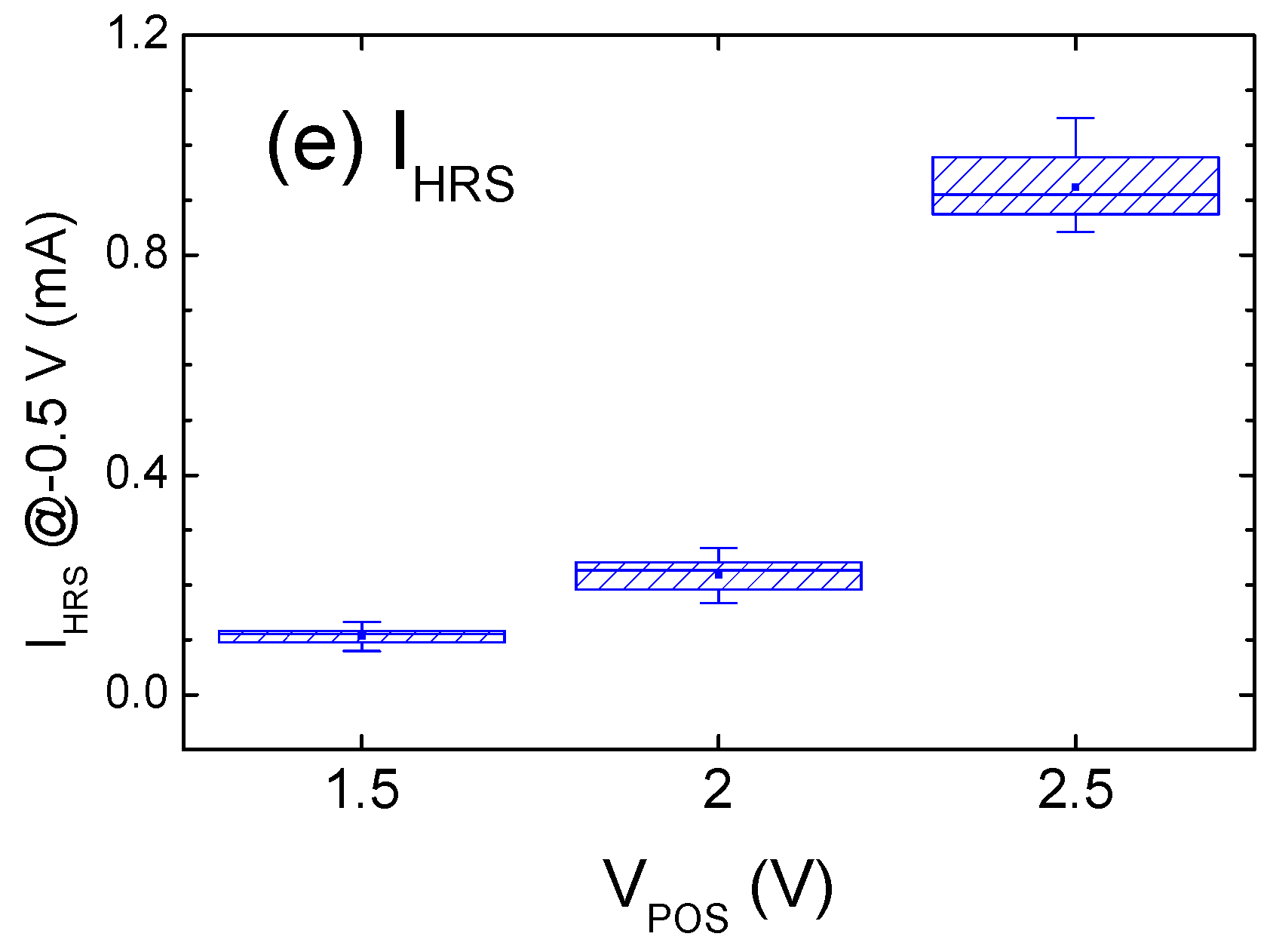
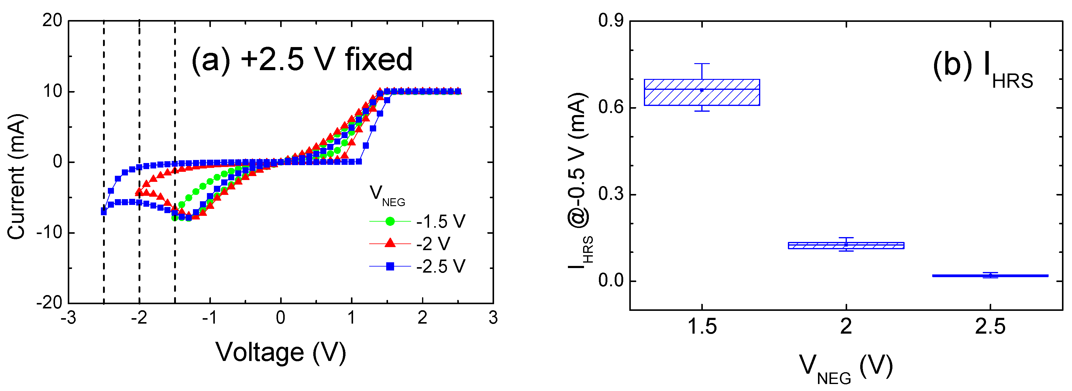
2. Results and Discussion

The device under test is of the metal-oxide-metal structure, as described in Section 3 by Ti/ZrO2/Pt. Figure 1 shows typical I–V sweeps for cells of three top electrode (TE) diameters. All of them exhibited transitions at VSET ≈ +1.1 V and VRESET ≈ −1.2 V after a forming operation at 6 V. Three crucial observations on the BRS polarity, current compliance, and current distribution are detailed as follows. First, a positive VSET polarity indicated that the reduction reaction to the LRS occurred in the ZrO2 because of higher potentials at the TE. The Ti electrode functioned as an oxygen ion getter [15], and the positively charged oxygen vacancies remained, thereby forming a low-resistance path. A detailed possible mechanism was suggested by Jeong et al. in terms of electro-chemical reaction involving oxygen ions/vacancies [16]. Once the CF formed at VSET, most of the applied current flowed through this path, and that is why ICC was applied to prevent unlimited current rise. Further increases in voltage (i.e., if VPOS was higher than VSET) and current compliance can create stronger paths or increase the CF diameter. By contrast, VRESET denotes the threshold at which resistance values begin changing. A typical gradual transition to the HRS in the BRS mode manifested as a distinct negative resistance region, which is characteristic of a CF rupture induced by oxidation processes. The extent to which the voltage sweep VNEG surpassed VRESET determined the nature of the turn-off extent. The influence of ICC and VPOS on LRS, as well as that of VNEG on HRS, is discussed in subsequent paragraph.
Second, Figure 1 shows the current compliance as a horizontal line in the upper-right corner. This compliance level was applied to prevent current overrise, to control current levels after set-switching, and to monitor the switching mode. Previous studies have adopted current compliance at the sub-milliamp scale for small cell areas (e.g., 1 µm2) [13], and even at the nano-amp scale [17]. Proper adoption of down-size cell and compliance level provides a route to the low-power switching operation of ZrO2 device. Lee et al. [4] reported a switching mode change from BRS to URS when an ICC of up to 40 mA was applied to a ZnO semiconductor with a TE diameter of 150 µm. The decision to apply ICC values higher than 10 mA in this study was based on the conduction current levels of ILRS and IHRS, as well as those obtained at VSET and VPOS. Under relatively high compliance (e.g., up to 50 mA), the studied ZrO2 devices exhibited reproducible and stable BRS properties. The increases in local temperature, known as the Joule heating effect, play a critical role in the electro-thermal process for URS. For the electro-chemical redox in BRS, this thermal impact is not discussed because of the complex nature of material thermal conductivity and filament distribution/density.
As for the third point about the current distribution extracted from Figure 1, Figure 2 shows 100 successive sweeping cycles for conduction currents (ILRS, IHRS) and switching currents (ISET, IRESET). LRS and HRS conduction currents (ILRS and IHRS) were measured at −0.5 V, at which the I–V curve exhibited a linear relationship. The figures show that I–V curves are independent from TE size by fixing ICC and (VPOS, VNEG). The size-insensitive property of ILRS was attributed to the highly localized filament that formed in the ZrO2 matrix [18], which correlated closely with the IRESET threshold for CFs to rupture. Figure 2a,b shows that the current ratio between ILRS and IHRS was approximately two orders of magnitude by 2 mA over 20 µA. Because of the considerably lower IHRS typically observed near zero bias, a larger resistance change ratio exceeding 100 was anticipated for readout voltages less than 0.5 V. Under the condition of VSET ≈ |VRESET| and |IRESET| > ISET, as shown in Figure 2c,d, a larger reset power is required than that at set switching. Rohde [19] observed that the required power was the most dominant parameter for successful switching. The higher power required to initiate a reset transition indicates a more stable conduction in LRS, as compared with that in HRS. Supporting evidence in previous studies includes experimental findings of an improved thermal disturbance immunity facilitated by longer retention in LRS, and the substantially shorter pulse width required to induce a set-switching by an electric pulse [1]. In a compact model for a filament-type RRAM device, the contrasting operational properties were reported, e.g., a gradual resistance change in reset transition while an abrupt change in set switching [20].
Figure 3a shows I–V sweeps as a function of ICC, and Figure 3b–d shows the extracted distributions of ILRS and (IRESET, VRESET). As shown in Figure 3a, higher ICC setting will induce extension on both sides of the I–V curve with clear linearity, indicating the development of an ohmic relationship followed by the CF conduction in LRS. Figure 3b shows the tendency for ILRS to increase in conjunction with ICC, which corresponds to the increasing slope of the I–V curve. The corresponding transition is distinctly more abrupt and the switching threshold (IRESET, VRESET) is higher, as evidenced by the negatively biased I–V curves shown in Figure 3a. Therefore, the distribution tends to increase with ICC, as shown in Figure 3c,d. A more detailed explanation based on the filamentary mechanism is given below.
Voltage-induced ion migration and the resulting redox process drive the set transition in the BRS mode [20]. The CF formation is caused by interfacial oxygen ion movement toward the Ti, and also by the resultant local oxygen vacancies accumulated in the ZrO2 films [21]. Recent study revealed Ti ion contribution from the TiO2 solid electrolyte [22], although Ti electrode migration was rarely reported, as compared with Ag and Cu [23,24]. Yoon el al. [10] declared that the non-uniform and uncontrolled formation of CFs over the cell area is caused by their random growth through the thermally assisted electrochemical reaction. Previous studies have ascribed the correlated increasing ILRS with ICC to the increase in filament diameter or effective area [25,26], although Guan et al. [18] stated that strong filaments with a more favorable percolation of elements are formed under higher ICC values. Noh et al. [20] argued that the filament diameter is controlled by the bias setting of polarity, amplitude, and time. They derived CF resistance as a function of filament diameter based on ohmic conduction. Moreover, McWilliams et al. [27] used equations to demonstrate that ICC correlates explicitly with resistance in the LRS and with IRESET. Contrary to the field-induced set process, the reset transition is current driven [5]. Thus, higher ICC leads to rising ILRS, and an increasing IRESET typically coincides with an increase in ILRS [27,28]. Rahaman et al. [17] plotted the linear relationship of ICC–IRESET and ICC–CF diameter. These arguments could be further verified by direct observation of the filaments [29,30].
The increasing IRESET in Figure 3c is approximately equal to ICC, and this rise surmounts that of VRESET in Figure 3d. The resultant resistance decline with ICC complies with the resistance decrease in Figure 3b, i.e., the resistance in LRS is related to the resistance at the reset threshold. Furthermore, Wang [31] observed a more abrupt reset process by increasing ICC, which similarly occurred at higher VRESET. They proposed a scheme of singly connected CFs formed under low ICC, whereas net-like CFs generated at high ICC. The reset process involves an oxidation reaction caused by oxygen ions to reenter into ZrO2; subsequently, a re-oxidized portion forms near the interface. A ruptured filament of shorter length is then connected in series with an HRS region. Park et al. [32] applied a sweeping range to examine the gradual reset transition, and confirmed the existence of incompletely dissolved CFs by performing conductive atomic force microscopy. Long et al. [33] computed reset statistics and confirmed its dependence on ILRS and, therefore, CF size, which was determined by the set or compliance setting in preceding operation. Liu et al. [34] controlled the CF growth process and overcame the intrinsic multistep reset jiggles. The manipulation of set or reset conditions to obtain multiple distinguishable LRSs or HRSs provides a potential RRAM application for multibit storage. Varying the sweeping bias limits is an effective method, as discussed in the next two paragraphs.
Because VSET is the threshold at which CFs are formed, it is a reasonable speculation that a sweep value higher than VSET would enhance CF growth. The extent to which VPOS is higher than VSET determines the filament diameter or strength. Compliance was removed to examine the VPOS effect alone. Figure 4a shows the I–V data where VPOS is 1.5, 2, and 2.5 V while −2.5 V is fixed. Similar to Figure 3, Figure 4b–d shows the extracted distributions of ILRS and (IRESET, VRESET). The impact of VPOS on the conduction in LRS is similar to that exerted by ICC, including an increase in ILRS and in the steepness of the linear I–V curve, a larger power required at reset, and a more abrupt reset transition. Regarding the relatively small increase in VRESET compared with that of IRESET (see Figure 4c,d, the decrease in resistance at the reset threshold agrees with the decreasing resistance in LRS (see Figure 4b). The similarity between the effects of ICC and VPOS was ascribed to the increase in CF diameter. Excess bias expels additional oxygen ions to the Ti reservoir and leaves an oxygen-deficient region with an enhanced cross-section. When the CFs ruptured under the same magnitude (i.e., −2.5 V) to have an identical re-oxidized length, the remaining CFs still exhibited lower resistance under the preceding VPOS values, which explains why the distribution in Figure 4e shows an increase in IHRS as VPOS increases.
Figure 5a shows the I–V sweeps under various VNEG settings. The dotted lines denote −1.5, −2, and −2.5 V, with ICC maintained at +2.5 V. Contrary to the CFs growth as a result of the VPOS extent, VNEG influenced the extension of the re-oxidized segment after reset operation. The decreasing IHRS shown in Figure 5b is primarily attributed to the highly resistive re-oxidized portion, or could be ascribed to the shortened length of partially disconnected or narrower CFs. Numerous previous studies have reported that controlling the sweeping range in the reset polarity reduces the value of IHRS [21,26,35,36,37]. Park et al. [35] successfully modulated IHRS and therefore demonstrated the feasibility of multibit applications by adjusting the value of VNEG. An engineered Schottky barrier height between Ir and TiOX explains this effect. Yu et al. [36] ascribed the decrease in IHRS to a large tunneling gap between the electrode and residual CFs, and proposed that the IHRS–VNEG mechanism is associated with the switching mode and electrode contact. In summary, the variation in the aspect ratio of the filament model presented in this study intuitively explains the difference between the values shown in Figure 4e and Figure 5b; i.e., IHRS increases in conjunction with the CF diameter, whereas IHRS declines in conjunction with CF length.

3. Materials and Methods

Sputtered ZrO2 (approximately 60-nm thick) was deposited on a Pt/Ti/SiO2/Si substrate at 250 °C and 10 mTorr under an O2: Ar gas mixture with a ratio of 6:12 and a flow rate of 18 cm3 per minute. Because of its oxygen getter properties, Ti was sputter-deposited as the top electrode (TE), and then patterned using a shadow mask with various diameters (150, 250, and 350 µm) to analyze the size effect. The devices were tested in tri-layer structures comprising Ti (110 nm)/ZrO2 (60 nm)/Pt. Current-voltage (I–V) curves were obtained using an HP4155A semiconductor parameter analyzer. Device switching between the LRS and HRS was achieved by applying a direct voltage sweep mode while the bottom electrode was grounded. Bias was applied to the TE during each sweep cycle in the range of VPOS to −VNEG, which denote the positive and negative bias limits, respectively. The current compliance ICC was set to 10–50 mA at the VSET side to control the current level in the LRS. To differentiate between the dependence of specific parameters clearly, this study refers only to their magnitudes and ignores the corresponding signs. Setting VPOS (VNEG) higher than VSET (VRESET) is necessary for successful switching. Ambient water vapor pressure is kept constant to exclude the effect of moisture on the switching characteristics [38,39]. Unless stated otherwise, the data for the I–V curves were measured at room temperature, with an ICC of 10 mA, TE diameter of 150 µm, and a sweeping range of ±2.5 V.

4. Conclusions

The effect of current compliance and sweeping range on sputtered Ti/ZrO2/Pt was investigated by examining the distributions of the corresponding I–V curves. The area independence of conduction and switching currents indicates that the formation of CFs was localized over the electrode. The on-state current and corresponding turn-off threshold increased in conjunction with the current compliance. Similar results were observed when higher VPOS values were applied. The formation of CFs with increased diameters explains these experimental observations. By contrast, extending VNEG resulted in shorter CFs and a re-oxidized portion, thereby decreasing the IHRS.

Acknowledgments

The authors thank the Ministry of Science and Technology, R.O.C., Taiwan, for financially supporting this research under Contract No. of MOST 103-2221-E-239-031.

Author Contributions

Chun-Hung Lai conceived and designed the experiments, analyzed the data and wrote the paper. Chih-Yi Lin performed the experiments, and Hung-Wei Chen contributed materials/analysis tools.

Conflicts of Interest

The authors declare no conflict of interest.

References

  1. Liu, C.Y.; Wu, P.H.; Wang, A.; Jang, W.Y.; Young, J.C.; Chiu, K.Y.; Tseng, T.Y. Bistable resistive switching of a sputter-deposited Cr-doped SrZrO3 memory film. IEEE Electron Device Lett. 2005, 26, 351–353. [Google Scholar] [CrossRef]
  2. Jeong, D.S.; Schroeder, H.; Waser, R. Coexistence of bipolar and unipolar resistive switching behaviors in a Pt/TiO2/Pt stack. Electrochem. Solid State Lett. 2007, 10, G51–G53. [Google Scholar] [CrossRef]
  3. Goux, L.; Lisoni, J.G.; Jurczak, M.; Wouters, D.J.; Courtade, L.; Muller, Ch. Coexistence of the bipolar and unipolar resistive-switching modes in NiO cells made by thermal oxidation of Ni layers. J. Appl. Phys. 2010, 107. [Google Scholar] [CrossRef]
  4. Lee, S.; Kim, H.; Park, J.; Yong, K. Coexistence of unipolar and bipolar resistive switching characteristics in ZnO thin films. J. Appl. Phys. 2010, 108. [Google Scholar] [CrossRef]
  5. Lin, C.Y.; Wu, C.Y.; Wu, C.Y.; Tseng, T.Y. Modified resistive switching behavior of ZrO2 memory films based on the interface layer formed by using Ti top electrode. J. Appl. Phys. 2007, 102. [Google Scholar] [CrossRef]
  6. Govoreanu, B.; Kar, G.S.; Chen, Y.; Paraschiv, V.; Kubicek, S.; Fantini, A.; Radu, I.P.; Goux, L.; Clima, S.; Degraeve, R.; et al. 10 × 10 nm2 Hf/HfOX crossbar resistive RAM with excellent performance, reliability and low-energy operation. IEDM Tech. Dig. 2011, 31.6.1–31.6.4. [Google Scholar]
  7. Lee, M.-J.; Lee, C. B.; Lee, D.; Lee, S.R.; Chang, M.; Hur, J. H.; Kim, Y.-B.; Kim, C.-J.; Seo, D.H.; Seo, S.; et al. A fast, high-endurance and scalable non-volatile memory device made from asymmetric Ta2O5-X/TaO2-X bilayer structures. Nat. Mater. 2011, 10, 625–630. [Google Scholar] [CrossRef] [PubMed]
  8. Jung, K.; Seo, H.; Kim, Y.; Im, H.; Hong, J.; Park, J.W.; Lee, J.K. Temperature dependence of high- and low-resistance bistable states in polycrystalline NiO films. Appl. Phys. Lett. 2007, 90. [Google Scholar] [CrossRef]
  9. Chen, X.; Wu, N.J.; Strozier, J.; Ignatiev, A. Synthesis and magnetic properties of Fe3Pt nanowire arrays fabricated by electrodeposition. Appl. Phys. Lett. 2005, 87. [Google Scholar] [CrossRef]
  10. Sun, J.; Liu, Q.; Xie, H.; Wu, X.; Xu, F. In situ observation of nickel as an xxidizable electrode material for the solid-electrolyte-based resistive random access memory. Appl. Phys. Lett. 2013, 102. [Google Scholar] [CrossRef]
  11. Liu, C.Y.; Lin, X.J.; Wang, H.Y.; Lai, C.H. Improved resistive switching dispersion of NiOX thin film by Cu-doping method. Jap. J. Appl. Phys. 2010, 49. [Google Scholar] [CrossRef]
  12. Yoon, J.H.; Han, J.H.; Jung, J.S. Highly improved uniformity in the resistive switching parameters of TiO2 thin films by inserting Ru nanodots. Adv. Mater. 2013, 25, 1987–1992. [Google Scholar] [CrossRef] [PubMed]
  13. Wang, W.; Fujita, S.; Wong, S.S. Reset mechanism of TiOX resistance-change memory device. IEEE Electron Device Lett. 2009, 30, 733–735. [Google Scholar] [CrossRef]
  14. Celano, U.; Goux, L.; Belmonte, A.; Giammaria, G.; Opsomer, K.; Detavernier, C.; Richard, O.; Bender, H.; Irrera, F.; Jurczak, M.; et al. Progressive vs. abrupt reset behavior in conductive bridging devices: A C-AFM tomography study. IEDM Tech. Dig. 2014, 14.1.1–14.1.4. [Google Scholar]
  15. Clima, S.; Sankaran, K.; Chen, Y.Y.; Fantini, A.; Celano, U.; Belmonte, A.; Zhang, L.; Goux, L.; Govoreanu, B.; Degraeve, R.; et al. RRAMs based on anionic and cationic switching: A short overview. Phys. Status Solid Rapid Res. Lett. 2014, 8, 501–511. [Google Scholar] [CrossRef]
  16. Jeong, D.S.; Schroeder, H.; Waser, R. Mechanism for bipolar switching in a Pt/TiO2/Pt resistive switching cell. Phys. Rev. B 2009, 79. [Google Scholar] [CrossRef]
  17. Rahaman, S.Z.; Maikap, S.; Chen, W.S.; Lee, H.Y.; Chen, F.T.; Tien, T.C.; Tsai, M.J. Impact of TaOX nanolayer at the GeSeX/W interface on resistive switching memory performance and investigation of Cu nanofilament. J. Appl. Phys. 2012, 111. [Google Scholar] [CrossRef]
  18. Guan, W.; Long, S.; Liu, Q.; Liu, M.; Wang, W. Nonpolar nonvolatile resistive switching in Cu doped ZrO2. IEEE Electron Device Lett. 2008, 29, 434–437. [Google Scholar] [CrossRef]
  19. Rohde, C.; Choi, B.J.; Jeong, D.S.; Choi, S.; Zhao, J.S.; Hwang, C.S. Identification of a determining parameter for resistive switching of TiO2 thin films. Appl. Phys. Lett. 2005, 86. [Google Scholar] [CrossRef]
  20. Noh, J.; Jo, M.; Kang, C.Y.; Gilmer, D.; Kirsch, P.; Lee, J.C.; Lee, B.H. Development of a semiempirical compact model for DC/AC cell operation of HfOX-based ReRAMs. IEEE Electron Device Lett. 2013, 34, 1133–1135. [Google Scholar] [CrossRef]
  21. Wang, S.Y.; Huang, C.W.; Lee, D.Y.; Tseng, T.Y.; Chang, T.C. Multilevel resistive switching in Ti/CuXO/Pt memory devices. J. Appl. Phys. 2010, 108. [Google Scholar] [CrossRef]
  22. Wedig, A.; Luebben, M.; Cho, D.Y.; Moors, M.; Skaja, K.; Rana, V.; Hasegawa, T.; Adepalli, K.K.; Yildiz, B.; Waser, R.; et al. Nanoscale cation motion in TaOX, HfOX and TiOX memristive systems. Nat. Nanotechnol. 2016, 11, 67–74. [Google Scholar] [CrossRef] [PubMed]
  23. Gao, S.; Chen, C.; Zhai, Z.; Liu, H.Y.; Lin, Y.S.; Li, S.Z.; Lu, S.H.; Wang, G.Y.; Song, C.; Zeng, F.; et al. Resistive switching and conductance quantization in Ag/SiO2/indium tin oxide resistive memories. Appl. Phys. Lett. 2014, 105. [Google Scholar] [CrossRef]
  24. Tsuruoka, T.; Valov, I.; Tappertzhofen, S.; Hurk, J.; Hasegawa, T.; Waser, R.; Aono, M. Redox reactions at Cu,Ag/Ta2O5 interfaces and the effects of Ta2O5 film density on the forming process in atomic switch structures. Adv. Funct. Mater. 2015, 25, 6374–6381. [Google Scholar] [CrossRef]
  25. Choi, S.J.; Kim, K.H.; Park, G.S.; Bae, H.J.; Yang, W.Y.; Cho, S. Multibit operation of Cu/Cu-GeTe/W resistive memory device controlled by pulse voltage magnitude and width. IEEE Electron Device Lett. 2011, 32, 375–377. [Google Scholar] [CrossRef]
  26. Puglisi, F.M.; Larcher, L.; Bersuker, G.; Padovani, A.; Pavan, P. An empirical model for RRAM resistance in low- and high-resistance states. IEEE Electron Device Lett. 2013, 34, 387–389. [Google Scholar] [CrossRef]
  27. McWilliams, C.R.; Celinska, J.; Araujo, C.A.; Xue, K.H. Device characterization of correlated electron random access memories. J. Appl. Phys. 2011, 109. [Google Scholar] [CrossRef]
  28. Hu, W.; Chen, X.; Wu, G.; Lin, Y.; Qin, N.; Bao, D. Bipolar and tri-state unipolar resistive switching behaviors in Ag/ZnFe2O4/Pt memory devices. Appl. Phys. Lett. 2012, 101. [Google Scholar] [CrossRef]
  29. Kumar, S.; Graves, C.E.; Strachan, J.P.; Grafals, E.M.; Kilcoyne, A.L.D.; Tyliszczak, T.; Weker, J.N.; Nishi, Y.; Williams, R.S. Direct observation of localized radial oxygen migration in functioning tantalum oxide memristors. Adv. Mater. 2016, 28, 2772–2776. [Google Scholar] [CrossRef] [PubMed]
  30. Celano, U.; Goux, L.; Degraeve, R.; Fantini, A.; Richard, O.; Bender, H.; Jurczak, M.; Vandervorst, W. Imaging the three-dimensional conductive channel in filamentary-based oxide resistive switching memory. Nano Lett. 2015, 15, 7970–7975. [Google Scholar] [CrossRef] [PubMed]
  31. Wang, Z.Q.; Li, X.H.; Xu, H.Y.; Wang, W.; Yu, H.; Zhang, X.T.; Liu, Y.X.; Liu, Y.C. Effects of compliance currents on the formation and rupture of conducting filaments in unipolar resistive switching of CoO film. J. Phys. D Appl. Phys. 2010, 43. [Google Scholar] [CrossRef]
  32. Park, J.; Jo, M.; Lee, J.; Jung, S.; Kim, S.; Lee, W.; Shin, J.; Hwang, H. Improved switching uniformity and speed in filament-type RRAM using lightning rod effect. IEEE Electron Device Lett. 2011, 32, 63–65. [Google Scholar] [CrossRef]
  33. Long, S.; Lian, X.; Ye, T.; Cagli, C.; Perniola, L.; Miranda, E.; Liu, M.; Suñé, J. Cycle-to-cycle intrinsic reset satistics in HfO2-based unipolar RRAM devices. IEEE Electron Device Lett. 2013, 34, 623–625. [Google Scholar] [CrossRef]
  34. Liu, Q.; Long, S.; Lv, H.; Wang, W.; Niu, J.; Huo, Z.; Chen, J.; Liu, M. Controllable growth of nanoscale conductive filaments in solid-electrolyte-based ReRAM by using a metal nanocrystal covered bottom electrode. ACS Nano 2010, 4, 6162–6168. [Google Scholar] [CrossRef] [PubMed]
  35. Park, J.; Biju, K.P.; Jung, S.; Lee, W.; Lee, J.; Kim, S.; Park, S.; Shin, J.; Hwang, H. Multibit operation of TiOX-based ReRAM by schottky barrier height engineering. IEEE Electron Device Lett. 2011, 32, 476–478. [Google Scholar] [CrossRef]
  36. Yu, S.; Jeyasingh, R.; Wu, Y.; Wong, H.-S.P. AC conductance measurement and analysis of the conduction processes in HfOX based resistive switching memory. Appl. Phys. Lett. 2011, 99. [Google Scholar] [CrossRef]
  37. Chen, M.C.; Chang, T.C.; Chiu, Y.C.; Chen, S.C.; Huang, S.Y.; Chang, K.C.; Tsai, T.M.; Yang, K.H.; Sze, S.M.; Tsai, M.J. The resistive switching characteristics in TaON films for nonvolatile memory applications. Thin Solid Films 2013, 528, 224–228. [Google Scholar] [CrossRef]
  38. Messerschmitt, F.; Kubicek, M.; Rupp, J.L.M. How does moisture affect the physical property of memristance for anionic–electronic resistive switching memories? Adv. Funct. Mater. 2015, 25, 5117–5125. [Google Scholar] [CrossRef]
  39. Lübben, M.; Karakolis, P.; Ioannou-Sougleridis, V.; Normand, P.; Dimitrakis, P.; Valov, I. Graphene-modified interface controls transition from VCM to ECM switching modes in Ta/TaOX based memristive devices. Adv. Mat. 2015, 27, 6202–6207. [Google Scholar] [CrossRef] [PubMed]
Figure 1. Typical room-temperature I–V curves in linear scale under ICC = 10 mA with top electrode diameter of 150, 250, 350 μm.
Materials 09 00551 g001
Figure 2. Distribution of critical current parameters extracted from Figure 1 after multiple measurements as a function of electrode areas. (a) ILRS; (b) IHRS; (c) ISET; (d) IRESET.
Materials 09 00551 g002
Figure 3. (a) Typical room-temperature I–V curves by top electrode (TE) diameter of 150 μm under ICC of 10 to 50 mA; (b) Distribution of extracted parameters after multiple measurements for ILRS; (c) for IRESET; and (d) for VRESET.
Materials 09 00551 g003
Figure 4. (a) Typical room-temperature I–V curves as a function of VPOS with no compliance setting; (b) Effect of VPOS on ILRS; (c) on IRESET; (d) on VRESET; and (e) on IHRS.
Materials 09 00551 g004aMaterials 09 00551 g004b
Figure 5. (a) Typical room-temperature I–V curves as a function of VNEG under ICC of 10 mA; (b) Effect of VNEG on IHRS.
Materials 09 00551 g005

