Communication

Energy Storage Characteristics of BiFeO3/BaTiO3 Bi-Layers Integrated on Si

1
Key Laboratory for Liquid−Solid Structural Evolution and Processing of Materials (Ministry of Education), School of Materials Science and Engineering, Shandong University, Jinan 250061, China
2
Suzhou Institute of Shandong University, Suzhou 215123, China
3
National Institute of Standards and Technology, Gaithersburg, MD 20899, USA
*
Author to whom correspondence should be addressed.
Materials 2016, 9(11), 935; https://doi.org/10.3390/ma9110935
Submission received: 29 September 2016 / Revised: 27 October 2016 / Accepted: 11 November 2016 / Published: 18 November 2016
(This article belongs to the Special Issue Microwave Absorbing and Energy Storage Materials)

Abstract

:
BiFeO3/BaTiO3 bi-layer thick films (~1 μm) were deposited on Pt/Ti/SiO2/(100) Si substrates with LaNiO3 buffer layers at 500 °C via a rf magnetron sputtering process. X-ray diffraction (XRD) analysis revealed that both BiFeO3 and BaTiO3 layers have a (00l) preferred orientation. The films showed a small remnant polarization (Pr ~ 7.8 μC/cm2) and a large saturated polarization (Ps ~ 65 μC/cm2), resulting in a slim polarization-electric field (P-E) hysteresis loop with improved energy storage characteristics (Wc = 71 J/cm3, η = 61%). The successful “slim-down” of the P-E loop from that of the pure BiFeO3 film can be attributed to the competing effects of space charges and the interlayer charge coupling on charge transport of the bi-layer film. The accompanying electrical properties of the bi-layer films were measured and the results confirmed their good quality.

1. Introduction

Densities of electrical energy stored in or released from a dielectric can be calculated from their characteristic dielectric displacement-electric field (D-E) curves by the formula [1]:
W c = 0 D s E d D , W d = D r D s E d D
η = W d W c ,
where Wc is the charged (stored) energy density, Wd is the discharged (released) energy density and η the energy efficiency. Ds and Dr are the saturated/maximum and remnant electrical displacements, respectively. For an ideal linear dielectric with a relative dielectric constant εr, D = ε0εrE and Dr = 0, the energy densities are given by [1]:
W c = 1 2 ε 0 ε r E max 2 ,
W d = W c = 1 2 ε 0 ε r E max 2 ,
and the efficiency η equals 1. Here ε0 is the vacuum dielectric constant, Emax is the maximum applicable electric field which increases with the breakdown field Eb (EmaxEb for an ideal dielectric). On the other hand, non-linear dielectrics like ferroelectrics usually don’t have DE or Dr = 0, hence Wc > Wd and η < 1. Nevertheless, Equation (2a) can still be used for the estimation of energy densities Wc in non-linear dielectrics, wherein εr is the average or effective dielectric constant.
To meet the demands in developing portable and integrable power electronics, thin film ceramic capacitors with a high energy storage density Wc and a high efficiency η have been intensively investigated [2,3,4]. The previous studies on thin film ceramic capacitors have been focused on lead-containing perovskite ferroelectrics, including BNZ-PT, BNT-PT and BNH-PT [5,6,7]. P-E (*) curve of a typical ferroelectric is presented in Figure 1. In this figure, the green area represents the discharged energy density (Wd), the yellow area encircled by the hysteresis loop is the energy loss (Wloss), and the charged energy density is the sum of the two, Wc = Wd + Wloss. It’s obvious that the energy storage characteristics of a ferroelectric strongly depend on the shape of its P-E loop.
In the past decade, large energy storage densities (40 J/cm3–60 J/cm3) have been reported in lead-containing ferroelectric films together with good energy efficiencies (40%–60%) [6,7,8,9]. However, the growing environment concerns on lead and the usually complex compositions of the solid solutions being used are the two major drawbacks of the lead-containing ferroelectric capacitors. In order to minimize the environmental impact and promote a manufacturing-friendly preparation process, single component lead-free perovskites have been investigated by several research groups for applications in thin film dielectric capacitors [10,11,12,13,14]. Among them, BiFeO3 and BaTiO3 films are most popular candidates [13,14]. The former has a giant saturated polarization and tunable electrical properties via strain or chemical doping, while the latter has excellent dielectric properties (large εr and high Eb) and hence has been broadly used in multi-layer ceramic capacitors (MLCC). However, large leakage currents and poor energy efficiencies associated with BiFeO3 thin films have hindered its further development for energy storage applications. On the other hand, a small saturated polarization of BaTiO3 has capped its energy densities (see Equation (1a)) and limited most of its capacitor applications in MLCC.
According to Equation 1, dielectrics with high Eb and εr, a small remnant polarization and a large saturated polarization are ideal for high efficiency energy-storage applications. In this work, we demonstrate a novel approach to compensate for the lack of a single material with the above properties. We prepared ferroelectric bilayers of BiFeO3/BaTiO3 on Si substrates via an in-situ rf magnetron sputtering process at 500 °C. Textured growth of the bi-layer films at this moderate temperature was promoted by using a LaNiO3 template layer. The resulted thin film capacitors of Au/BiFeO3/BaTiO3/LaNiO3/Pt/Ti not only showed good dielectric properties (high εr and low leakage current), but also a slim P-E hysteresis featuring an enhanced energy storage density and efficiency, as compared with those of single layers of BiFeO3 and BaTiO3 on Si. The improved energy storage characteristics are interpreted based on our understanding of the charge transport process, which is dominated by the effect of space charges at low electric fields and by the interface charge coupling at high electric fields.

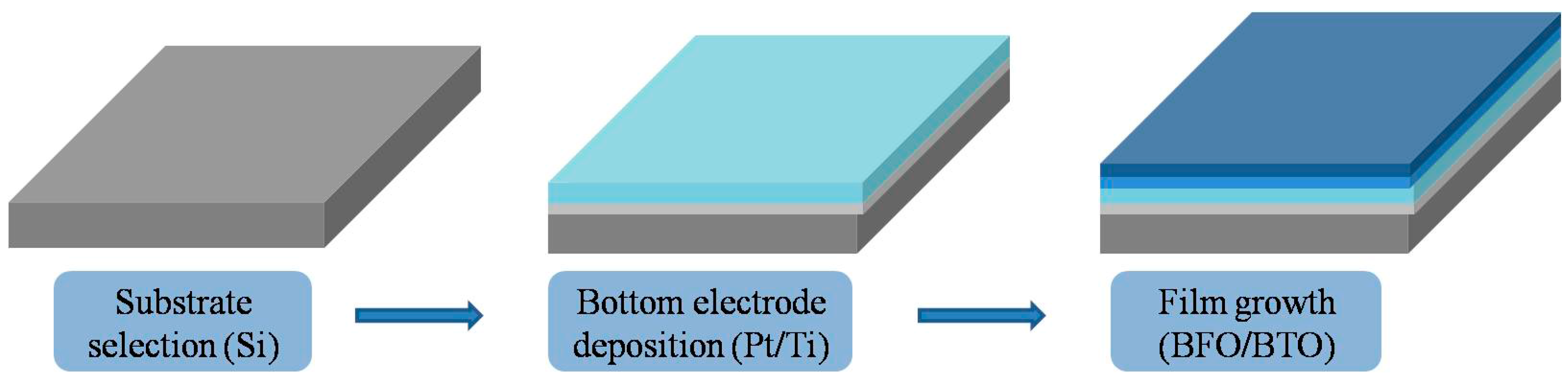
2. Experimental Section

BiFeO3/BaTiO3 bi-layer thick films were fabricated on Pt/Ti/SiO2/(100)Si substrates buffered with a LaNiO3 layer via a rf magnetron sputtering process. Commercially available ceramic targets of BaTiO3, Bi1.05FeO3 and LaNiO3 (4N purity, Ф = 50 mm, L = 5 mm) were used in the deposition process, which was carried out in a multi-target magnetron sputtering system with a base pressure of 2.0 × 10⁻⁴ Pa. Firstly, a 120-nm-thick Pt/Ti layer was deposited as the bottom electrode at 300 °C in a pure argon atmosphere. Then the LaNiO3, BaTiO3 and BiFeO3 layers were sequentially sputtered at 500 °C in a mixed gas of Ar and O2. The thickness of the BiFeO3/BaTiO3 bi-layer was about 1 μm with a 1:1 thickness ratio. Lastly, the as-deposited multi-layer thick film was cooled down at a rate of 6 °C/min–8 °C/min in pure oxygen. The deposition parameters of the sputtering process were summarized in Table 1 and the schematics of experimental procedures was shown in Figure 2. For electrical characterizations, circular Au top electrodes with a diameter of 200 μm were deposited at room temperature by using a shadow mask.
The phase structures and crystallographic orientations of the bilayer films were characterized by using X-ray diffraction (XRD) θ-2θ scans with a Ni-filtered Cu-Kα radiation resource (Dmax-rc, Monaghan, Ireland) and pole figures (R-156 Axis Spider, SmartLab® Rigaku, Tokyo, Japan, 40 kV, 200 mA). A commercially available MicroNano D-5A Scanning Probe Microscope (SPM) (MicroNano, Shanghai, China) was used to analyze the surface morphology while the cross-sectional thin film morphology was analyzed by using a thermal field emission scanning electron microscope (SEM) (SU-70, HITACHI, Hitachi, Japan) The room temperature ferroelectric hysteresis loops (P-V) and leakage currents (I-V) were measured by using a Radiant Precision Premium II ferroelectric tester (Radiant Technology, Albuquerque, NM, USA). The dielectric properties were measured by using a high precision digital bridge (QuadTech 7600 Plus Precision LCR Meter, IET LABS, Inc., West Roxbury, MA, USA).

3. Results

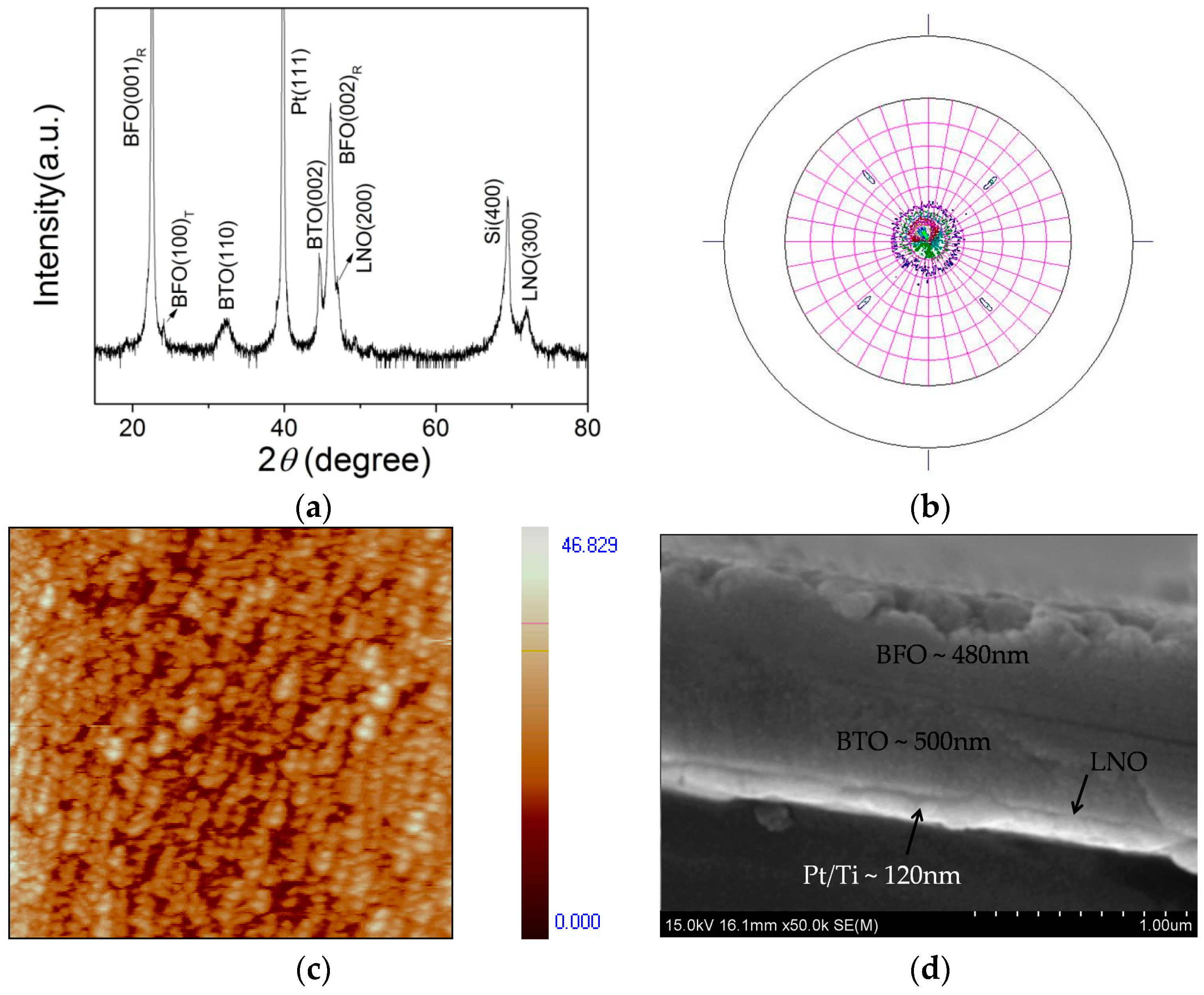
3.1. Microstructures and Crystallographic Orientations

Figure 3a shows the XRD 2θ scan spectrum of the BiFeO3/BaTiO3 bilayer film grown on LaNiO3/Pt/Ti/SiO2/(100) Si, which is dominated by the preferred (00l) diffraction peaks of the bulk perovskite structures and does not show any crystalline impurities or secondary phases. A tiny amount of (110)-oriented BaTiO3 grains and (100)-oriented tetragonal BiFeO3 grains were detected, which can be attributed to the moderate growth temperature and the effect of residual stress [15,16]. In our previous work [17], it was revealed that a highly (00l)-oriented BaTiO3 thin film can be grown on Pt/Ti/SiO2/(100) Si substrate by using a LaNiO3 buffer layer at 500 °C. Here it is confirmed that the presence of a (l00)-oriented LaNiO3 buffer layer promoted the growth of a (00l) oriented BiFeO3/BaTiO3 bi-layer film.
To further investigate the crystallographic characteristics of the bi-layer film, pole figure analysis was carried out on the {001} BiFeO3 reflection (2θ = 22.56°). During collection of the XRD signals, the sample was rotated by varying the tilt angle (0° < ψ < 70°) and the azimuthal angle (0° < φ < 360°) with respect to the scattering vector. The pole figure of (001)BFO, as shown in Figure 3b, revealed a strong diffraction peak at the center (tilt angle ψ = 0°), and a set of 4-fold diffraction peaks at ψ ≈ 46°, corresponding to the {101} BiFeO3 plane. This result confirmed the preferred (00l) orientation of the BiFeO3 layer, as suggested by the result of the XRD 2θ scans.
Surface morphology of the BiFeO3/BaTiO3 bi-layer film is displayed in Figure 3c. It can be seen that the grains of the top BiFeO3 layer are densely packed with an average size of ~200–300 nm. The surface roughness Ra was measured to be ~4.1 nm, which shows a significant reduction as compared with those of the single layer BiFeO3 films (Ra is on the order of ~10 nm or above) [18,19,20,21]. The dense and smooth growth of the BiFeO3 layer can be attributed to the good quality perovskite underlayers of LaNiO3/BaTiO3. In Figure 3d, the cross-sectional SEM image shows clean and sharp interfaces in the multi-layer thin film. The BiFeO3 and BaTiO3 layers were measured to be ~480 nm and ~500 nm, respectively.

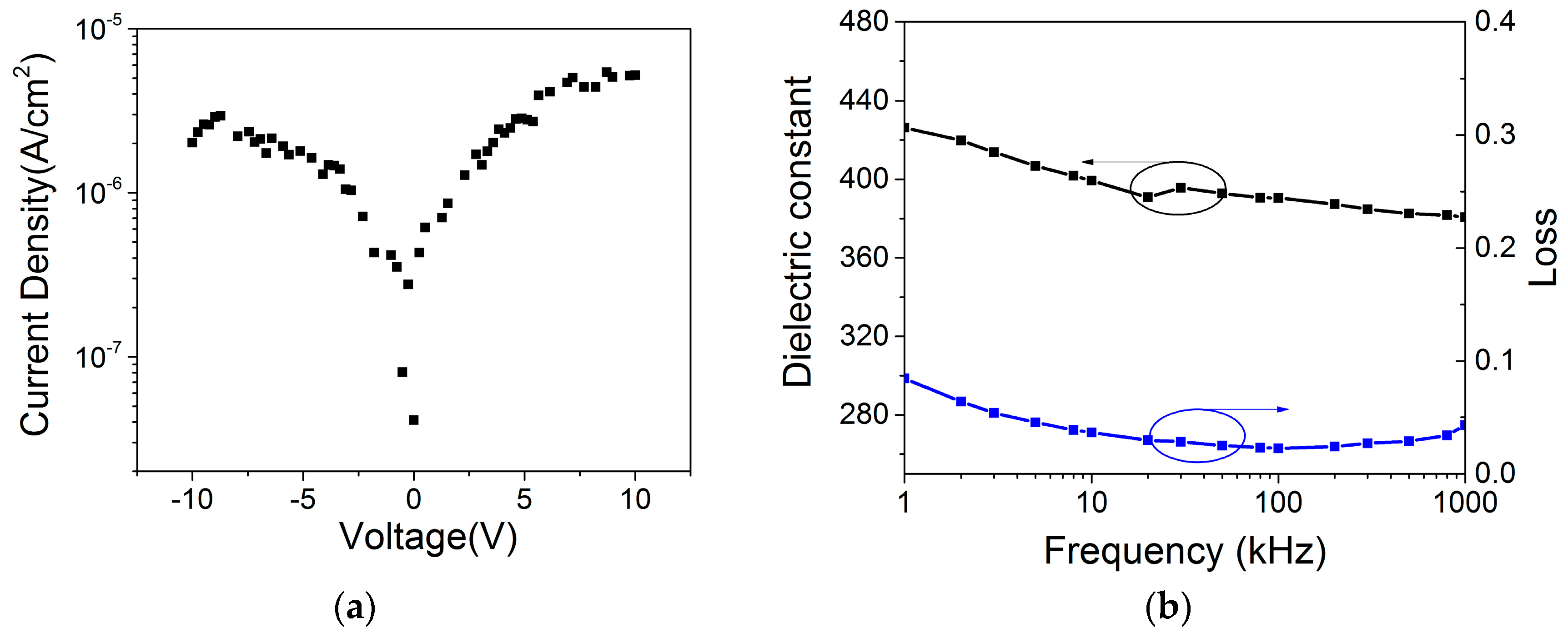
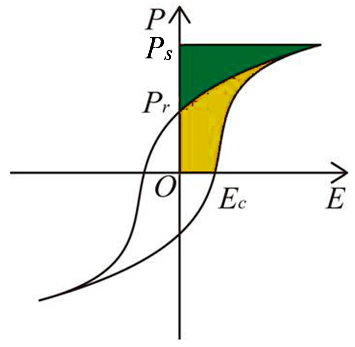
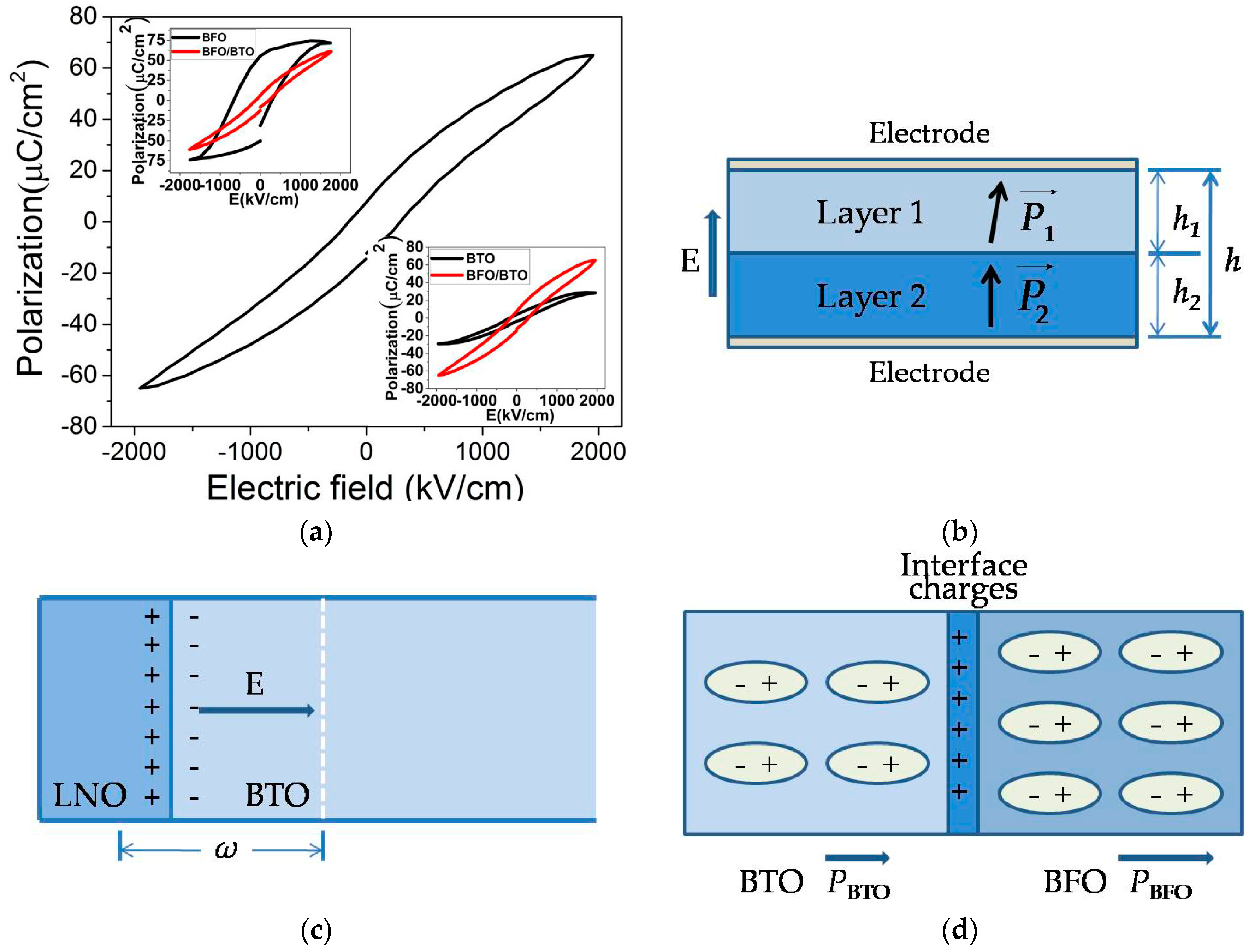
3.2. Energy Storage Characteristics from the P-E Hysteresis Loop

The poling and depoling process of a dielectric under an external electric field simulates the charge-discharge process of a capacitor. Therefore, from the polarization–electric field (P-E) hysteresis loop, the energy storage density Wc and the energy efficiency η of the Au/BiFeO3/BaTiO3/LaNiO3/Pt/Ti capacitors can be calculated by using Equation (1). Figure 4a displays the P-E hysteresis loop measured at a pseudo-static frequency of 1 kHz for the bi-layer film (under an applied electric field of 1940 kV/cm). A large maximum polarization (Pm ~ 65 μC/cm2) and a small remnant polarization (Pr ~ 7.8 μC/cm2) are simultaneously obtained, together with a reduced coercive field Ec (Ec ~ 152 kV/cm) as compared with that of pure BiFeO3 film [22]. These features of the P-E curve ensure excellent energy storage characteristics of the film. When compared with pure BaTiO3 films deposited under similar conditions [23], the energy storage density Wc of the bi-layer film reached 71 J/cm3 (Emax = 1940 kV/cm), a 100%–110% improvement, while the energy efficiency η stayed about the same level (~61% vs. 60%–70%). This improvement in Wc can be attributed to a much improved maximum polarization and a high dielectric strength in par with that of a pure BaTiO3 film.
The “slim-down”of the P-E loop can be explained by the competition between the space charge effect and interlayer charge coupling in the bi-layer film. As demonstrated in our previous study, a space charge layer in BaTiO3 near its interface with LaNiO3 dominates the film’s electrical characteristics at a low electric field [24]. Basically, a depletion region with width ω forms at the BaTiO3/LaNiO3 interface upon the application of a small electric field. The width ω can be computed by [24]:
w = 2 ε ( V + V b i * ) q N e f f ,
where V b i * is the modified built-in voltage, ε is the dielectric constant (ε = ε0εr), Neff is the space charge concentration, V is the applied electric voltage and q the electronic charge. The voltage V is concentrated across the depletion region and drives its expansion until the BaTiO3 layer has been fully depleted. It has been shown that the existence and evolution of a depletion layer in a ferroelectric film will cause shrinking and tilting of its P-E loop, leading to reduced Pr and Ec [25]. On the other hand, after the BaTiO3 layer has been completely depleted, a substantial amount of bound charges appear at the BiFeO3/BaTiO3 interface owing to the large difference in polarizations between the two layers. Hence the charge transport of the bi-layer film under a high electric field will be dominated by the interface charge coupling, which can be described by an added energy term 1 2 ε 0 α(1 − α)( P 1 P 2 )2 in the Landau-Ginzburg-Devonshire (LGD) thermodynamic potential (free energy density F) of the bilayer thick film [26]:
F = ( 1 - α ) [ F 1 ( P 1 ) E P 1 ] + α [ F 2 ( P 2 ) E P 2 ] + 1 2 ε 0 α ( 1 α ) ( P 1 P 2 ) 2
here α = h2/h (h = h1 + h2) is the relative thickness of the second layer, F i , P i (i = 1, 2) are the bulk free energy density and polarization of the ith layer, and E is the applied electric field (see Figure 4b). The third term of the free energy density with the coefficient α(1 − α) expresses the energy of electrostatic interaction between the two layers, and it becomes dominant when the field is large enough to allow both layers become fully poled. In this case, the difference between the two polarizations diminishes and the film shows an “average” polarization. In our case, the polarization of the fully poled bi-layer film Pbi is close to that of BiFeO3 due to the fact that PBFO >> PBTO. The computed Pbi by solving the equilibrium state of Equation (4) is close to 50 μC/cm2 [21], fairly consistent with the observed Pm value if the linear contribution from dielectric susceptibility to the total polarization is deducted. Therefore, the enhanced energy storage capability of the BiFeO3/BaTiO3 bi-layer film can be attributed to a combination of space charge effect (dominant at low field, leading to small Pr and Ec) and effect of interlayer charge coupling (dominant at high field, leading to a large Pm).
Figure 5 a shows the leakage current density versus electric field (J-E) curve. At an electric field of 100 kV/cm (bias voltage of 10 V), the leakage current density of the bi-layer film is 5.0 × 10⁻⁶ A/cm2. This is about an order of magnitude lower than those reported for single layer BiFeO3 films grown on Si substrates [27,28]. The reduction in leakage current is in good agreement with the observed morphology change shown in AFM and SEM images, i.e., a densely and smoothly grown BiFeO3 film was endowed with a much improved electrical resistivity [29]. In addition, an interface energy barrier φB between the BiFeO3 (work function W ~ 4.7 eV) and BaTiO3 (W ~ 4.0 eV) layers can also reduce the leakage current and hence allow the film to be exposed to a large electric field [30,31]. As a result, a high energy density is achieved in the BiFeO3/BaTiO3 bi-layer film.
Figure 5b displays frequency-dependent relative dielectric constant εr and loss tangent tanδ of the bi-layer film. It can be seen that the pseudo static εr is about 425 (@1 kHz), which is about 33% and 70% higher than those of the single layer BaTiO3 and BFO films grown on Si, respectively (εr ~ 320 for BTO, εr ~ 250 for BFO) [22,32]. When the frequency increases from 1 kHz to 1 MHz, εr decreases from ~425 to ~380. On the other hand, tan δ varies between 2.4% and 8.4% in the same frequency range, similar to that of pure BTO films grown on Si. The enhanced dielectric constant εr contributes to the improved maximum polarization Pm, based on the relation Pm = Dm = P + εr × Emax, where P is the self-polarization and PPr for ferroelectrics.

4. Conclusions

In this study, BiFeO3/BaTiO3 bi-layer thick films deposited on the LaNiO3 -buffered Pt/Ti/SiO2/(100) Si substrates display an enhanced energy density and charge-discharge efficiency (Wc = 71 J/cm3, η = 61%) as compared with those of the single layer films. This enhancement can be attributed to combined effects of space charges and the interlayer charge coupling. The bi-layer film exhibits a low leakage current density (5.0 × 10⁻⁶ A/cm2 at 100 kV/cm) as a result of the dense and smooth film morphology achieved in the BFO layer, which is induced by the high quality underlayer of BaTiO3/LaNiO3. The relative dielectric constant εr is about 33% higher than that of the pure BaTiO3 film and 70% higher than that of the pure BFO film. In conclusion, the BiFeO3/BaTiO3 bi-layer film shows excellent dielectric performance and energy storage characteristics, making this structure a promising candidate for applications in microelectronics as lead-free thin film ceramic capacitors.

Acknowledgments

The authors acknowledge the financial support of the Program for New Century Excellent Talents in University (State Education Ministry), Nano Projects of Soochow City (Grant No. ZXG201445), the Fundamental Research Funds of Shandong University (Grant No. 2015JC034, 2015YQ009). J.O. would also like to thank the “Qi-Lu Young Scholar Fund” of Shandong University and the support from the Material Measurement Laboratory of NIST, Gaithersburg, MD (USA).

Conflicts of Interest

The authors declare no conflict of interest.

Notes

For a ferroelectric, its P-E curve is close to D-E curve and the two notations (P-E, D-E) are often interchangeably used for one another. Rigorously, what is measured in a polarization-electric field test (P-E test) of a ferroelectric material is its D-E curve.

References

  1. Wang, Y.; Zhou, X.; Chen, Q.; Chu, B.; Zhang, Q. Recent development of high energy density polymers for dielectric capacitors. IEEE Trans. Dielectr. Electr. Insul. 2010, 17, 1036–1042. [Google Scholar] [CrossRef]
  2. Hao, X.; Wang, Y.; Yang, J.; An, S.; Xu, J. High energy-storage performance in Pb0.91La0.09(Ti0.65Zr0.35) O3 relaxor ferroelectric thin films. J. Appl. Phys. 2012, 112, 114111. [Google Scholar] [CrossRef]
  3. Hao, X.; Wang, Y.; Zhang, L.; Zhang, L.; An, S. Composition-dependent dielectric and energy-storage properties of (Pb,La)(Zr,Sn,Ti) O3 antiferroelectric thick films. Appl. Phys. Lett. 2013, 102, 163903. [Google Scholar] [CrossRef]
  4. Zhang, L.; Hao, X.; Zhang, L. Enhanced energy-storage performances of Bi2O3–Li2O added (1 − x)(Na0.5Bi0.5) TiO3xBaTiO3 thick films. Ceram. Int. 2014, 40, 8847–8851. [Google Scholar] [CrossRef]
  5. Xie, Z.; Yue, Z.; Ruehl, G.; Peng, B.; Zhang, J.; Yu, Q.; Zhang, X.; Li, L. Bi(Ni1/2Zr1/2)O3-PbTiO3 relaxor-ferroelectric films for piezoelectric energy harvesting and electrostatic storage. Appl. Phys. Lett. 2014, 104, 243902. [Google Scholar] [CrossRef]
  6. Xie, Z.; Peng, B.; Meng, S.; Zhou, Y.; Yue, Z. High–Energy-Storage Density Capacitors of Bi (Ni1/2Ti1/2) O3–PbTiO3 Thin Films with Good Temperature Stability. J. Am. Ceram. Soc. 2013, 96, 2061–2064. [Google Scholar] [CrossRef]
  7. Xie, Z.; Peng, B.; Zhang, J.; Zhang, X.; Yue, Z.; Li, L.; Trolier-McKinstry, S.E. Highly (100)-Oriented Bi(Ni1/2Hf1/2)O3-PbTiO3Relaxor-Ferroelectric Films for Integrated Piezoelectric Energy Harvesting and Storage System. J. Am. Ceram. Soc. 2015, 98, 2968–2971. [Google Scholar] [CrossRef]
  8. Xie, Z.; Yue, Z.; Peng, B.; Zhang, J.; Zhao, C.; Zhang, X.; Ruehl, G.; Li, L. Large enhancement of the recoverable energy storage density and piezoelectric response in relaxor-ferroelectric capacitors by utilizing the seeding layers engineering. Appl. Phys. Lett. 2015, 106, 202901. [Google Scholar] [CrossRef]
  9. Xie, Z.; Peng, B.; Zhang, J.; Zhang, X.; Yue, Z.; Li, L. Effects of thermal anneal temperature on electrical properties and energy-storage density of Bi(Ni1/2Ti1/2)O3–PbTiO3 thin films. Ceram. Int. 2015, 41, 206–212. [Google Scholar] [CrossRef]
  10. Lee, B.D.; Lee, H.R.; Yoon, K.H.; Cho, Y.S. Microwave dielectric properties of magnesium calcium titanate thin films. Ceram. Int. 2005, 31, 143–146. [Google Scholar] [CrossRef]
  11. Huang, C.L.; Chen, Y.B. Structure and electrical characteristics of RF magnetron sputtered MgTiO3. Surf. Coat. Technol. 2006, 200, 3319–3325. [Google Scholar] [CrossRef]
  12. Tkach, A.; Almeida, A.; Moreira, J.A.; Perez de la Cruz, J.; Romaguera-Barcelay, Y.; Vilarinho, P.M. Low-temperature dielectric response of NaTaO3 ceramics and films. Appl. Phys. Lett. 2012, 100, 192909. [Google Scholar] [CrossRef]
  13. Liu, G.Z.; Wang, C.; Wang, C.C.; Qiu, J.; He, M.; Xing, J.; Jin, K.J.; Lu, H.B.; Yang, G.Z. Effects of interfacial polarization on the dielectric properties of BiFeO3 thin film capacitors. Appl. Phys. Lett. 2008, 92, 122903. [Google Scholar] [CrossRef]
  14. Lee, S.J.; Kang, K.Y.; Kim, J.W.; Han, S.K.; Jeong, S.D. Low-Frequency Dielectric Properties of Sol-Gel Derived BaTiO3 Thin Films. In Proceedings of the Materials Research Society, Nashville, TN, USA, 28 September–1 October 2011.
  15. Yuan, M.; Zhang, W.; Wang, X.; Pan, W.; Wang, L.; Ouyang, J. In situ preparation of high dielectric constant, low-loss ferroelectric BaTiO3 films on Si at 500 °C. Appl. Surf. Sci. 2013, 270, 319–323. [Google Scholar] [CrossRef]
  16. Zhu, H.; Sun, X.; Kang, L.; Zhang, Y.; Yu, Z.; Ouyang, J.; Pan, W. Microstructural and electrical characteristics of epitaxial BiFeO3 thick films sputtered at different Ar/O2 flow ratios. CrystEngComm 2016, 18, 4604–4612. [Google Scholar] [CrossRef]
  17. Gao, Y.; Yuan, M.; Sun, X.; Ouyang, J. In situ preparation of high quality BaTiO3 dielectric films on Si at 350–500 °C. J. Mater. Sci. Mater. Electron. 2016. [Google Scholar] [CrossRef]
  18. Lee, C.C.; Wu, J.M. Effect of film thickness on interface and electric properties of BiFeO3 thin films. Appl. Surf. Sci. 2007, 253, 7069–7073. [Google Scholar] [CrossRef]
  19. Yan, F.; Zhu, T.J.; Lai, M.O.; Lu, L. Influence of oxygen pressure on the ferroelectric properties of BiFeO3 thin films on LaNiO3/Si substrates via laser ablation. Appl. Phys. A 2010, 101, 651–654. [Google Scholar] [CrossRef]
  20. Dho, J.; Qi, X.; Kim, H.; MacManus-Driscoll, J.L.; Blamire, M.G. Large Electric Polarization and Exchange Bias in Multiferroic BiFeO3. Adv. Mater. 2006, 18, 1445–1448. [Google Scholar] [CrossRef]
  21. Zhu, H.; Liu, M.; Zhang, Y.; Yu, Z.; Ouyang, J.; Pan, W. Increasing energy storage capabilities of space-charge dominated ferroelectric thin films using interlayer coupling. Acta Mater. 2016, 122, 252–258. [Google Scholar] [CrossRef]
  22. Hussain, S.; Hasanain, S.K.; Hassnain Jaffari, G.; Ismat Shah, S. Thickness dependent magnetic and ferroelectric properties of LaNiO3 buffered BiFeO3 thin films. Curr. Appl. Phys. 2015, 15, 194–200. [Google Scholar] [CrossRef]
  23. Yuan, M.L. Medium Temperature Preparation of BaTiO3 Thin Film Capacitors with High Breakdown Voltages and Large Electric Energy Densities. Master’s Thesis, Shandong University, Jinan, China, 2014. [Google Scholar]
  24. Zhang, W.; Gao, Y.; Kang, L.; Yuan, M.; Yang, Q.; Cheng, H.; Pan, W.; Ouyang, J. Space-charge dominated epitaxial BaTiO3 heterostructures. Acta Mater. 2015, 85, 207–215. [Google Scholar] [CrossRef]
  25. Tagantsev, A.K.; Landivar, M.; Colla, E.; Setter, N. Identification of passive layer in ferroelectric thin films from their switching parameters. J. Appl. Phys. 1995, 78, 2623. [Google Scholar] [CrossRef]
  26. Roytburd, A.L.; Zhong, S.; Alpay, S.P. Dielectric anomaly due to electrostatic coupling in ferroelectric-paraelectric bilayers and multilayers. Appl. Phys. Lett. 2005, 87, 092902. [Google Scholar] [CrossRef]
  27. Liu, Y.T.; Ku, C.S.; Chiu, S.J.; Lee, H.Y.; Chen, S.Y. Ultrathin oriented BiFeO3 films from deposition of atomic layers with greatly improved leakage and ferroelectric properties. ACS Appl. Mater. Interfaces 2014, 6, 443–449. [Google Scholar] [CrossRef] [PubMed]
  28. Simões, A.Z.; Riccardi, C.S.; Dos Santos, M.L.; Garcia, F.G.; Longo, E.; Varela, J.A. Effect of annealing atmosphere on phase formation and electrical characteristics of bismuth ferrite thin films. Mater. Res. Bull. 2009, 44, 1747–1752. [Google Scholar] [CrossRef]
  29. Kawae, T.; Terauchi, Y.; Tsuda, H.; Kumeda, M.; Morimoto, A. Improved leakage and ferroelectric properties of Mn and Ti codoped BiFeO3 thin films. Appl. Phys. Lett. 2009, 94, 112904. [Google Scholar] [CrossRef]
  30. Wang, C.; Jin, K.J.; Xu, Z.T.; Wang, L.; Ge, C.; Lu, H.B.; Guo, H.Z.; He, M.; Yang, G.Z. Switchable diode effect and ferroelectric resistive switching in epitaxial BiFeO3 thin films. Appl. Phys. Lett. 2011, 98, 192901. [Google Scholar] [CrossRef]
  31. Sun, S.; Wang, Y.; Fuierer, P.A.; Tuttle, B.A. Annealing effects on the internal bias field in ferroelectric PZT thin films with self-polarization. Integr. Ferroelectr. 1999, 23, 25–43. [Google Scholar] [CrossRef]
  32. Yan, F.; Zhu, T.J.; Lai, M.O.; Lu, L. Effect of bottom electrodes on nanoscale switching characteristics and piezoelectric response in polycrystalline BiFeO3 thin films. J. Appl. Phys. 2011, 110, 084102. [Google Scholar] [CrossRef]
Figure 1. Schematic of a ferroelectric P-E loop. The green area is the discharged energy density Wd, while the yellow area is the energy loss of one charge-discharge cycle (Wloss).
Materials 09 00935 g001
Figure 2. Schematics of the experimental procedures.
Materials 09 00935 g002
Figure 3. (a) XRD 2θ scan spectrum (R-rhombohedral, T- tetragonal for BFO peaks, while the BTO phase is tetragonal); (b) X-ray pole figure analyses by using the (001)R BFO peak; (c) AFM surface scan image (5 μm × 5 μm); and (d) cross-sectional SEM image of the BiFeO3/BaTiO3 bi-layer film deposited on LaNiO3/Pt/Ti/SiO2/(100) Si substrate.
Materials 09 00935 g003
Figure 4. (a) Room temperature ferroelectric hysteresis loop of the BiFeO3/BaTiO3 bi-layer film deposited on LaNiO3/Pt/Ti/SiO2/(100)Si substrate, the insets compare P-E loops of the pure BiFeO3 and BaTiO3 films with those of the bi-layer film measured under the same electric field [22,23]; (b) schematics of the ferroelectric bi-layer considered in our work; (c) the space charge effect dominant at a low electric field, ω is the depletion layer width under an electric field E; (d) strong interlayer charge coupling dominant at a high electric field (after the BaTiO3 layer has been fully depleted).
Materials 09 00935 g004
Figure 5. (a) Leakage current density vs. voltage (J-V) curve; and (b) frequency dependent dielectric properties of the BiFeO3/BaTiO3 bi-layer film.
Materials 09 00935 g005
Table 1. Deposition Parameters of the Sputtering Process for BiFeO3/BaTiO3 Bi-layer Films on SiO2/(100) Si Substrates.
Sputtering ParametersBFOBTOLNO
Sputtering power (W)100
Substrate temperature (°C)500
Sputtering pressure (Pa)1.20.3
Sputtering atmosphere Ar + O2 (4:1 flow ratio)
Cooling atmosphere and pressurePure oxygen, 2.5 Pa
Pt/Ti sputtering parameters300 °C, 0.3 Pa, 55 W, pure Ar

