
Ferroelectrics under the Synchrotron Light: A Review


Abstract
: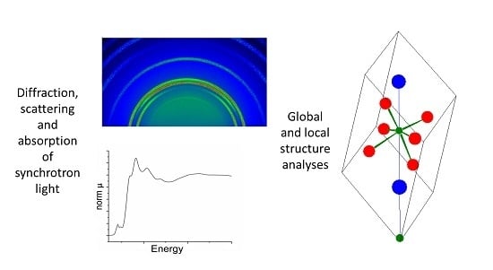
1. Introduction

2. X-ray Diffraction and Scattering
2.1. One-Dimensional Measurements

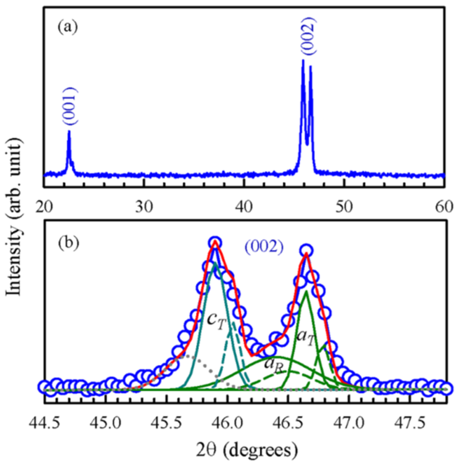
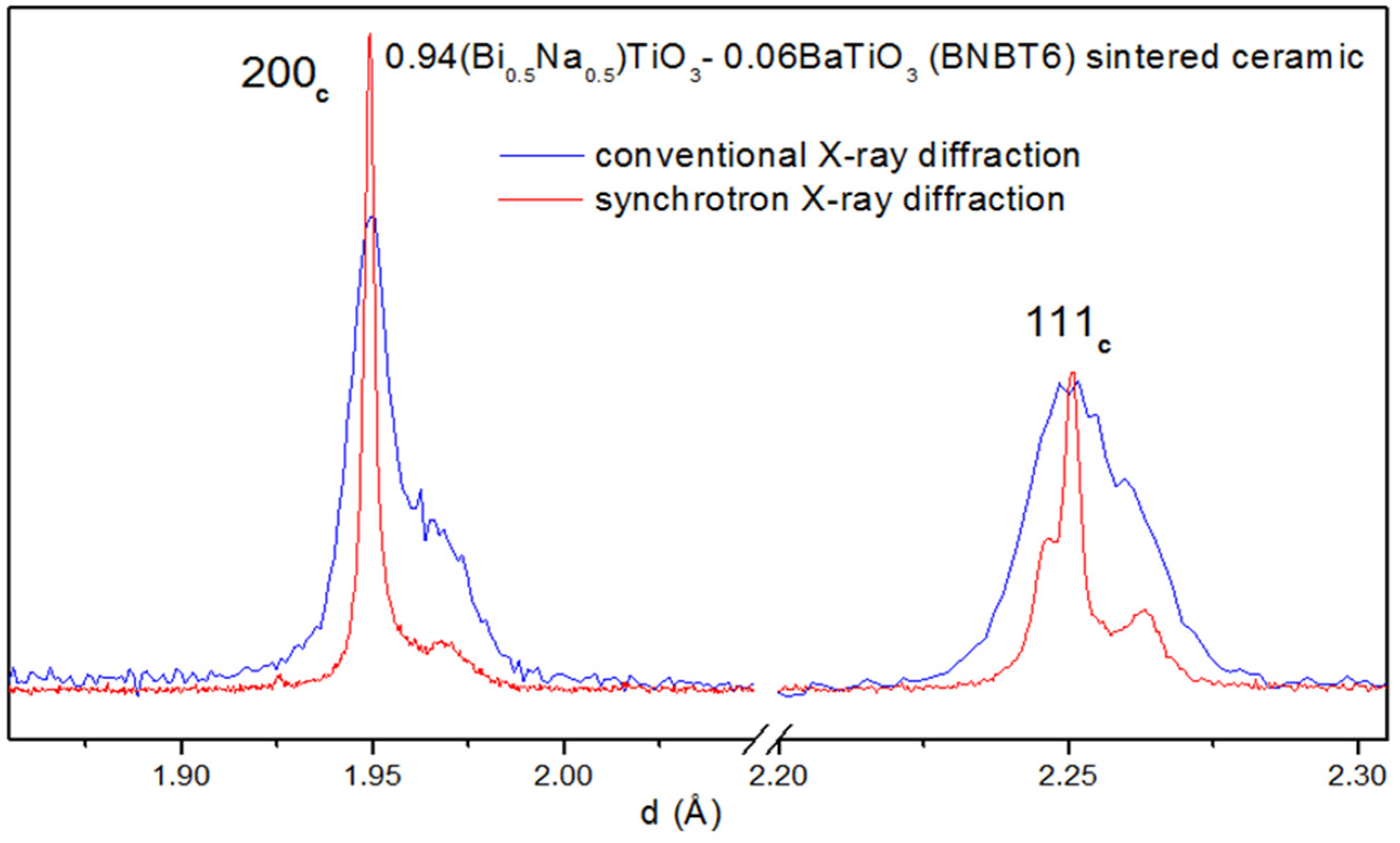
2.1.1. Recent Work on PZT and BaTiO3 [12,32]

2.1.2. Texture
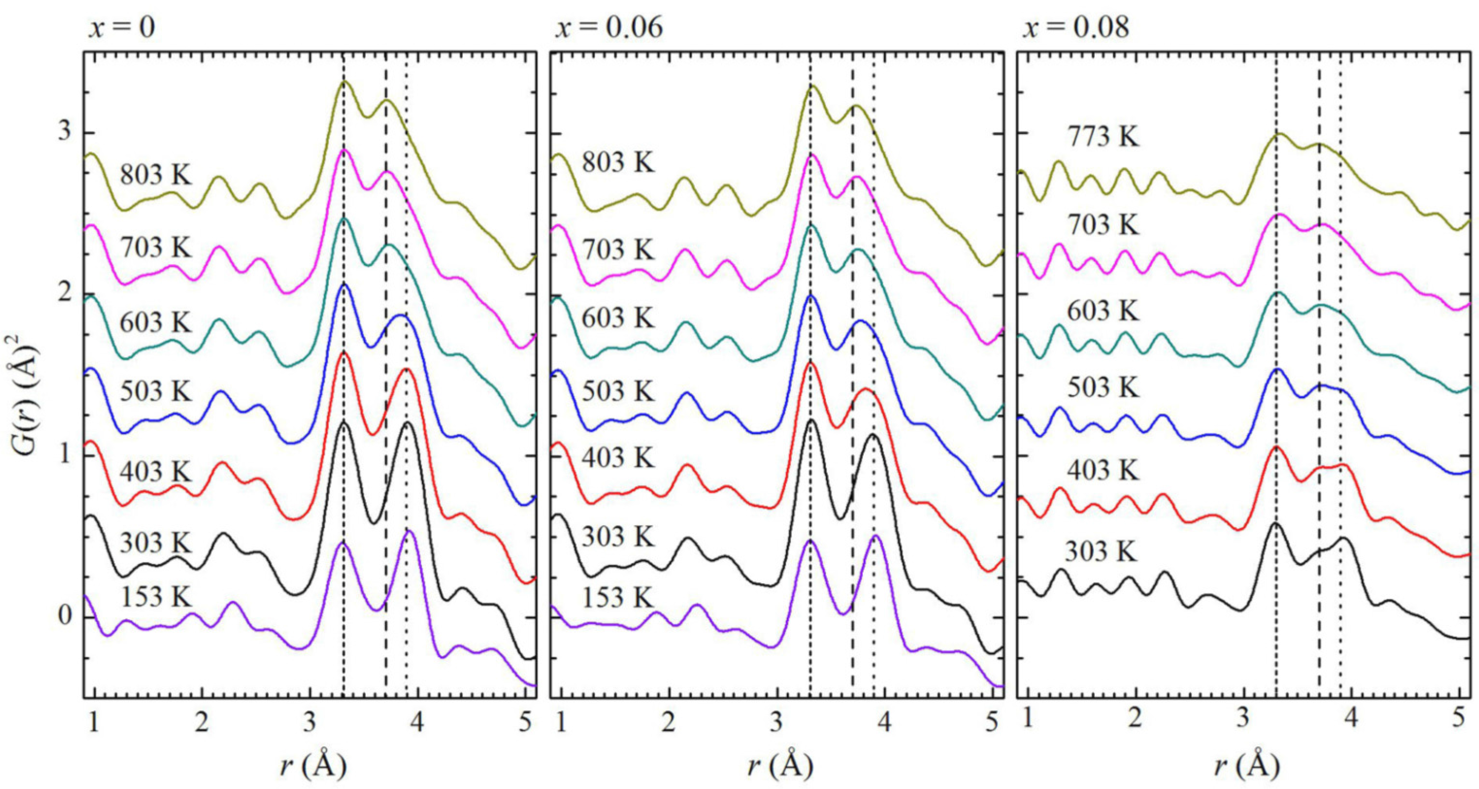
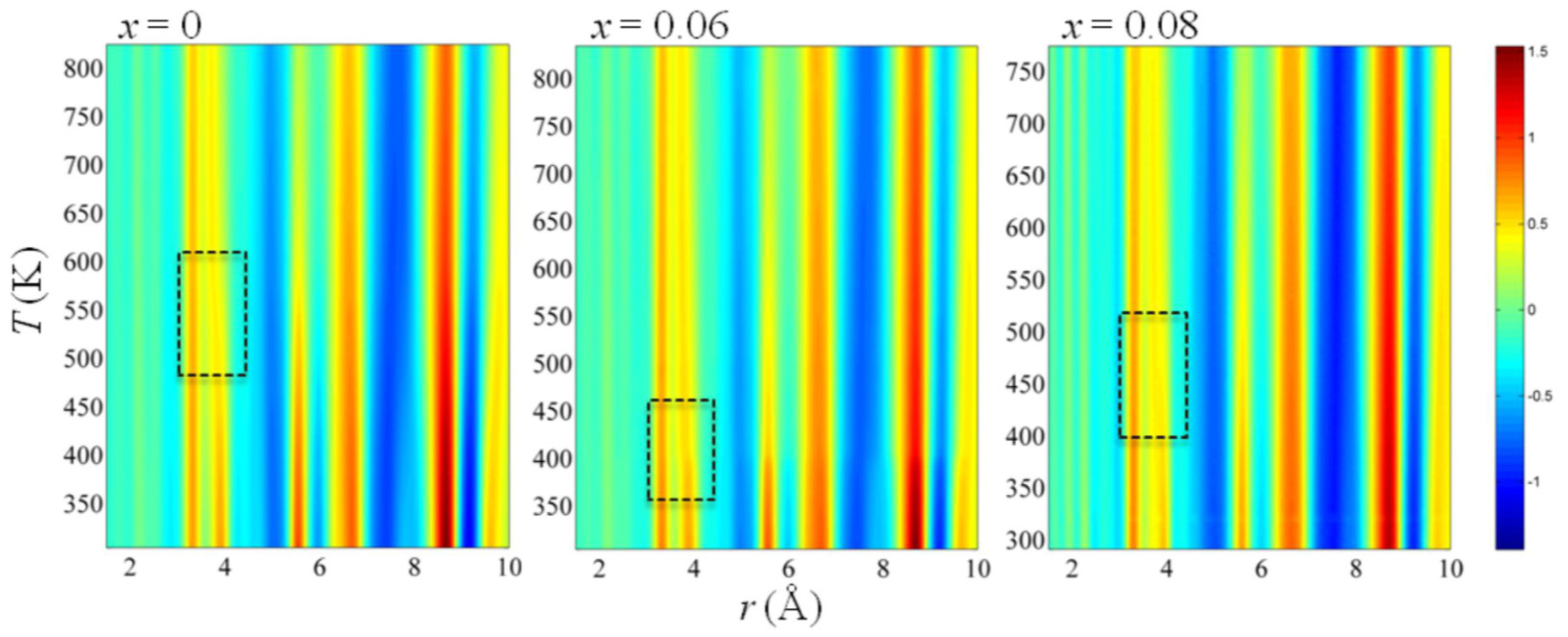
2.1.3. Diffuse Scattering: PDF Analysis


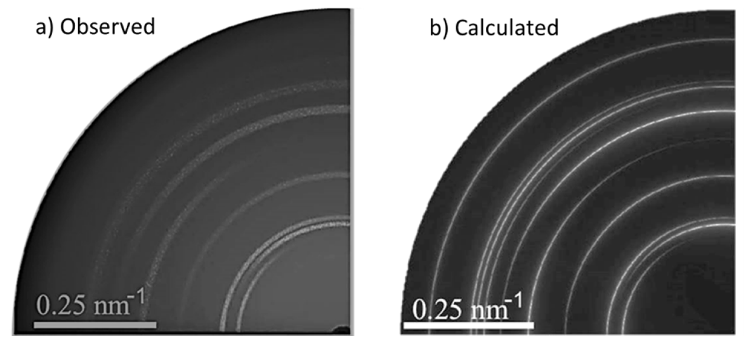
2.2. Two-Dimensional Measurements
2.2.1. Two-Dimensional Image Plate
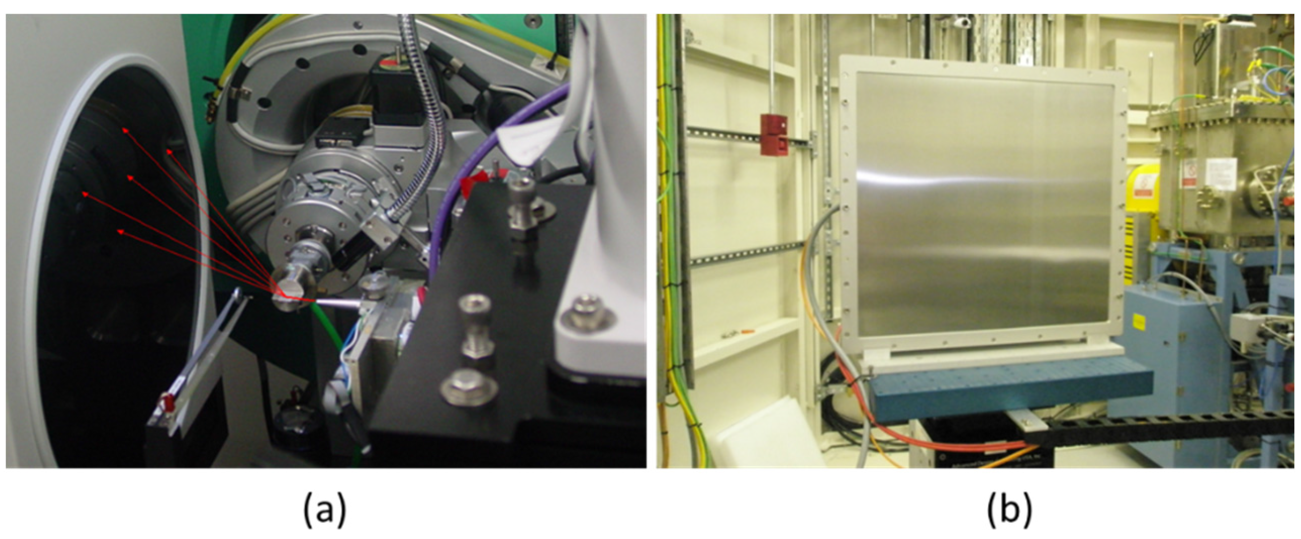
2.2.2. Charge-Coupled Device (CCD)
2.2.3. Single-Photon—Counting Mode
2.2.4. Grazing Incidence 2D-XRD: Texture Analysis
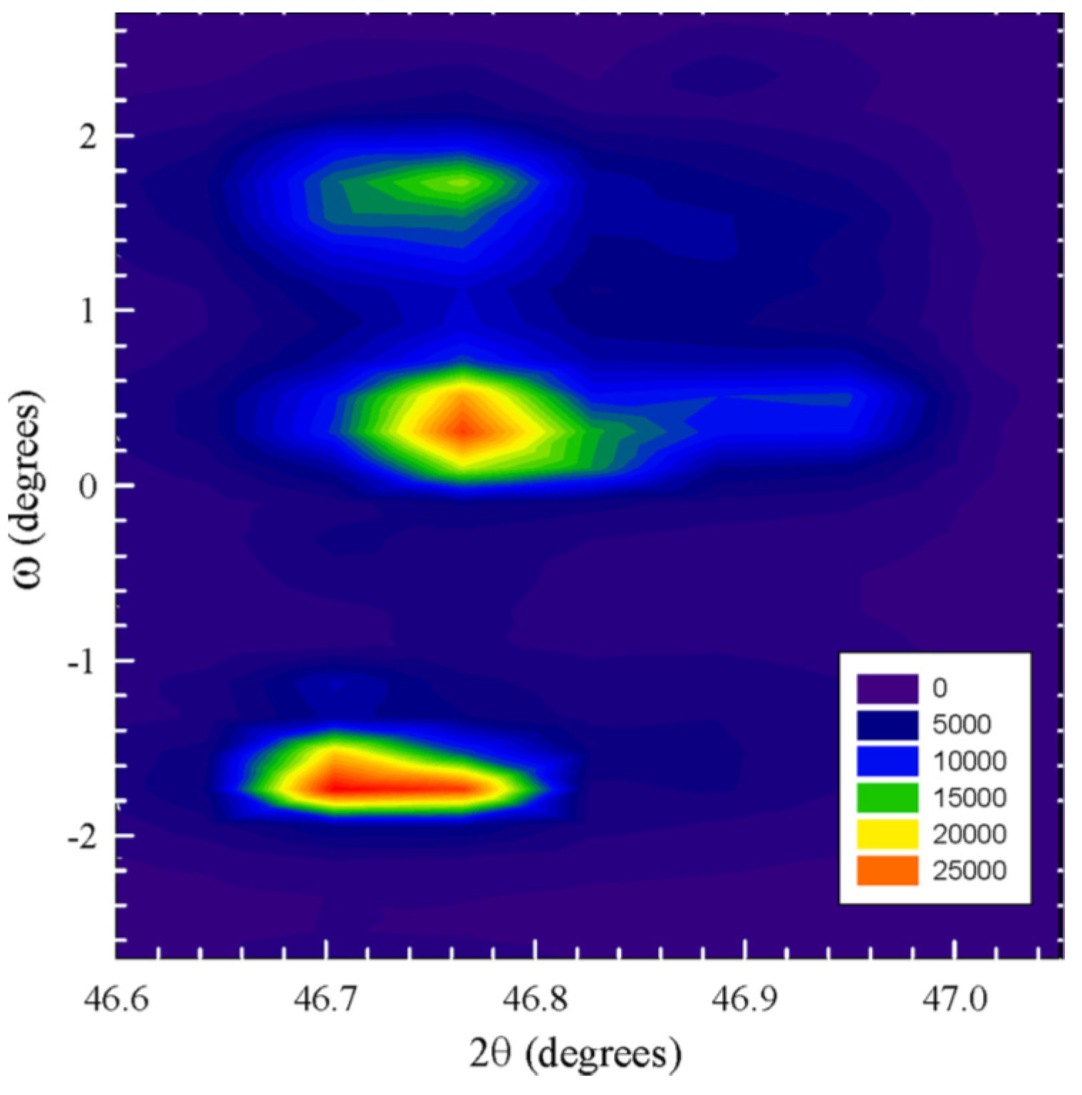
2.2.5. 2D-Diffuse Scattering: Reciprocal Space Mapping

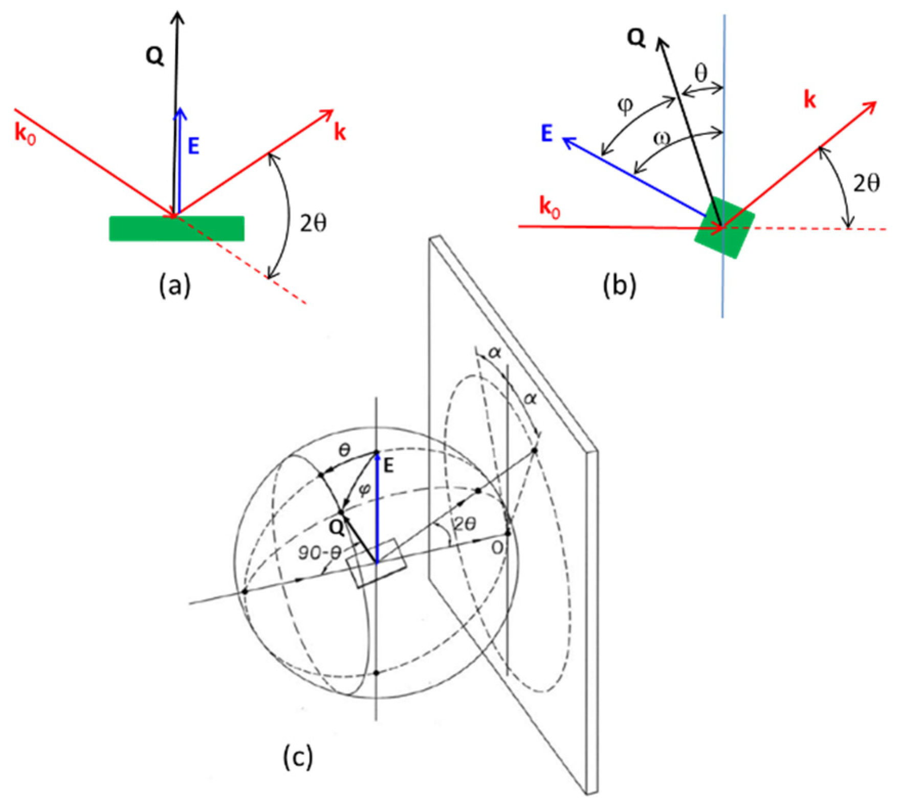
2.3. XRD With In-Situ Applied Electric Field

| Setup (Figure 12) | Reference | Angle between Q and E |
|---|---|---|
| Symmetric reflection (12a) | Present report | 0 |
| [62] | 90° | |
| Asymmetric transmission (12b) | [68] E // k0 | = ω − θ |
| [69] E ⊥ k0 | ||
| 2D-XRD (12c) | [57,58] | cos = cosθ·cosα [54] |
| Synchrotron | Beamline | Energy, Wavelength | Diffraction Geometry | Detector | References |
|---|---|---|---|---|---|
| HASYLAB, DESY. Hamburg, Germany | B2 | 25 keV, 0.5 Å | Transmission with parallel electric field | position-sensitive image-plate | [25,56,68] |
| European Synchrotron Radiation Facility (ESRF). Grenoble, France | ID15B | 87.7 keV, 0.14 Å | Transmission with transverse electric field | 2D detector (Pixium 4700) | [15,37,57,59]. |
| ID11 | 80.5 keV, 0.155 Å | Transmission with transverse electric field or mechanical loads | FReLoN4M area detector | [26,60,64,65] | |
| BM28-XMaS | 9.8 keV, 1,26 Å | Electric field applied parallel to the explored surface | MAR CCD camera | [62] | |
| Elettra Sincrotrone, Trieste, Italy | MCX | 13 keV, 0.95 Å | 4-circle Huber goniometer | 2D detector, MAR345 | [70] |
| Swiss Light Source (SLS). Villigen, Switzerland | MS - X04SA: Materials Science | 28 keV 0.443Å | static field in the beam direction | solid-state silicon microstrip, MYTHEN detector | [61] |
| Advanced Photon Source at Argonne Nat. Lab. Lemont, IL, USA | 5-BM-D | 65 keV 0.1907 Å | Transmission with transverse electric field | 2D detector, MAR345 | [63] |
| Synchrotron Radiation Research Institute (SPring-8). Japan | BL02B1 | 35 keV 0.35 Å | Transmission, three-axis goniometer for single-crystal orientation | large cylindrical two-dimensional imaging plate (IP) camera | [66,67] |
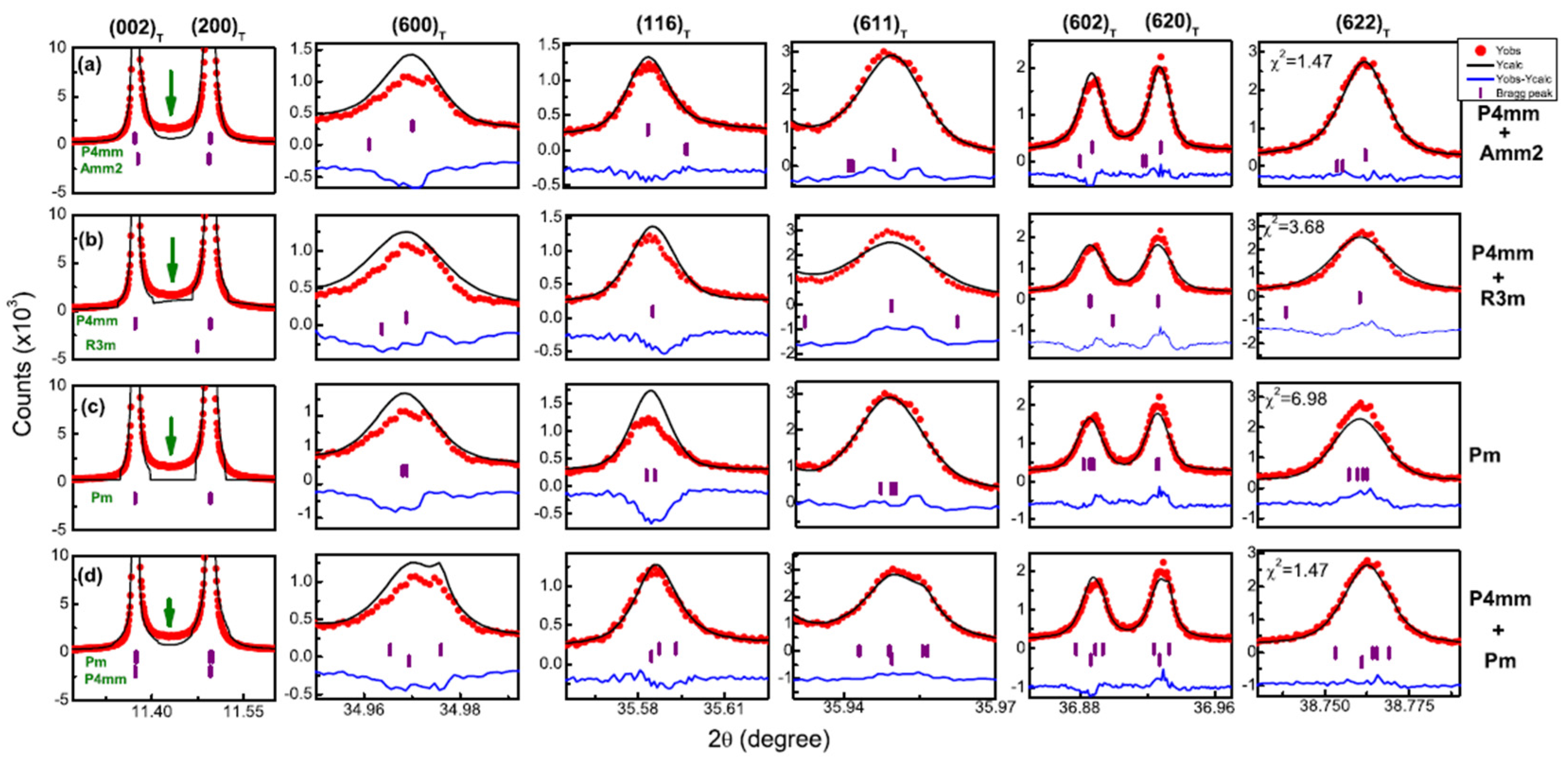
Rietveld Analysis of Structures under an Applied Electric Field
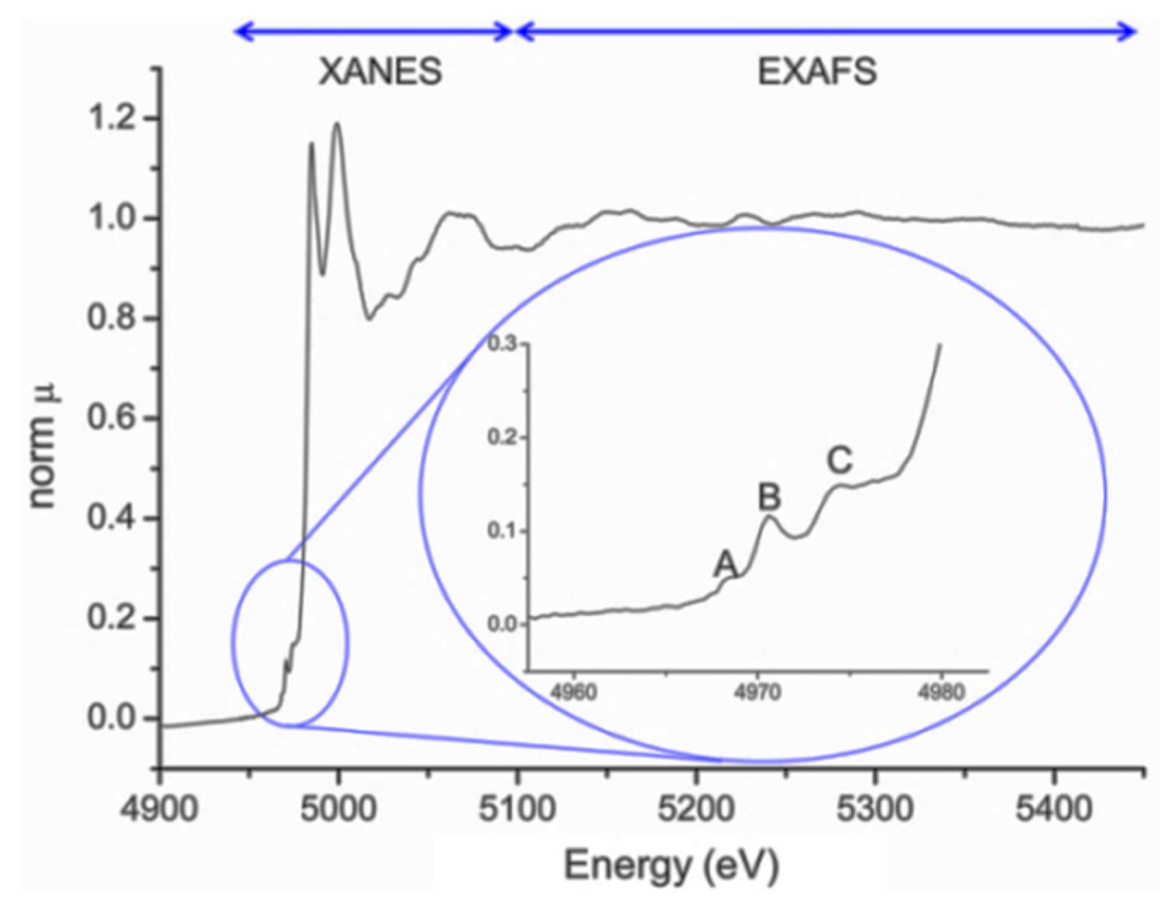
3. X-ray Absorption Fine Structure Spectroscopy
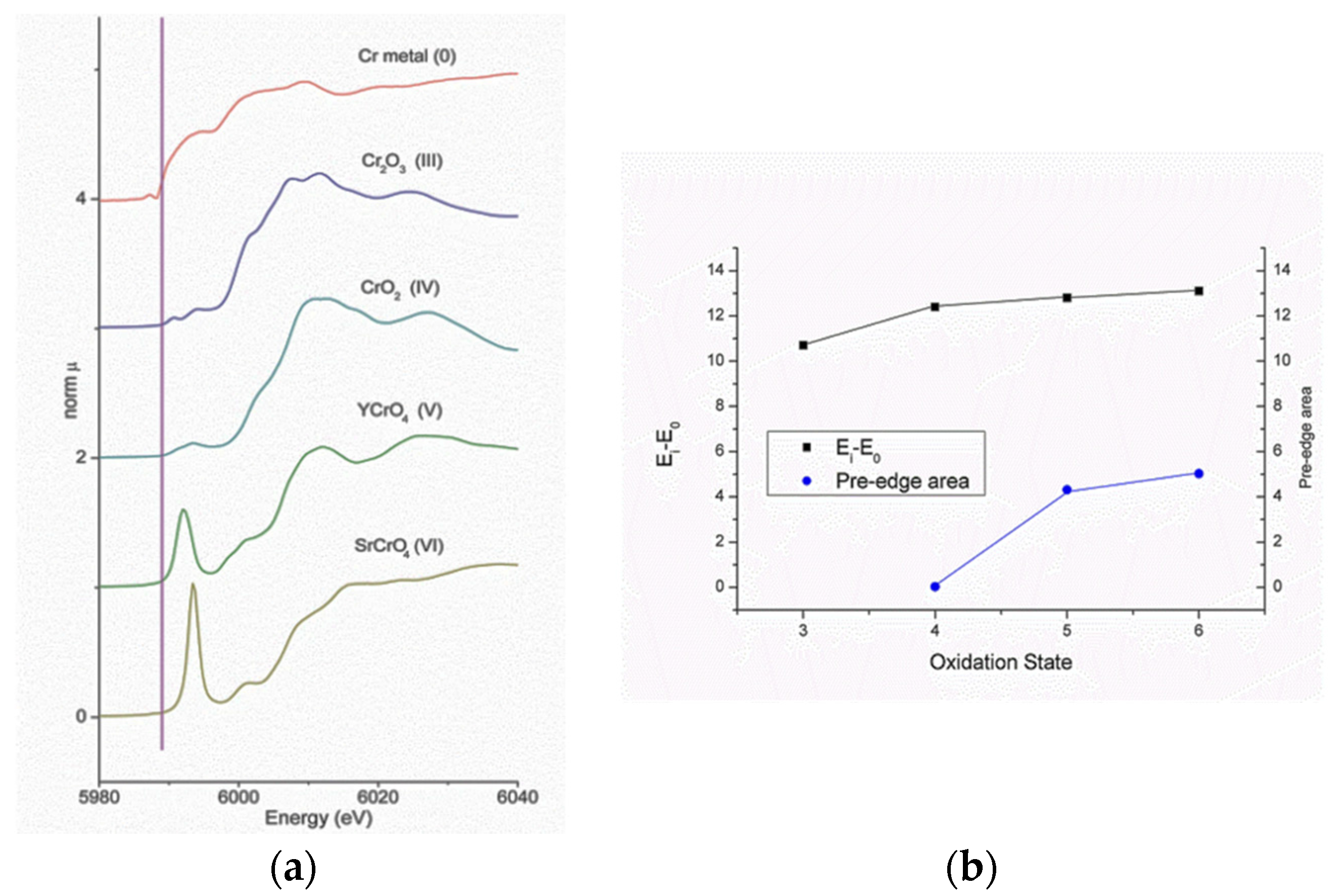
3.1. General


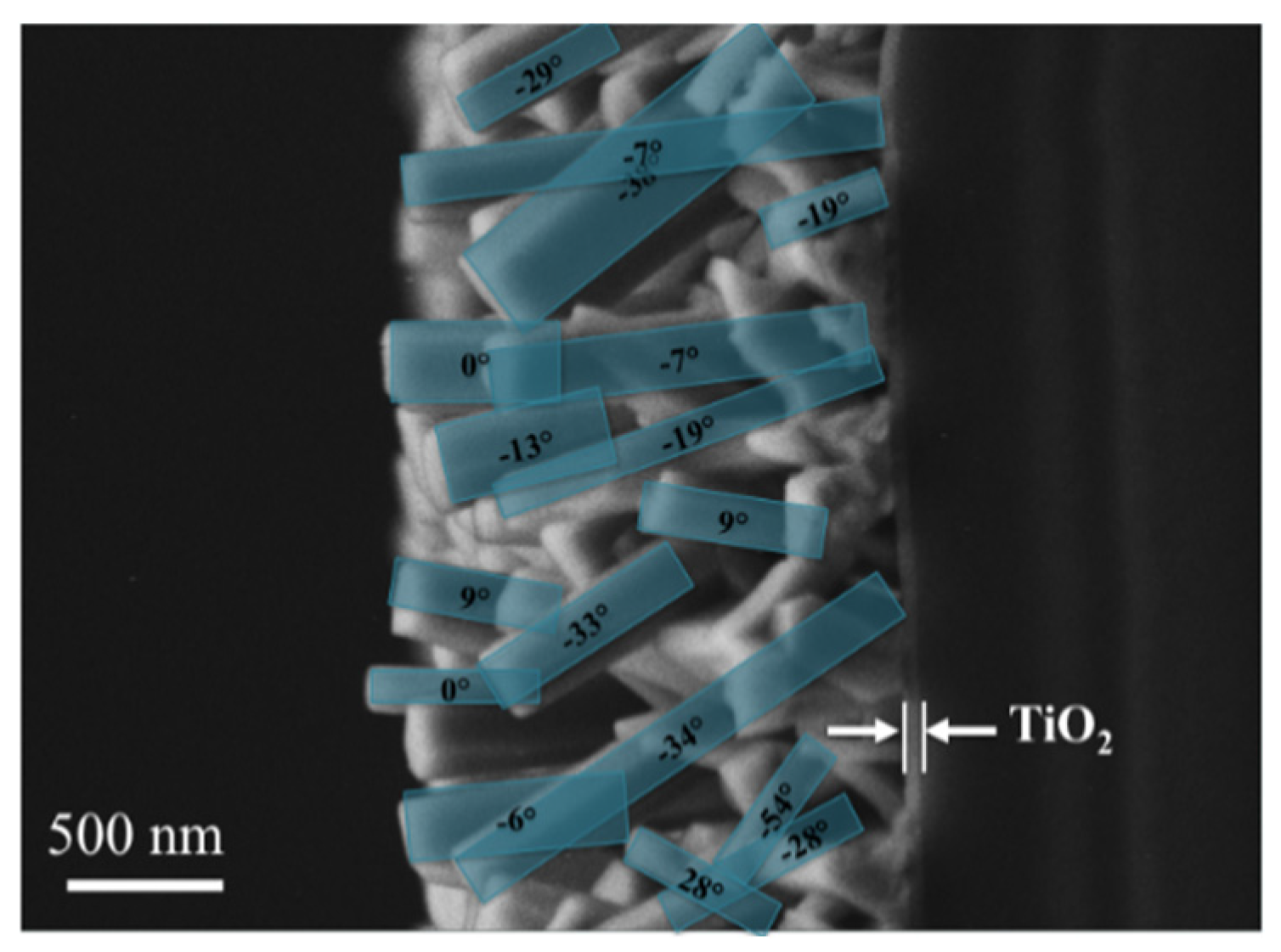
3.2. PbTiO3-Based Ceramics Studied by XAFS
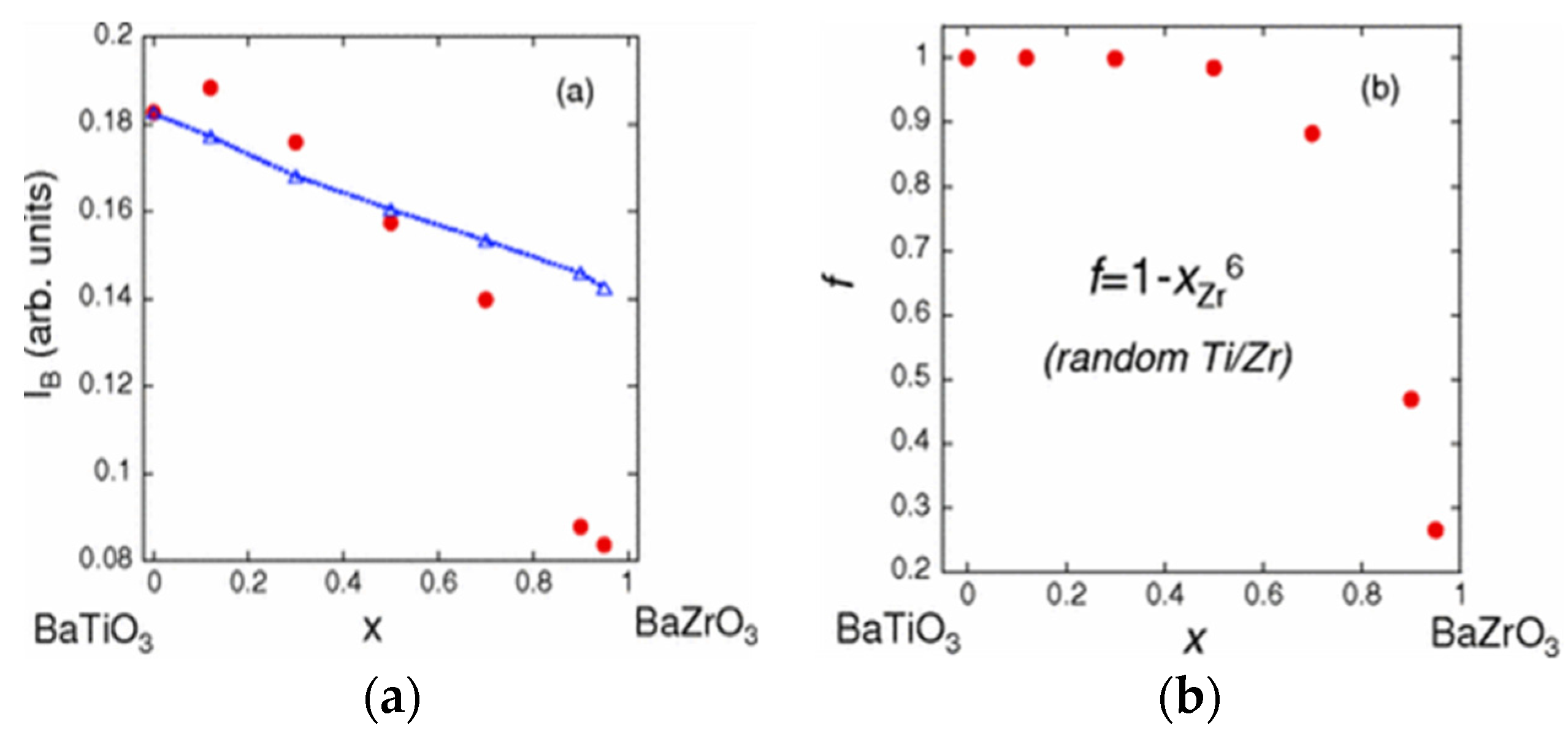
3.3. BaTiO3-Based Ceramics Studied by XAFS
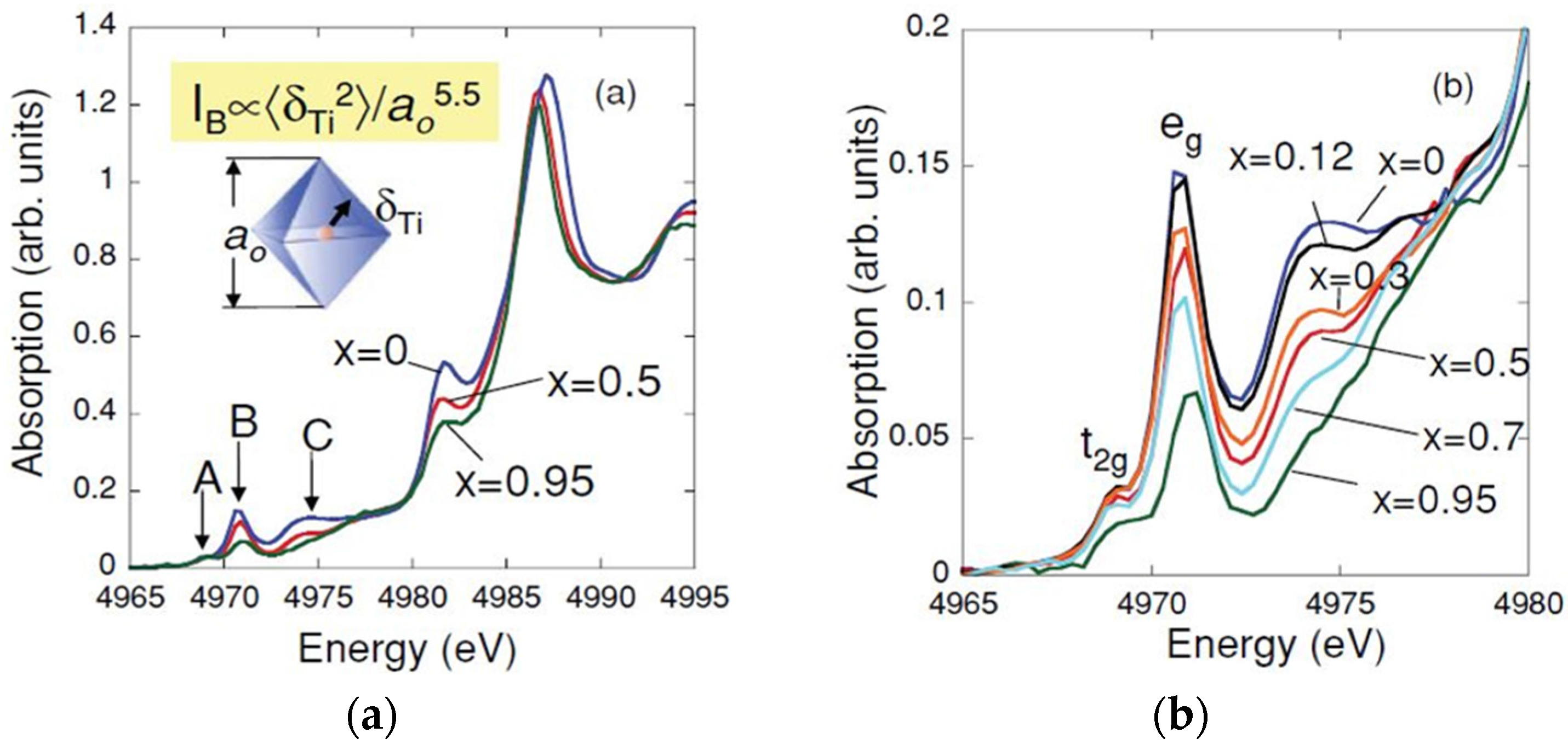

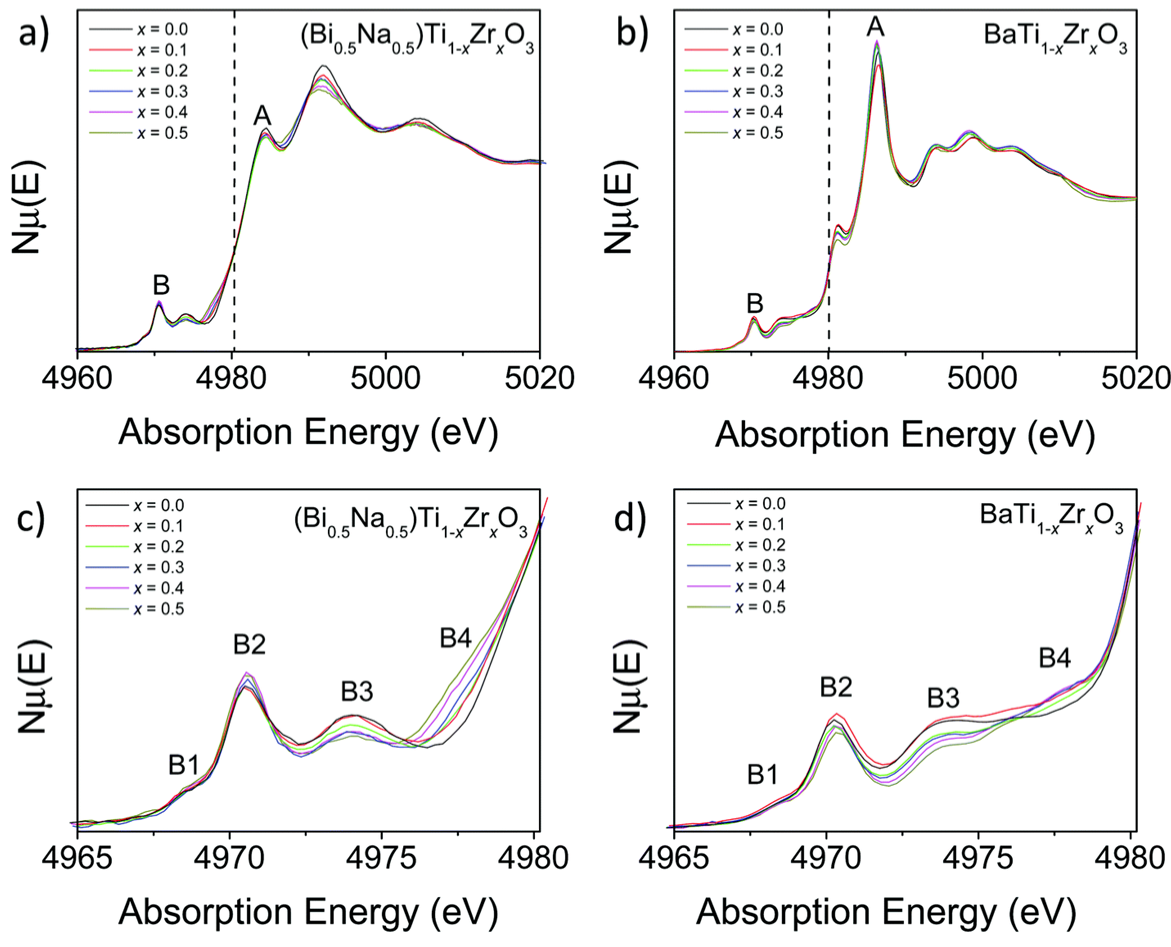
3.4. The (Bi0.5Na0.5)TiO3 Family Studied by XAFS

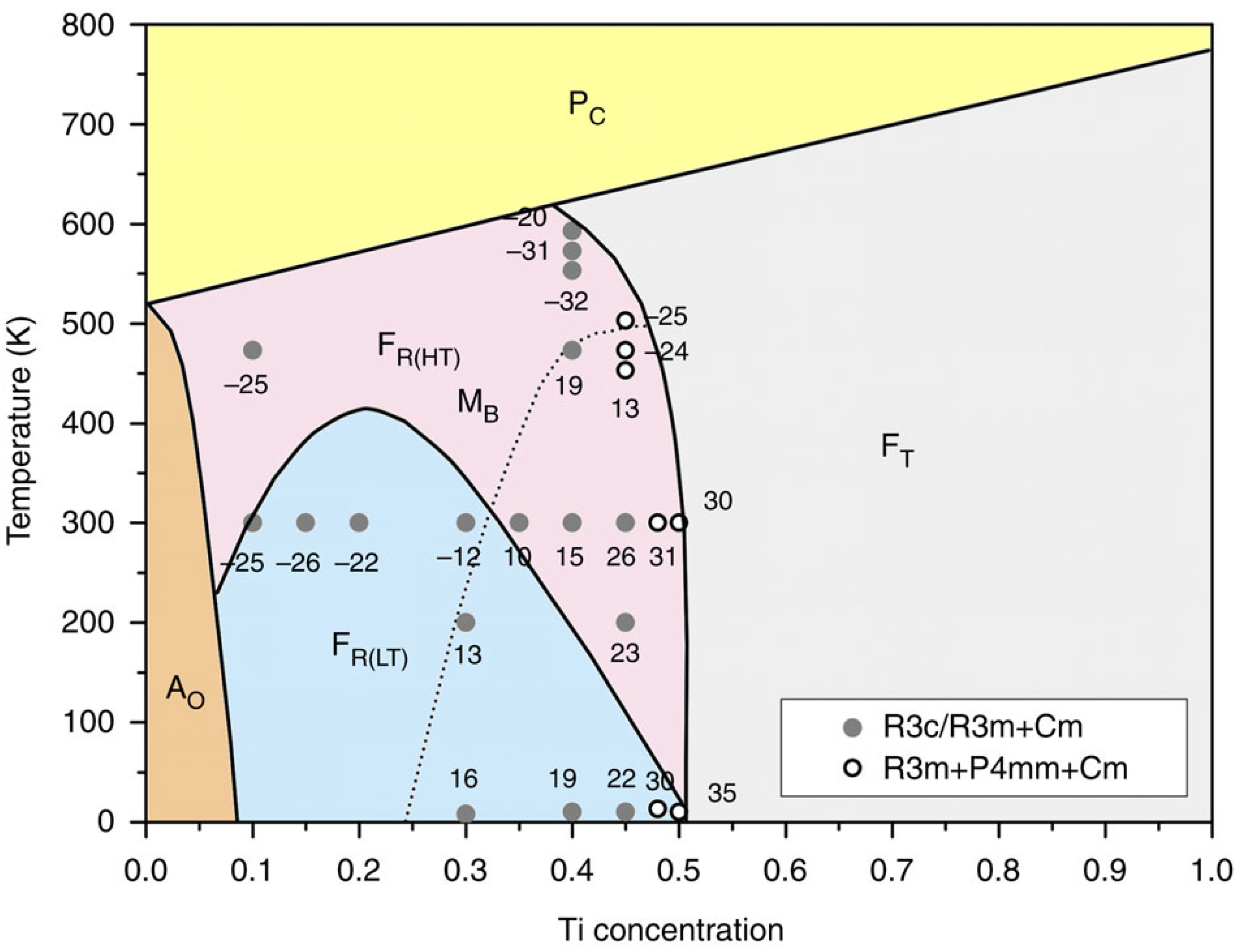
4. Case Study: The BNBT System
4.1. Introduction

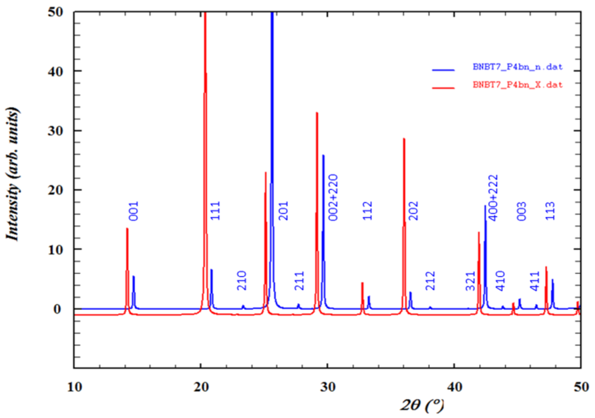
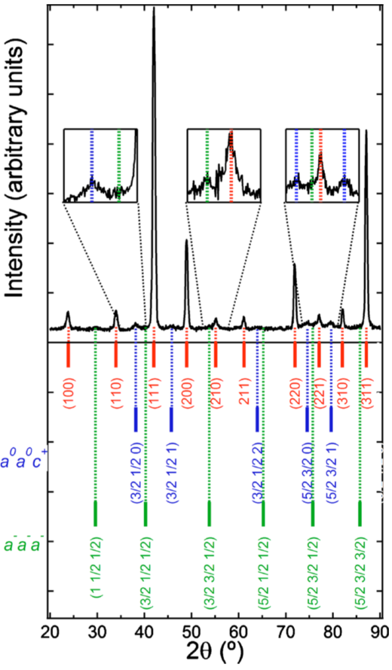
4.2. Diffraction


4.3. XAFS
| Sample | 〈IB〉 (eV) | 〈δ2〉 (A2) | K (eV A3.5) |
|---|---|---|---|
| PbTiO3 | 1.0 (2) | 0.308 (4) a | 6.5 (1)·104 |
| BNBT4-powder | 0.95 (9) | – | – |
| BNBT4-ceramic | 0.86 (8) | – | – |
| BNBT6-powder | 1.02 (9) | 0.069 (6) b | 1.1 (2)·106 |
| BNBT6-ceramic | 0.8 (1) | – | – |
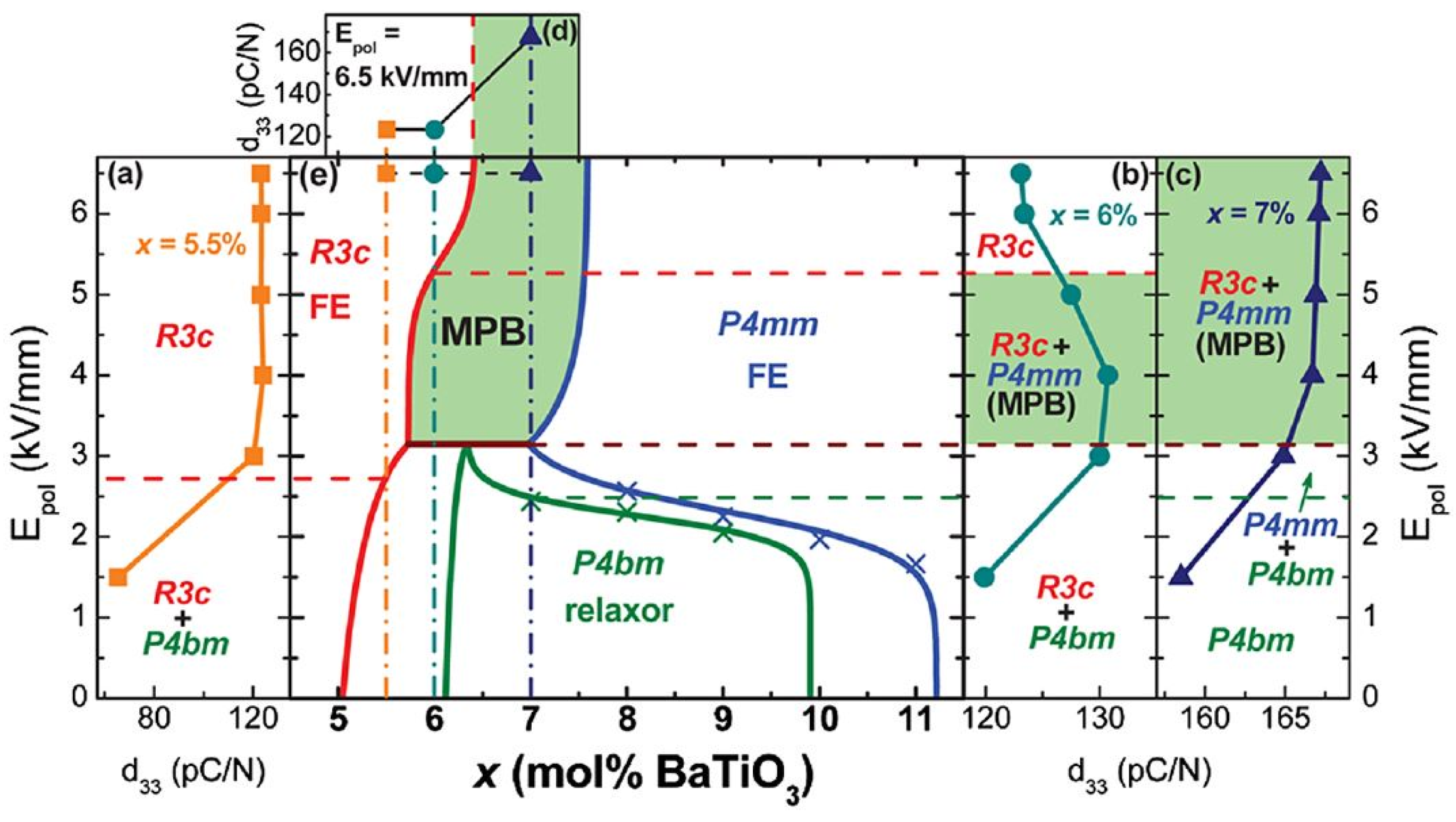
4.4. BNBT MPB Summary
- BNBT4 is essentially R3c + NTL;
- Unpoled BNBT6 contains R3c and pseudocubic global phase + NTL;
- Unpoled BNBT7 contains pseudocubic global phase + NTL;
- So-called pseudocubic phase consists of P4bm 3D nanodomains embedded in a cubic matrix;
- Under poling, BNBT6 shows R3c symmetry and BNBT7 becomes predominantly P4mm;
| Material | Structure/Symmetry | a (Å) | c (Å) | Source | ||
|---|---|---|---|---|---|---|
| BNBT4 unpoled | R3c + NTL | 5.4966(2) | 13.5290(6) | [70] | ||
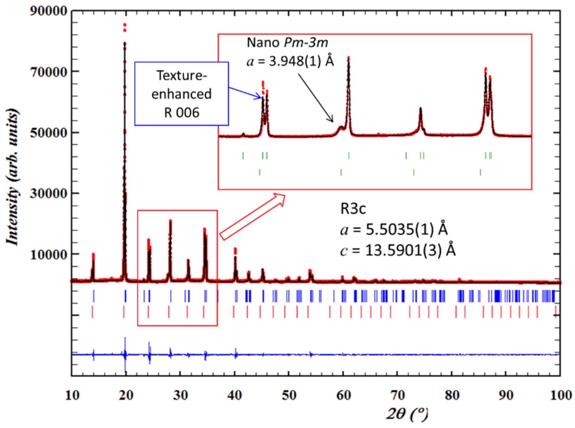
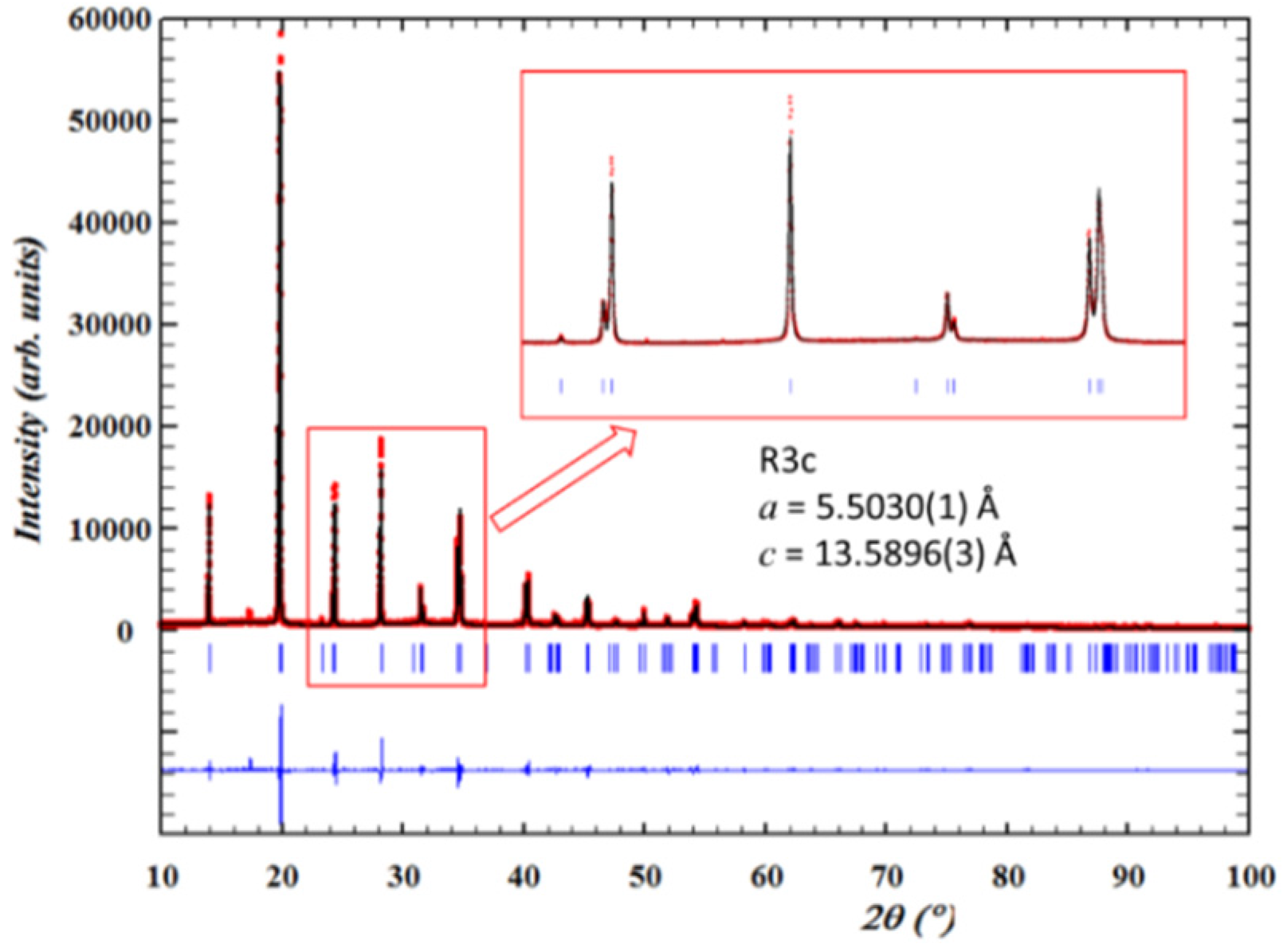
| BNBT6 | Unpoled | R3c | 5.505(1) | 13.598(1) | [87] | |
| P4bm relaxor + NTL | ≅5.5172 | ≅3.9010 | ||||
| Poled | Ceramic | R3c + NTL | 5.5035(1) | 13.5901(3) | Present report | |
| Milled | R3c | 5.5030(1) | 13.5896(3) | |||
| BNBT7 unpoled | P4bm relaxor + NTL | 5.5229(1) | 3.9063(1) | [111] | ||
| Material | Atom | Wyck | x | y | z | SOF | ITF (B) | Source |
|---|---|---|---|---|---|---|---|---|
| BNBT4 R3c unpoled | Bi, Na, Ba | 6a | 0 | 0 | 0.250 | 0.48 | Anisotropic factors given in [70] | [70] |
| Ti | 6a | 0 | 0 | −0.0043(1) | 0.04 | |||
| O | 18b | 0.1307(1) | 0.3404(1) | 0.0843(1) | 1 | |||
| BNBT6 R3c poled, milled | Bi, Na, Ba | 6a | 0 | 0 | 0.250 | 0.47 | 2.88(3) | Present report |
| Ti | 6a | 0 | 0 | −0.0050(4) | 0.06 | 1.92(6) | ||
| O | 18b | 0.146(1) | 0.355(1) | 0.0593(4) | 1 | 2.7(2) | ||
| BNBT7 P4bm unpoled | Bi, Na, Ba | 2b | 0 | 0.5 | 0.553(2) | 0.465 | Anisotropic factors given in [111] | [111] |
| Ti | 2a | 0 | 0 | 0 | 0.07 | |||
| O | 2a | 0 | 0 | 0.512(1) | 1 | |||
| O | 4c | 0.263(1) | 0.237(1) | 0.030(1) | 1 |
5. General Summary
| Techniques | Revealed structural features | ||
| Diffraction/scattering | 1D I = I(2θ) | High-resolution powder 1D-XRD; Rietveld analysis; Total scattering; Powder 1D with in situ variations of temperature and electric field | Qualitative and quantitative phase analysis; Global crystal structure (lattice parameters, space group, atomic positions); Microstructure (crystal and domain sizes, strain condition, texture); Electric-field induced phase transformations; Radial distribution function |
| 2D I = I(2θ, α) | Debye ring analysis; Diffuse scattering; Single and polycrystal 2D reciprocal space investigations with in situ variations of temperature and electric field | Texture; Chemical and structural local order-disorder phenomena; Crystallite and ferroelectric domains size and shape; Orientation dependence of the effect of electric field on structure, microstructure, polarization and strain conditions | |
| XAFS | XANES | Pre-edge peak intensities; Main edge transitions intensities | Randomly oriented local polarization; Phase transitions; Lattice strain; Oxidation state; Density of states, Magnetization |
| EXAFS | Nearest neighbor distances (elemental specific); Coordination numbers | Radial distribution function around absorbing atom | |
Acknowledgments
Author Contributions
Conflict of interests
References
- Rödel, J.; Webber, K.G.; Dittmer, R.; Jo, W.; Kimura, M.; Damjanovic, D. Transferring lead-free piezoelectric ceramics into application. J. Eur. Ceram. Soc. 2015, 35, 1659–1681. [Google Scholar] [CrossRef]
- Haertling, G.H. Ferroelectric ceramics: History and technology. J. Am. Ceram. Soc. 1999, 82, 797–818. [Google Scholar] [CrossRef]
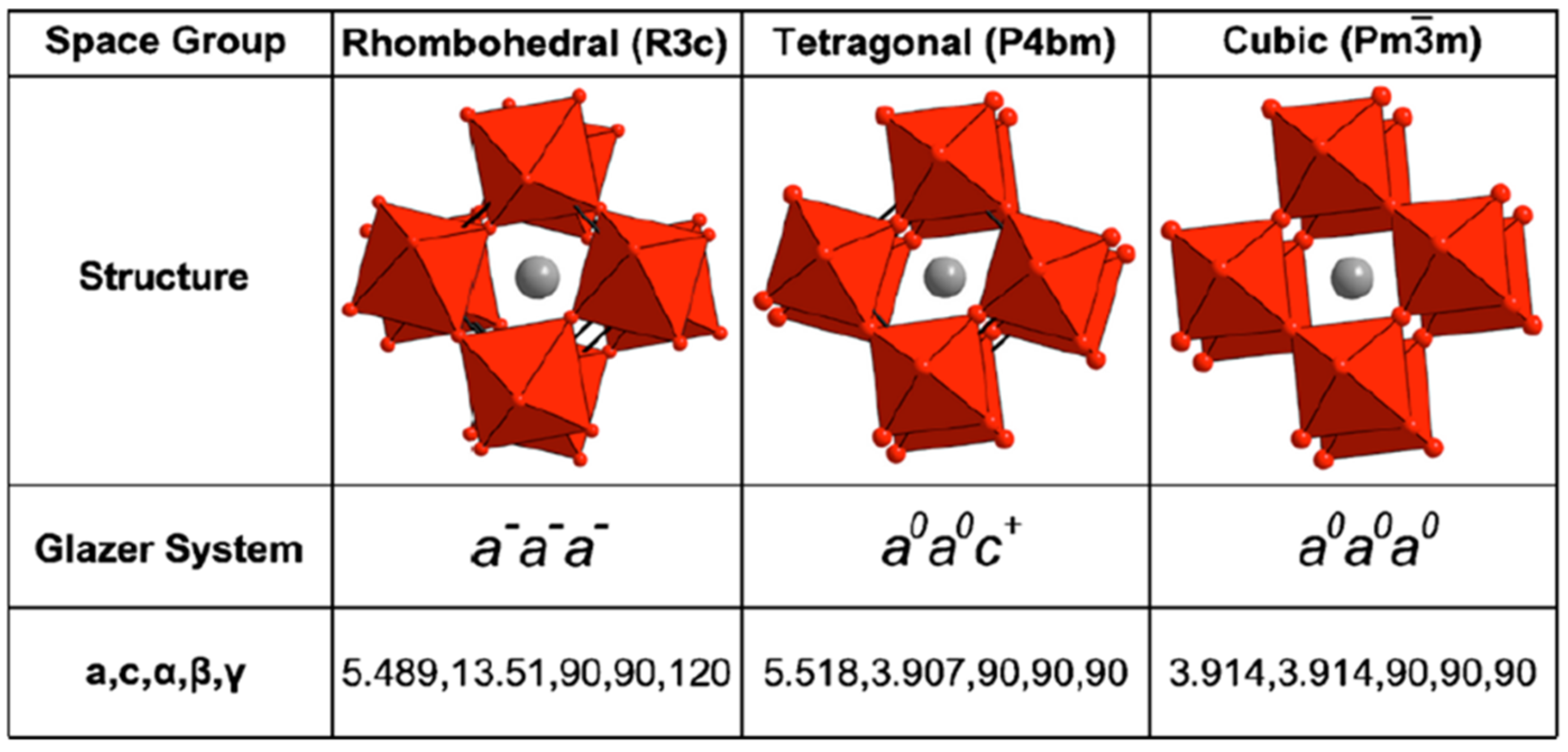
- Glazer, A. The classification of tilted octahedra in perovskites. Acta Crystallogr. Sect. B Struct. Crystallogr. Cryst. Chem. 1972, 28, 3384–3392. [Google Scholar] [CrossRef]
- Stokes, H.T.; Kisi, E.H.; Hatch, D.M.; Howard, C.J. Group-theoretical analysis of octahedral tilting in ferroelectric perovskites. Acta Crystallogr. Sect. B Struct. Sci. 2002, 58, 934–938. [Google Scholar] [CrossRef]
- Simons, H.; Daniels, J.; Jo, W.; Dittmer, R.; Studer, A.; Avdeev, M.; Rodel, J.; Hoffman, M. Electric-field-induced strain mechanisms in lead-free 94%(Bi1/2Na1/2)TiO3–6%BaTiO3. Appl. Phys. Lett. 2011, 98, 082901. [Google Scholar] [CrossRef]
- Kay, H.F.; Vousden, P. XCV. Symmetry changes in barium titanate at low temperatures and their relation to its ferroelectric properties. London Edinburgh Dublin Philos. Mag. J. Sci. 1949, 40, 1019–1040. [Google Scholar] [CrossRef]
- Von Hippel, A. Ferroelectricity, domain structure, and phase transitions of barium titanate. Rev. Mod. Phys. 1950, 22. [Google Scholar] [CrossRef]
- Kay, H.; Wellard, H.; Vousden, P. Atomic positions and optical properties of barium titanate. Nature 1949, 163, 636–637. [Google Scholar] [CrossRef]
- Evans, H. The crystal structure of tetragonal barium titanate. Acta Crystallogr. 1951, 4, 377. [Google Scholar] [CrossRef]
- Evans, H.T. An X-ray diffraction study of tetragonal barium titanate. Acta Crystallogr. 1961, 14, 1019–1026. [Google Scholar] [CrossRef]
- Levin, I.; Reaney, I.M.; Anton, E.M.; Jo, W.; Rödel, J.; Pokorny, J.; Schmitt, L.A.; Kleebe, H.J.; Hinterstein, M.; Jones, J.L. Local structure, pseudosymmetry, and phase transitions in Na1/2Bi1/2TiO3–K1/2Bi1/2TiO3 ceramics. Phys. Rev. B 2013, 87. [Google Scholar] [CrossRef]
- Zhang, N.; Yokota, H.; Glazer, A.M.; Ren, Z.; Keen, D.; Keeble, D.S.; Thomas, P.A.; Ye, Z.-G. The missing boundary in the phase diagram of PbZr1−xTixO3. Nature Commun. 2014, 5. [Google Scholar] [CrossRef] [PubMed]
- Subbarao, E.C.; McQuarrie, M.C.; Buessem, W.R. Domain effects in polycrystalline barium titanate. J. Appl. Phys. 1957, 28, 1194–1200. [Google Scholar] [CrossRef]
- Baerwald, H.G. Thermodynamic theory of ferroelectric ceramics. Phys. Rev. 1957, 105, 480–486. [Google Scholar] [CrossRef]
- Daniels, J.E.; Jo, W.; Rodel, J.; Jones, J.L. Electric-field-induced phase transformation at a lead-free morphotropic phase boundary: Case study in a 93%(Bi0.5Na0.5)TiO3–7%BaTiO3 piezoelectric ceramic. Appl. Phys. Lett. 2009, 95. [Google Scholar] [CrossRef]
- Hinterstein, M.; Knapp, M.; Holzel, M.; Jo, W.; Cervellino, A.; Ehrenberg, H.; Fuess, H. Field-induced phase transition in Bi1/2Na1/2TiO3-based lead-free piezoelectric ceramics. J. Appl. Crystallogr. 2010, 43, 1314–1321. [Google Scholar] [CrossRef]
- Royles, A.; Bell, A.; Jephcoat, A.; Kleppe, A.; Milne, S.; Comyn, T. Electric-field-induced phase switching in the lead free piezoelectric potassium sodium bismuth titanate. Appl. Phys. Lett. 2010, 97. [Google Scholar] [CrossRef]
- Rubio-Marcos, F.; Reinosa, J.J.; Vendrell, X.; Romero, J.J.; Mestres, L.; Leret, P.; Fernández, J.F.; Marchet, P. Structure, microstructure and electrical properties of Cu2+ doped (K,Na,Li)(Nb,Ta,Sb)O3 piezoelectric ceramics. Ceram. Int. 2013, 39, 4139–4149. [Google Scholar] [CrossRef]
- Picht, G.; Töpfer, J.; Hennig, E. Structural properties of (Bi0.5Na0.5)1–xBaxTiO3 lead-free piezoelectric ceramics. J. Eur. Ceram. Soc. 2010, 30, 3445–3453. [Google Scholar] [CrossRef]
- Mendiola, J.; Pardo, L. A XRD study of 90° domains in tetragonal PLZT under poling. Ferroelectrics 1984, 54, 199–202. [Google Scholar] [CrossRef]
- Mendiola, J.; Pardo, L.; Carmona, F.; Gonzalez, A. Study of poling on calcium modified PbTiO3 piezoceramics. Ferroelectrics 1990, 109, 125–130. [Google Scholar] [CrossRef]
- Bai, F.; Wang, N.; Li, J.; Viehland, D.; Gehring, P.M.; Xu, G.; Shirane, G. X-ray and neutron diffraction investigations of the structural phase transformation sequence under electric field in 0.7Pb(Mg1/3Nb2/3)–0.3PbTiO3 crystal. J. Appl. Phys. 2004, 96, 1620–1627. [Google Scholar] [CrossRef]
- Jones, J.L.; Slamovich, E.B.; Bowman, K.J. Domain texture distributions in tetragonal lead zirconate titanate by X-ray and neutron diffraction. J. Appl. Phys. 2005, 97. [Google Scholar] [CrossRef]
- Zhang, X.; Lei, C.; Chen, K. Ferroelectric 90° domain evaluation in tetragonal Pb(Mg1/3Nb2/3)O3–PbTiO3 ceramics. J. Am. Ceram. Soc. 2005, 88, 335–338. [Google Scholar] [CrossRef]
- Endriss, A.; Hammer, M.; Hoffmann, M.J.; Kolleck, A.; Schneider, G.A. Microscopic and macroscopic ferroelectric–ferroelastic and piezoelectric behavior of PZT ceramics. J. Eur. Ceram. Soc. 1999, 19, 1229–1231. [Google Scholar] [CrossRef]
- Hall, D.; Steuwer, A.; Cherdhirunkorn, B.; Mori, T.; Withers, P. A high energy synchrotron X-ray study of crystallographic texture and lattice strain in soft lead zirconate titanate ceramics. J. Appl. Phys. 2004, 96, 4245–4252. [Google Scholar] [CrossRef]
- Rogan, R.C.; Üstündag, E.; Clausen, B.; Daymond, M.R. Texture and strain analysis of the ferroelastic behavior of Pb(Zr,Ti)O3 by in situ neutron diffraction. J. Appl. Phys. 2003, 93, 4104–4111. [Google Scholar] [CrossRef]
- Cullity, B.; Stock, S. Elements of X-ray Diffraction, 3rd ed.; Prentice-Hall: Upper Saddle River, NJ, USA, 2001. [Google Scholar]
- Guinebretière, R. X-Ray Diffraction by Polycrystalline Materials; ISTE Ltd.: London, UK, 2013. [Google Scholar]
- Newnham, R.E. Properties of Materials: Anisotropy, Symmetry, Structure: Anisotropy, Symmetry, Structure; Oxford University Press: Oxford, UK, 2004. [Google Scholar]
- Fuentes-Cobas, L. Synchrotron radiation diffraction and scattering in ferroelectrics. In Multifunctional Polycrystalline Ferroelectric Materials; Pardo, L., Ricote, J., Eds.; Springer: Dordrecht, The Netherlands, 2011; Volume 140, pp. 217–280. [Google Scholar]
- Kalyani, A.K.; Khatua, D.K.; Loukya, B.; Datta, R.; Fitch, A.N.; Senyshyn, A.; Ranjan, R. Metastable monoclinic and orthorhombic phases and electric field induced irreversible phase transformation at room temperature in the lead-free classical ferroelectric BaTiO3. Phys. Rev. B 2015, 91. [Google Scholar] [CrossRef]
- Noheda, B.; Cox, D.; Shirane, G.; Gonzalo, J.; Cross, L.; Park, S. A monoclinic ferroelectric phase in the Pb (Zr1–xTix)O3 solid solution. Appl. Phys. Lett. 1999, 74, 2059–2061. [Google Scholar] [CrossRef]
- Gorfman, S.; Keeble, D.S.; Glazer, A.M.; Long, X.; Xie, Y.; Ye, Z.-G.; Collins, S.; Thomas, P.A. High-resolution X-ray diffraction study of single crystals of lead zirconate titanate. Phys. Rev. B 2011, 84. [Google Scholar] [CrossRef]
- Solanki, R.S.; Mishra, S.K.; Senyshyn, A.; Yoon, S.; Baik, S.; Shin, N.; Pandey, D. Confirmation of the monoclinic Cc space group for the ground state phase of Pb(Zr0.525Ti0.475)O3(PZT525): A combined synchrotron X-ray and neutron powder diffraction study. Appl. Phys. Lett. 2013, 102. [Google Scholar]
- Wojdyr, M. Fityk: A general-purpose peak fitting program. J. Appl. Crystallogr. 2010, 43, 1126–1128. [Google Scholar] [CrossRef]
- Daniels, J.; Jones, J.; Finlayson, T. Characterization of domain structures from diffraction profiles in tetragonal ferroelastic ceramics. J. Phys. D Appl. Phys. 2006, 39. [Google Scholar] [CrossRef]
- Laulhé, C.; Hippert, F.; Bellissent, R.; Simon, A.; Cuello, G.J. Local structure in BaTi1−xZrxO3 relaxors from neutron pair distribution function analysis. Phys. Rev. B 2009, 79. [Google Scholar] [CrossRef]
- Datta, K.; Richter, A.; Göbbels, M.; Neder, R.; Mihailova, B. Atomistic origin of huge response functions at the morphotropic phase boundary of (1−x)Na0.5Bi0.5TiO3−xBaTiO3. Phys. Rev. B 2014, 90. [Google Scholar] [CrossRef]
- Juhás, P.; Davis, T.; Farrow, C.L.; Billinge, S.J. PDFgetX3: a rapid and highly automatable program for processing powder diffraction data into total scattering pair distribution functions. J. Appl. Crystallogr. 2013, 46, 560–566. [Google Scholar] [CrossRef]
- Torres, M.; Pardo, L.; Ricote, J.; Fuentes-Cobas, L.E.; Rodriguez, B.J.; Calzada, M.L. Fabricating ordered functional nanostructures onto polycrystalline substrates from the bottom-up. J. Nanopart. Res. 2012, 14, 1–10. [Google Scholar] [CrossRef]
- Wcislak, L.; Schneider, J.R.; Tschentscher, T.; Klein, H.; Bunge, H.J. Hard X-ray texture measurements with an on-line image plate detector. Nucl. Instrum. Methods Phys. Res. Sect. A 2001, 467–468, 1257–1260. [Google Scholar] [CrossRef]
- He, B.B. Two-Dimensional X-Ray Diffraction; John Wiley & Sons: Hoboken, NJ, USA, 2009. [Google Scholar]
- Drakopoulos, M.; Connolley, T.; Reinhard, C.; Atwood, R.; Magdysyuk, O.; Vo, N.; Hart, M.; Connor, L.; Humphreys, B.; Howell, G.; et al. I12: The joint engineering, environment and processing (JEEP) beamline at diamond light source. J. Synchrotron Radiat. 2015, 22, 828–838. [Google Scholar] [CrossRef] [PubMed]
- Daniels, J.E.; Drakopoulos, M. High-energy X-ray diffraction using the Pixium 4700 flat-panel detector. J. Synchrotron Radiat. 2009, 16, 463–468. [Google Scholar] [CrossRef] [PubMed]
- Veerappan, C.; Richardson, J.; Walker, R.; Li, D.-U.; Fishburn, M.W.; Maruyama, Y.; Stoppa, D.; Borghetti, F.; Gersbach, M.; Henderson, R.K. A 160 × 128 single-photon image sensor with on-pixel 55ps 10b time-to-digital converter. In Proceedings of the Solid-State Circuits Conference Digest of Technical Papers (ISSCC), 2011 IEEE International, San Francisco, CA, USA, 20–24 February 2011; pp. 312–314.
- Henrich, B.; Bergamaschi, A.; Broennimann, C.; Dinapoli, R.; Eikenberry, E.F.; Johnson, I.; Kobas, M.; Kraft, P.; Mozzanica, A.; Schmitt, B. PILATUS: A single photon counting pixel detector for X-ray applications. Nucl. Instrum. Methods Phys. Res. Sect. A 2009, 607, 247–249. [Google Scholar] [CrossRef]
- Johnson, I.; Bergamaschi, A.; Buitenhuis, J.; Dinapoli, R.; Greiffenberg, D.; Henrich, B.; Ikonen, T.; Meier, G.; Menzel, A.; Mozzanica, A.; et al. Capturing dynamics with Eiger, a fast-framing X-ray detector. J. Synchrotron Radiat. 2012, 19, 1001–1005. [Google Scholar] [CrossRef] [PubMed]
- Fuentes-Cobas, L.E.; Muñoz-Romero, A.; Montero-Cabrera, M.E.; Fuentes-Montero, L.; Fuentes-Montero, M.E. Predicting the coupling properties of axially-textured materials. Materials 2013, 6, 4967–4984. [Google Scholar] [CrossRef]
- Wenk, H.-R.; Lutterotti, L.; Vogel, S. Texture analysis with the new HIPPO TOF diffractometer. Nucl. Instrum. Methods Phys. Res. Sect. A 2003, 515, 575–588. [Google Scholar] [CrossRef]
- Cruz-Gandarilla, F.; Salcedo-Garrido, A.; Avalos, M.; Bolmaro, R.; Baudin, T.; Cabañas-Moreno, J.; Dorantes-Rosales, H. EBSD characterization of an IF steel processed by Accumulative Roll Bonding. In Proceedings of the 17th International Conference on Textures of Materials (ICOTOM), Dresden, Germany, 24–29 August 2014.
- Reyes-Ruiz, C.; Figueroa, I.A.; Braham, C.; Cabrera, J.M.; Alfonso, I.; Gonzalez, G. Texture and lattice distortion study of an Al-6061-T6 alloy produced by ECAP. Mater. Trans. 2015, 56, 1781–1786. [Google Scholar] [CrossRef]
- Sáenz-Trevizo, A.; Amézaga-Madrid, P.; Fuentes-Cobas, L.; Pizá-Ruiz, P.; Antúnez-Flores, W.; Ornelas-Gutiérrez, C.; Pérez-García, S.; Miki-Yoshida, M. Microstructural, chemical and textural characterization of ZnO nanorods synthesized by aerosol assisted chemical vapor deposition. Mater. Charact. 2014, 98, 215–221. [Google Scholar] [CrossRef]
- Fuentes-Montero, L.; Montero-Cabrera, M.E.; Fuentes-Cobas, L. The software package ANAELU for X-ray diffraction analysis using two-dimensional patterns. J. Appl. Crystallogr. 2010, 44, 241–246. [Google Scholar] [CrossRef]
- Chen, C.-S.; Chen, P.-Y.; Tu, C.-S. Polar nanoregions and dielectric properties in high-strain lead-free 0.93(Bi1/2Na1/2)TiO3–0.07BaTiO3 piezoelectric single crystals. J. Appl. Phys. 2014, 115. [Google Scholar] [CrossRef]
- Schönau, K.A.; Knapp, M.; Kungl, H.; Hoffmann, M.J.; Fuess, H. In situ synchrotron diffraction investigation of morphotropic Pb[Zr1−xTix]O3 under an applied electric field. Phys. Rev. B 2007, 76. [Google Scholar] [CrossRef]
- Daniels, J.E.; Pramanick, A.; Jones, J.L. Time-Resolved Characterization of Ferroelectrics Using High-Energy X-Ray Diffraction. In Proceedings of the 17th IEEE International Symposium on Applications of Ferroelectrics, Santa Fe, NM, USA, 24–27 February 2009.
- Daniels, J.E.; Jo, W.; Rödel, J.; Honkimäki, V.; Jones, J.L. Electric-field-induced phase-change behavior in (Bi0.5Na0.5)TiO3–BaTiO3–(K0.5Na0.5)NbO3: A combinatorial investigation. Acta Mater. 2010, 58, 2103–2111. [Google Scholar] [CrossRef]
- Pramanick, A.; Damjanovic, D.; Daniels, J.E.; Nino, J.C.; Jones, J.L. Origins of electro-mechanical coupling in polycrystalline ferroelectrics during subcoercive electrical loading. J. Am. Ceram. Soc. 2011, 94, 293–309. [Google Scholar] [CrossRef]
- Hall, D.A.; Azough, F.; Middleton-Stewart, N.; Cernik, R.J.; Freer, R.; Mori, T.; Kungl, H.; Curfs, C. In-Situ X-ray diffraction study of ferroelectric domain switching in orthorhombic NKN ceramics. Funct. Mater. Lett. 2010, 3, 31–34. [Google Scholar] [CrossRef]
- Hinterstein, M.; Rouquette, J.; Haines, J.; Papet, P.; Knapp, M.; Glaum, J.; Fuess, H. Structural description of the macroscopic piezo- and ferroelectric properties of lead zirconate titanate. Phys. Rev. Lett. 2011, 107. [Google Scholar] [CrossRef] [PubMed]
- Wooldridge, J.; Ryding, S.; Brown, S.; Burnett, T.L.; Cain, M.G.; Cernik, R.; Hino, R.; Stewart, M.; Thompson, P. Simultaneous measurement of X-ray diffraction and ferroelectric polarization data as a function of applied electric field and frequency. J. Synchrotron Radiat. 2012, 19, 710–716. [Google Scholar] [CrossRef] [PubMed]
- Fancher, C.M.; Iamsasri, T.; Blendell, J.E.; Bowman, K.J. Effect of crystallographic texture on the field-induced-phase transformation behavior of Bi0.5Na0.5TiO3−7BaTiO3−2K0.5Na0.5NbO3. Mater. Res. Lett. 2013, 1, 156–160. [Google Scholar] [CrossRef]
- Daniel, L.; Hall, D.; Webber, K.; King, A.; Withers, P. Identification of crystalline elastic anisotropy in PZT ceramics from in-situ blocking stress measurements. J. Appl. Phys. 2014, 115. [Google Scholar] [CrossRef]
- Daniel, L.; Hall, D.; Koruza, J.; Webber, K.; King, A.; Withers, P. Revisiting the blocking force test on ferroelectric ceramics using high energy X-ray diffraction. J. Appl. Phys. 2015, 117. [Google Scholar] [CrossRef]
- Moriyoshi, C.; Hiramoto, S.; Ohkubo, H.; Kuroiwa, Y.; Osawa, H.; Sugimoto, K.; Kimura, S.; Takata, M.; Kitanaka, Y.; Noguchi, Y. Synchrotron radiation study on time-resolved tetragonal lattice strain of BaTiO3 under electric field. Jpn. J. Appl. Phys. 2011, 50. [Google Scholar] [CrossRef]
- Ogino, M.; Noguchi, Y.; Kitanaka, Y.; Miyayama, M.; Moriyoshi, C.; Kuroiwa, Y. Polarization rotation and monoclinic distortion in ferroelectric (Bi0.5Na0.5)TiO3–BaTiO3 single crystals under electric fields. Crystals 2014, 4, 273–295. [Google Scholar] [CrossRef]
- Hinterstein, M.; Schmitt, L.A.; Hoelzel, M.; Jo, W.; Rödel, J.; Kleebe, H.-J.; Hoffman, M. Cyclic electric field response of morphotropic Bi1/2Na1/2TiO3-BaTiO3 piezoceramics. Appl. Phys. Lett. 2015, 106. [Google Scholar] [CrossRef]
- Hinterstein, M.; Hoelzel, M.; Rouquette, J.; Haines, J.; Glaum, J.; Kungl, H.; Hoffman, M. Interplay of strain mechanisms in morphotropic piezoceramics. Acta Mater. 2015, 94, 319–327. [Google Scholar] [CrossRef]
- Fuentes-Cobas, L.E.; Pardo, L.; Montero-Cabrera, M.E.; Plaisier, J.R.; García, A.; Brebøl, K.; Mercadelli, E.; Galassi, C. The 0.96(Bi0.5Na0.5)TiO3–0.04BaTiO3 crystal structure: A high-Q, high-counting statistics synchrotron diffraction analysis. Cryst. Res. Technol. 2014, 49, 190–194. [Google Scholar] [CrossRef]
- Simons, H.; Daniels, J.E.; Studer, A.J.; Jones, J.L.; Hoffman, M. Measurement and analysis of field-induced crystallographic texture using curved position-sensitive diffraction detectors. J. Electroceram. 2014, 32, 283–291. [Google Scholar] [CrossRef]
- Rodriguez-Carvajal, J. Recent developments of the prrogram FULLPROF. Comm. Powder Diffr. IUCr. Newsl. 2001, 26, 12–19. [Google Scholar]
- Tutuncu, G.; Motahari, M.; Daymond, M.R.; Ustundag, E. A modified Rietveld method to model highly anisotropic ceramics. Acta Mater. 2012, 60, 1494–1502. [Google Scholar] [CrossRef]
- Matthies, S.; Lutteroti, L.; Wenk, H.R. Advances in texture analysis from diffraction spectra. J. Appl. Crystallogr. 1997, 30, 31–42. [Google Scholar] [CrossRef]
- Lutterotti, L.; Chateigner, D.; Ferrari, S.; Ricote, J. Texture, residual stress and structural analysis of thin films using a combined X-ray analysis. Thin Solid Films 2004, 450, 34–41. [Google Scholar] [CrossRef]
- Fertey, P.; Alle, P.; Wenger, E.; Dinkespiler, B.; Cambon, O.; Haines, J.; Hustache, S.; Medjoubi, K.; Picca, F.; Dawiec, A. Diffraction studies under in situ electric field using a large-area hybrid pixel XPAD detector. J. Appl. Crystallogr. 2013, 46, 1151–1161. [Google Scholar] [CrossRef]
- Oddershede, J.; Majkut, M.; Cao, Q.; Schmidt, S.; Wright, J.P.; Kenesei, P.; Daniels, J. Quantitative grain-scale ferroic domain volume fractions and domain switching strains from three-dimensional X-ray diffraction data. J. Appl. Crystallogr. 2015, 48, 882–889. [Google Scholar] [CrossRef] [Green Version]
- Fuentes-Cobas, L.E.; Montero-Cabrera, M.E.; Garcia, A.; Brebol, K.; Mercadeli, E.; Galassi, C.; Pardo, L. Efecto del campo eléctrico en la estructura cristalina de cerámicas submicroestructuradas de (1–x)(Bi0.5Na0.5)TiO3–xBaTiO3 con composición próxima a la frontera morfotrópica. In Proceedings of the X Reunión Nacional de Electrocerámica, Madrid, Spain, 13–15 June 2011; p. 30.
- Rao, B.N.; Ranjan, R. Electric-field-driven monoclinic-to-rhombohedral transformation in Na1/2Bi1/2TiO3. Phys. Rev. B Condens. Matter Mater. Phys. 2012, 86. [Google Scholar] [CrossRef]
- Gröting, M.; Kornev, I.; Dkhil, B.; Albe, K. Pressure-induced phase transitions and structure of chemically ordered nanoregions in the lead-free relaxor ferroelectric Na1/2Bi1/2TiO3. Phys. Rev. B 2012, 86. [Google Scholar] [CrossRef]
- Garg, R.; Rao, B.N.; Senyshyn, A.; Krishna, P.; Ranjan, R. Lead-free piezoelectric system (Na0.5Bi0.5)TiO3–BaTiO3: Equilibrium structures and irreversible structural transformations driven by electric field and mechanical impact. Phys. Rev. B 2013, 88. [Google Scholar] [CrossRef]
- Aksel, E.; Forrester, J.S.; Kowalski, B.; Deluca, M.; Damjanovic, D.; Jones, J.L. Structure and properties of Fe-modified Na0.5Bi0.5TiO3 at ambient and elevated temperature. Phys. Rev. B 2012, 85. [Google Scholar] [CrossRef]
- Usher, T.M.; Forrester, J.S.; dela Cruz, C.R.; Jones, J.L. Crystal structure of 0.96(Na0.5Bi0.5TiO3)–0.04(BaTiO3) from combined refinement of x-ray and neutron diffraction patterns. Appl. Phys. Lett. 2012, 101. [Google Scholar] [CrossRef]
- Cheng, S.-Y.; Shieh, J.; Lu, H.-Y.; Shen, C.-Y.; Tang, Y.-C.; Ho, N.-J. Structure analysis of bismuth sodium titanate-based A-site relaxor ferroelectrics by electron diffraction. J. Eur. Ceram. Soc. 2013, 33, 2141–2153. [Google Scholar] [CrossRef]
- Carter, J.; Aksel, E.; Iamsasri, T.; Forrester, J.S.; Chen, J.; Jones, J.L. Structure and ferroelectricity of nonstoichiometric (Na0.5Bi0.5)TiO3. Appl. Phys. Lett. 2014, 104. [Google Scholar] [CrossRef]
- Iamsasri, T.; Tutuncu, G.; Uthaisar, C.; Wongsaenmai, S.; Pojprapai, S.; Jones, J.L. Electric field-induced phase transitions in Li-modified Na0.5K0.5NbO3 at the polymorphic phase boundary. J. Appl. Phys. 2015, 117. [Google Scholar] [CrossRef]
- Montero-Cabrera, M.E.; Pardo, L.; García, A.; Fuentes-Montero, M.E.; Ballinas-Casarrubias, M.L.; Fuentes-Cobas, L.E. The global and local symmetries of nanostructured ferroelectric relaxor 0.94(Bi0.5Na0.5)TiO3–0.06BaTiO3. Ferroelectrics 2014, 469, 50–60. [Google Scholar] [CrossRef]
- Rao, B.N.; Datta, R.; Chandrashekaran, S.S.; Mishra, D.K.; Sathe, V.; Senyshyn, A.; Ranjan, R. Local structural disorder and its influence on the average global structure and polar properties in Na0.5Bi0.5TiO3. Phys. Rev. B 2013, 88. [Google Scholar] [CrossRef]
- Ehmke, M.C.; Khansur, N.H.; Daniels, J.E.; Blendell, J.E.; Bowman, K.J. Resolving structural contributions to the electric-field-induced strain in lead-free (1−x)Ba(Zr0.2Ti0.8)O3−x(Ba0.7Ca0.3)TiO3 piezoceramics. Acta Mater. 2014, 66, 340–348. [Google Scholar] [CrossRef]
- Rehr, J.J.; Albers, R.C. Theoretical approaches to X-ray absorption fine structure. Rev. Mod. Phys. 2000, 72, 621–654. [Google Scholar] [CrossRef]
- Teo, B.K. EXAFS: Basics Principles and Data Analysis, 1st ed.; Springer-Verlag: Berlin Heidelberg, Germany, New York, Tokyo; Bell Telephone Laboratories, Incorprorated: Murray Hill, NJ, USA, 1986. [Google Scholar]
- Koningsberger, D.C.; Prins, R.E. X-Ray Absorption: Principles, Applications, Techniques of EXAFS, SEXAFS, and XANES; John Wiley and Sons: New York, NY, USA, 1988; Volume 92, p. 684. [Google Scholar]
- Calvin, S. XAFS for Everyone; CRC Press: Boca Raton, FL, USA, 2013; p. 457. [Google Scholar]
- Lee, J.H.; Choi, H.J.; Lee, D.; Kim, M.G.; Bark, C.W.; Ryu, S.; Oak, M.A.; Jang, H.M. Variations of ferroelectric off-centering distortion and 3d-4p orbital mixing in La-doped BiFeO3 multiferroics. Phys. Rev. B 2010, 82. [Google Scholar] [CrossRef]
- García-Guaderrama, M.; Montero-Cabrera, M.E.; Morán, E.; Alario-Franco, M.A.; Fuentes-Cobas, L.E.; Macías-Ríos, E.; Esparza-Ponce, H.E.; Fuentes-Montero, M.E. Long-and short-range structure of ferrimagnetic iron—Chromium maghemites. Inorg. Chem. 2015, 54, 11200–11208. [Google Scholar] [CrossRef] [PubMed]
- Wong, J.; Lytle, F.W.; Messmer, R.P.; Maylotte, D.H. K-edge absorption spectra of selected vanadium compounds. Phys. Rev. B 1984, 30, 5596–5610. [Google Scholar] [CrossRef]
- Eustace, D.A.; McComb, D.W.; Craven, A.J. Probing magnetic order in EELS of chromite spinels using both multiple scattering (FEFF8.2) and DFT (WIEN2k). Micron 2010, 41, 547–553. [Google Scholar] [CrossRef] [PubMed]
- Farges, F. Ab initio and experimental pre-edge investigations of the Mn K-edge XANES in oxide-type materials. Phys. Rev. B 2005, 71. [Google Scholar] [CrossRef]
- Vedrinskii, R.V.; Kraizman, V.L.; Novakovich, A.A.; Demekhin, P.V.; Urazhdin, S.V. Pre-edge fine structure of the 3d atom K X-ray absorption spectra and quantitative atomic structure determinations for ferroelectric perovskite structure crystals. J. Phys. Condes. Matter 1998, 10, 9561–9580. [Google Scholar] [CrossRef]
- Montero-Cabrera, M.E.; Sáez-Puche, R.; Climent-Pascual, E.; Morán, E.; Fuentes, M.E.; Fuentes-Cobas, L.E. XAFS characterization of zircon and scheelite RCrO4 (R = Er and Y) polymorphs. In Proceedings of the 14th International Conference on X-Ray Absorption Fine Structure (XAFS XIV), Camerino, Italy, 26–31 July 2009; p. PS1 110.
- Shanthakumar, P.; Balasubramanian, M.; Pease, D.M.; Frenkel, A.I.; Potrepka, D.M.; Kraizman, V.; Budnick, J.I.; Hines, W.A. X-ray study of the ferroelectric [Ba0.6Sr0.4][(YTa)0.03Ti0.94]O3. Phys. Rev. B 2006, 74. [Google Scholar] [CrossRef]
- Frenkel, A.I.; Pease, D.M.; Giniewicz, J.; Stern, E.A.; Brewe, D.L.; Daniel, M.; Budnick, J. Concentration-dependent short-range order in the relaxor ferroelectric (1–x)Pb(Sc,Ta)O3–xPbTiO3. Phys. Rev. B 2004, 70. [Google Scholar] [CrossRef]
- Yamamoto, T. Assignment of pre-edge peaks in K-edge X-ray absorption spectra of 3d transition metal compounds: electric dipole or quadrupole? X-Ray Spectrom. 2008, 37, 572–584. [Google Scholar] [CrossRef]
- Mesquita, A.; Michalowicz, A.; Mastelaro, V.R. Local order and electronic structure of Pb1–xLaxZr0.40Ti0.60O3 materials and its relation with ferroelectric properties. J. Appl. Phys. 2012, 111, 104110–104116. [Google Scholar] [CrossRef]
- Mesquita, A.; Michalowicz, A.; Mastelaro, V. XANES measurements probing the local order and electronic structure of Pb1−xBaxZr0.40Ti0.60O3 ferroelectric materials. J. Alloys Compd. 2015, 640, 355–361. [Google Scholar] [CrossRef]
- Kempet, W.; Marungsri, B.; Yimniran, R.; Klysubun, W.; Pojprapai, S. Investigation of the unit cell distortion in PZT ceramic via in-situ XAS technique. Ferroelectrics 2013, 453, 106–112. [Google Scholar] [CrossRef]
- Levin, I.; Cockayne, E.; Krayzman, V.; Woicik, J.C.; Lee, S.; Randall, C.A. Local structure of Ba(Ti,Zr)O3 perovskite-like solid solutions and its relation to the band-gap behavior. Phys. Rev. B 2011, 83. [Google Scholar] [CrossRef]
- Blanchard, P.E.; Liu, S.; Kennedy, B.J.; Ling, C.D.; Zhang, Z.; Avdeev, M.; Jang, L.-Y.; Lee, J.-F.; Pao, C.-W.; Chen, J.-L. Studying the effects of Zr-doping in (Bi0.5Na0.5)TiO3 via diffraction and spectroscopy. Dalton Trans. 2014, 43. [Google Scholar] [CrossRef]
- Liu, S.; Blanchard, P.E.R.; Zhang, Z.; Kennedy, B.J.; Ling, C.D. Long- and short-range structure studies of KBT-KBZ solid-solutions using synchrotron radiation. Dalton Trans. 2015, 44, 10681–10688. [Google Scholar] [CrossRef] [PubMed]
- Ma, C.; Guo, H.; Beckman, S.P.; Tan, X. Creation and destruction of morphotropic phase boundaries through electrical poling: A case study of lead-free (Bi1/2Na1/2)TiO3–BaTiO3 Piezoelectrics. Phys. Rev. Lett. 2012, 109. [Google Scholar] [CrossRef] [PubMed]
- Kitanaka, Y.; Ogino, M.; Hirano, K.; Noguchi, Y.; Miyayama, M.; Kagawa, Y.; Moriyoshi, C.; Kuroiwa, Y.; Torii, S.; Kamiyama, T. Crystal structural analyses of ferrielectric tetragonal (Bi1/2Na1/2)TiO3–7%BaTiO3 powders and single crystals. Jpn. J. Appl. Phys. 2013, 52. [Google Scholar] [CrossRef]
- Ranjan, R.; Dviwedi, A. Structure and dielectric properties of (Na0.50Bi0.50)1–xBaxTiO3: 0 ≤ x ≤ 0.10. Solid State Commun. 2005, 135, 394–399. [Google Scholar] [CrossRef]
- Dorcet, V.; Trolliard, G. A transmission electron microscopy study of the A-site disordered perovskite Na0.5Bi0.5TiO3. Acta Mater. 2008, 56, 1753–1761. [Google Scholar] [CrossRef]
- Ma, C.; Tan, X. Phase diagram of unpoled lead-free (1–x) (Bi1/2Na1/2)TiO3–xBaTiO3 ceramics. Solid State Commun. 2010, 150, 1497–1500. [Google Scholar] [CrossRef]
- Schmitt, L.A.; Kleebe, H.-J. Single grains hosting two space groups—A transmisision electron microscopy study of a lead-free ferroelectric. Funct. Mater. Lett. 2010, 3, 55–58. [Google Scholar] [CrossRef]
- Pardo, L.; Mercadelli, E.; Garcia, A.; Brebol, K.; Galassi, C. Field-induced phase transition and relaxor character in submicrometer-structured lead-free (Bi0.5Na0.5)0.94Ba0.06TiO3 piezoceramics at the morphotropic phase boundary. IEEE Trans. Ultrason. Ferroelectr. Freq. Control 2011, 58, 1893–1904. [Google Scholar] [CrossRef] [PubMed]
- Pardo, L.; García, A.; Brebol, K.; Mercadelli, E.; Galassi, C. Piezoelectric properties of lead-free submicron-structured (Bi0.5Na0.5)0.94Ba0.06TiO3 ceramics from nanopowders. Smart Mater. Struct. 2010, 19. [Google Scholar] [CrossRef]
- Kholkin, A.L.; Kiselev, D.A.; Bdikin, I.K.; Sternberg, A.; Dkhil, B.; Jesse, S.; Ovchinnikov, O.; Kalinin, S.V. Mapping disorder in polycrystalline relaxors: A piezoresponse force microscopy approach. Materials 2010, 3, 4860–4870. [Google Scholar] [CrossRef]
- Jeong, I.-K.; Darling, T.; Lee, J.-K.; Proffen, T.; Heffner, R.; Park, J.; Hong, K.; Dmowski, W.; Egami, T. Direct observation of the formation of polar nanoregions in Pb (Mg1/3Nb2/3)O3 using neutron pair distribution function analysis. Phys. Rev. Lett. 2005, 94. [Google Scholar] [CrossRef] [PubMed]
- Dittmer, R.; Jo, W.; Webber, K.G.; Jones, J.L.; Rödel, J. Local structure change evidenced by temperature-dependent elastic measurements: Case study on Bi1/2Na1/2TiO3-based lead-free relaxor piezoceramics. J. Appl. Phys. 2014, 115. [Google Scholar] [CrossRef]
- Jo, W.; Rodel, J.; Lee, J.-S.; Baik, Y.-H.; Park, C. Effect of substitution of K for Na on the ferroelectric stability and properties of (Bi1/2Na1/2)TiO3-BaTiO3-(K0.5Na0.5)NbO3. Funct. Mater. Lett. 2010, 3, 41–44. [Google Scholar] [CrossRef]
- Zhang, Q.; Zhao, X.; Sun, R.; Luo, H. Crystal growth and electric properties of lead-free NBT-BT at compositions near the morphotropic phase boundary. Phys. Status Solidi A 2011, 208, 1012–1020. [Google Scholar] [CrossRef]
- Pardo, L.; García, A.; Brebøl, K.; Mercadelli, E.; Galassi, C. Characterization of Nanostructured Phases and Peculiar Phase Transitions in BNBT Lead-Free Piezoceramics. Adv. Sci. Tech. 2014, 90, 12–18. [Google Scholar] [CrossRef]
- Rebuffi, L.; Plaisier, J.R.; Abdellatief, M.; Lausi, A.; Scardi, P. MCX: A synchrotron radiation beamline for X-ray diffraction line profile analysis. Z. Anorg. Allg. Chem. 2014, 640, 3100–3106. [Google Scholar] [CrossRef]
- Rodríguez-Carvajal, J. Recent advances in magnetic structure determination by neutron powder diffraction. Phys. B 1993, 192, 55–69. [Google Scholar] [CrossRef]
- Craciun, F.; Galassi, C.; Birjega, R. Electric-field-induced and spontaneous relaxor-ferroelectric phase transitions in (Na1/2Bi1/2)(1–x)BaxTiO3. J. Appl. Phys. 2012, 112. [Google Scholar] [CrossRef]
- Groszewicz, P.B.; Breitzke, H.; Dittmer, R.; Sapper, E.; Jo, W.; Buntkowsky, G.; Rödel, J. Nanoscale phase quantification in lead-free (Bi1/2Na1/2)TiO3–BaTiO3 relaxor ferroelectrics by means of NMR. Phys. Rev. B 2014, 90. [Google Scholar] [CrossRef]
- Gonzalez, A.M.; Pardo, L.; Montero-Cabrera, M.E.; Fuentes-Cobas, L.E. Analysis of the rhombohedral and tetragonal symmetries coexistence in lead-free 0.94(Bi0.5Na0.5)TiO3–0.06BaTiO3 ceramics from nanopowders. In Proceedings of Piezo 2015, Maribor, Slovenija, 25–28 January 2015. Adv. Appl. Ceram. accepted.
- De Frutos, J.; Jimenez, B. Evolution of the spatial distribution of polarization in lead-calcium ferroelectric ceramics. Ferroelectrics 1992, 126, 341–345. [Google Scholar] [CrossRef]
- Mi, S.-B.; Jin, X.-W.; Cheng, S.; Liu, M.; Lu, L.; Jia, C.-L. Atomic structures of planar defects in 0.95(Na0.5Bi0.5)TiO3–0.05BaTiO3 lead-free piezoelectric thin films. J. Alloys Compd. 2015, 636, 183–186. [Google Scholar] [CrossRef]
- Anthoniappen, J.; Tu, C.S.; Chen, P.Y.; Chen, C.S.; Chiu, S.J.; Lee, H.Y.; Ting, Y.; Wang, S.F.; Chai, C.K. Structural phase stability and electric field induced relaxor–ferroelectric phase transition in (1−x)(Bi0.5Na0.5)TiO3–xBaTiO3 ceramics. J. Alloys Compd. 2015, 618, 120–126. [Google Scholar] [CrossRef]
- Xu, G.; Hiraka, H.; Ohwada, K.; Shirane, G. Dual structures in PZN-xPT ferroelectric relaxors. Appl. Phys. Lett. 2004. [Google Scholar] [CrossRef]
- Chang, W.S.; Lim, L.C.; Yang, P.; Miao, H.; Tu, C.-S.; Chen, Q.; Soh, A.K. Tetragonal micro/nanotwins in 0.91Pb(Zn1/3Nb2/3)O3−0.09PbTiO3 revealed by reciprocal space mapping. Appl. Phys. Lett. 2009, 94. [Google Scholar] [CrossRef]
- Nelmes, R.J.; Piltz, R.O.; Kuhs, W.F.; Tun, Z.; Restori, R. Order-disorder behaviour in the transition of PbTiO3. Ferroelectrics 1990, 108, 165–170. [Google Scholar] [CrossRef]
© 2015 by the authors; licensee MDPI, Basel, Switzerland. This article is an open access article distributed under the terms and conditions of the Creative Commons by Attribution (CC-BY) license (http://creativecommons.org/licenses/by/4.0/).
Share and Cite
Fuentes-Cobas, L.E.; Montero-Cabrera, M.E.; Pardo, L.; Fuentes-Montero, L. Ferroelectrics under the Synchrotron Light: A Review. Materials 2016, 9, 14. https://doi.org/10.3390/ma9010014
Fuentes-Cobas LE, Montero-Cabrera ME, Pardo L, Fuentes-Montero L. Ferroelectrics under the Synchrotron Light: A Review. Materials. 2016; 9(1):14. https://doi.org/10.3390/ma9010014
Chicago/Turabian StyleFuentes-Cobas, Luis E., María E. Montero-Cabrera, Lorena Pardo, and Luis Fuentes-Montero. 2016. "Ferroelectrics under the Synchrotron Light: A Review" Materials 9, no. 1: 14. https://doi.org/10.3390/ma9010014