Article

Effect of Growth Pressure on Epitaxial Graphene Grown on 4H-SiC Substrates by Using Ethene Chemical Vapor Deposition

1
National Research Center of Engineering Technology for Utilization of Functional Ingredients from Botanicals, Hunan Agriculture University, Changsha 410128, China
2
Key Laboratory of Semiconductor Materials Science, Institute of Semiconductors, Chinese Academy of Sciences, P.O. Box 912, Beijing 100083, China
*
Author to whom correspondence should be addressed.
Materials 2015, 8(9), 5586-5596; https://doi.org/10.3390/ma8095263
Submission received: 28 July 2015 / Revised: 18 August 2015 / Accepted: 19 August 2015 / Published: 26 August 2015
(This article belongs to the Section Advanced Materials Characterization)

Abstract

:
The Si(0001) face and C(000-1) face dependences on growth pressure of epitaxial graphene (EG) grown on 4H-SiC substrates by ethene chemical vapor deposition (CVD) was studied using atomic force microscopy (AFM) and micro-Raman spectroscopy (μ-Raman). AFM revealed that EGs on Si-faced substrates had clear stepped morphologies due to surface step bunching. However, This EG formation did not occur on C-faced substrates. It was shown by μ-Raman that the properties of EG on both polar faces were different. EGs on Si-faced substrates were relatively thinner and more uniform than on C-faced substrates at low growth pressure. On the other hand, D band related defects always appeared in EGs on Si-faced substrates, but they did not appear in EG on C-faced substrate at an appropriate growth pressure. This was due to the μ-Raman covering the step edges when measurements were performed on Si-faced substrates. The results of this study are useful for optimized growth of EG on polar surfaces of SiC substrates.

Graphical Abstract

1. Introduction

Epitaxial growth of graphene (EG) is more facile in area and layer thickness control [1] than the classic exfoliation of highly oriented pyrolytic graphite crystals (HOPG) [2]. Growth of wafer-scale and hundreds of square meters of mono-layer EG and few-layer EG has been demonstrated [3,4,5], which paves the way for modern semiconductor applications of graphene [6,7]. Shortly after HOPG was demonstrated by Novoselov K.S. and Geim A.K. [2], Berger C. [8] conducted EG on semi-insulting silicon carbide (SI SiC) by using sublimation of silicon atoms from SI SiC surface at high temperature (S-EG). This method has been proved to be efficient for wafer-scale EG-based microelectronics [9,10]. However, S-EG based on SiC wafer is high energy-consumption and expensive since the thermal decomposition is performed at a temperature higher than 1600 °C using the expensive commercial available SiC wafer as the starting material. An alternative solution is growth of graphene on metal foils, which sharply reduces the process cost because the growth process is performed at a temperature about 1000 °C using metal foil as the starting material. The metal foil, especially industrial Cu foil, is cheap even for hundreds of square meters, which is suitable for large-scale EG fabrication [11,12]. On the other hand, polycrystalline metal foils are conductors, which leads to a necessary transfer process of EG from metal foil to target substrate such as SiO2/Si [13]. The transfer process is a key issue for EG and has been intensively studied. EG transferred from metal foils are polycrystalline, with grain boundaries being random distribution, which hampers the electrical transport properties [14]. In contrast, SiC wafers are semiconductors or semi-insulting, which means that it is not necessary for EG on SiC to be transferred to other target substrates. In addition, SiC substrates are monocrystalline; nano-sized steps appear in the surface of SiC after high temperature annealing [15]. The steps are like ladders, which guide graphene grown on SiC surface smoothly and flatly [16]. Therefore, the electrical transport properties of EG on SiC are superior to those of EG from metal foil [17].
Recently, EG growth on SiC by using chemical vapor deposition (CVD) has been developed [18]. In this growth process, graphene is synthesized by thermal decomposition of carbon precursor instead of sublimation of surface Si atoms from SiC substrate. By both using carbon precursor and controlling the dynamic flow in the chamber [11], various reaction parameters in affecting the number of layers and the defect degree of the synthesized graphene have been reported, such as annealing time, heating ramp rates [19], hydrogen partial pressure [20], and growth time [21]. Among them, EG by CVD process is more versatile than EG by sublimation of Si atoms from SiC surface. For example, CVD process enables the growth rate on SiC substrate lower enough to growth of 1 ML EG [18], which is extremely difficult to achieve in the case of S-EG. Additionally, the CVD process enables doped EG grown on the SiC substrate, which creates more opportunities for the study of graphene applications.
Generally, the surfaces of commercial available nominally on-axis 4H-SiC substrates are Si-terminated or C-terminated. This means that 4H-SiC has two polar faces, i.e., C-face and Si-face. It has been reported that graphene can be grown on Si- and C-faced substrates, respectively [22]. In this paper, we report the CVD growth of EG on both Si- and C-faced 4H-SiC substrates using ethene gas as the carbon precursor. Our proposed approach enables simultaneous growth of EG on Si- and C-faced SiC by both adjusting the flow rate of the carbon precursor and the chamber pressure. In this way, we are able to investigate the growth nature of CVD EG on both polar faces of 4H-SiC.

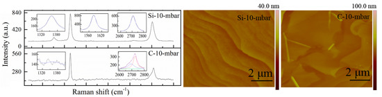
2. Results and Discussion
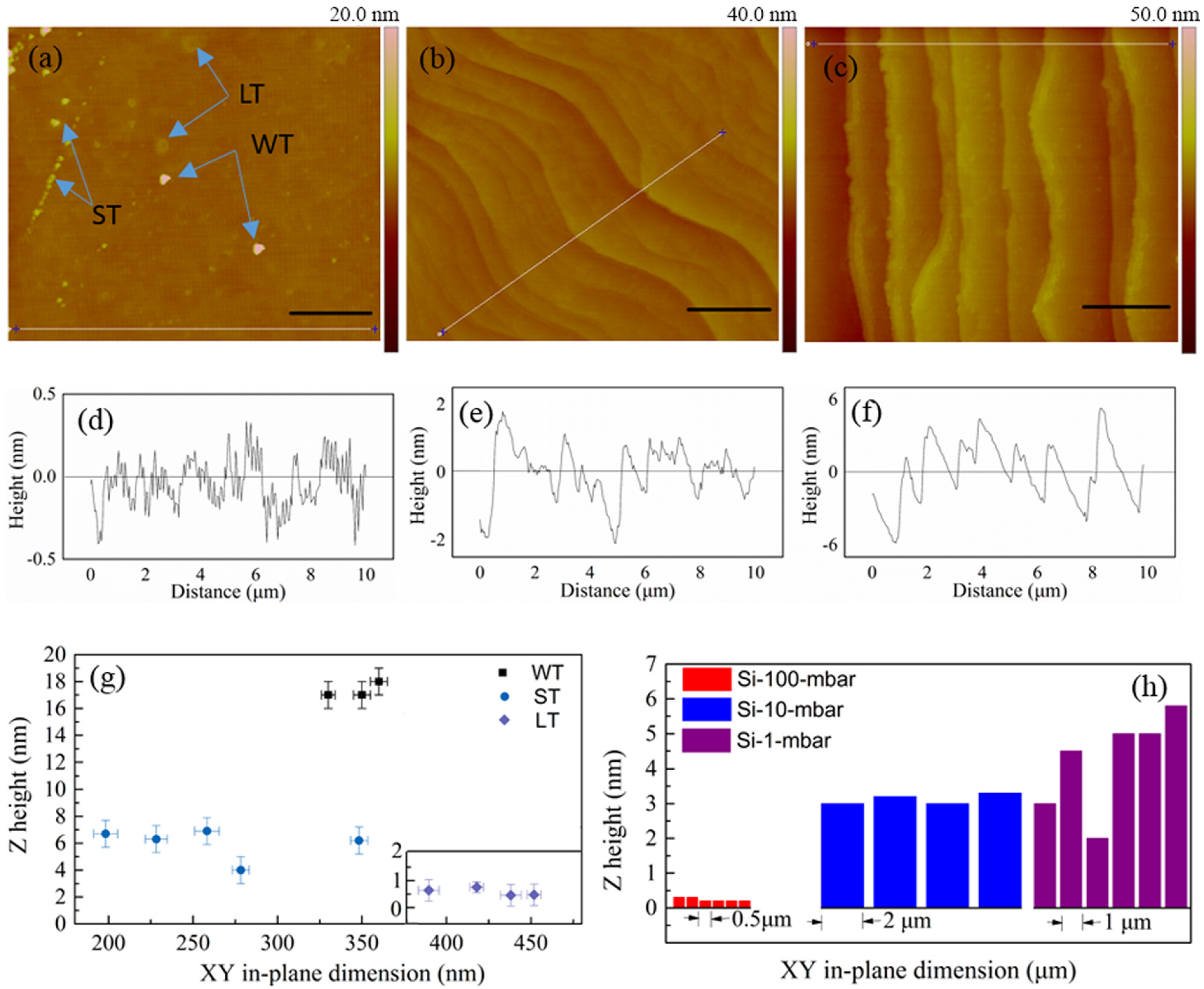
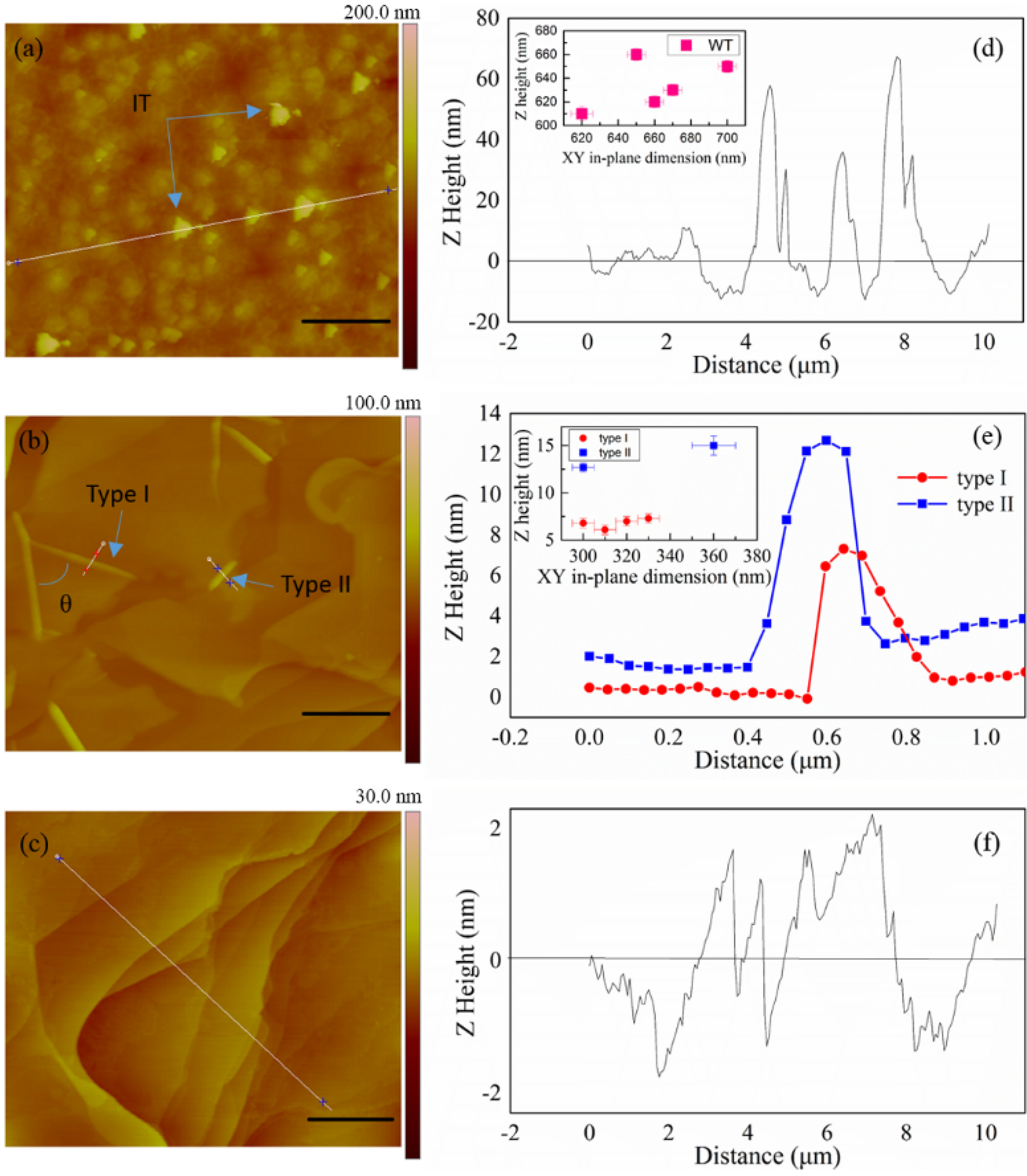
Figure 1 shows the AFM morphologies of EG on Si-face 4H-SiC substrates. The growth pressure plays an important role on the EG morphologies. When the pressure is set to be 100 mbar, which is the highest pressure in our experiments, on the whole the EG surface is smooth, without obvious features except for some individual terraces (Figure 1a). However, small steps of ~0.4 nm height still can be observed (Figure 1d). Terraces in Figure 1a can be categorized into three types: white triangle ones (WT), small triangle ones (ST) and light ones (LT). The arrows in Figure 1a point to these terraces. The sizes of these terraces are distinct. WT is the thickest one while LT is the thinnest one; ST is the smallest one, but LT is the largest one (Figure 1g). The thickness of LT is 0.6~0.8 nm, which is about the thickness of 2 ML graphene [23].
Figure 1. Epitaxial graphene (EG) samples grown on Si-faced 4H-SiC substrates. (a) Sample Si-100-mbar; (b) Sample Si-10-mbar; (c) Sample Si-1-mbar; (df) Atomic force microscopy (AFM) line profiles for the white lines in (a), (b) and (c), respectively; (g) Distribution of three dimensional sizes of individual terraces in (a); (h) Histograms of steps and terraces sizes of EG surfaces on Si-faced substrates. Scale bars: 2 μm.
Materials 08 05263 g001
When the growth pressure decreases, the surface morphologies of the EG are mainly dominated by large steps (Figure 1b,c). These steps are regular, and the mesas between them are covered with small steps. The height of large step increases with growth pressure decrease (Figure 1h), but the height of the small step remains almost in the same range, with a typical value of ~0.5 nm (Figure 1e,f). The widths of the mesas between the steps also vary according to growth pressure. The mesa width of sample Si-10-mbar is ~2 μm, which is about twice of that of Si-1-mbar and four times of that of Si-100-mbar (Figure 1h). The presence of large steps is mainly due to growth at relatively low pressure and high flow rate [18].
Figure 2. EG samples grown on C-faced 4H-SiC substrates. (a) Sample C-100-mbar; (b) Sample C-10-mbar; (c) Sample C-1-mbar; (d) Atomic force microscopy (AFM) line profile for the white line in (a). Inset: distribution of three dimensional sizes of individual terraces in (a); (e) AFM line profiles for two types of ridges in (b). Inset: distribution of three dimensional sizes of ridges in (b); (f) AFM line profile for the white line in (c). Scale bars: 2 μm.
Materials 08 05263 g002
The growth results are distinct at C-faced 4H-SiC substrates. When the growth pressure is set to be 100 mbar, the surface becomes rough (Figure 2a), with an uneven distribution of irregular terraces (IT). The in-plane sizes of the ITs are almost double of that of the WTs (Figure 1g and Figure 2d), and the height of IT is 50~70 nm, which is obviously larger than that of WT. These results show that the efficiency of carbon deposition on C-faced substrate is higher than on the Si-faced substrate at the same growth conditions.
When the growth pressure decreases to 10 mbar, the surface morphologies of the substrate are mainly overlapped by large EG layers. The EG overlayers form flat facets that continuously coat the SiC substrate. There are ridges in some EG. The ridges can be categorized into type-I and type-II ridges. The arrows in Figure 2b point to these ridges. The type-I ridges originate from ridge nodes, as reported by other literatures [24]. A type-I ridge and a type-II ridge is distinction as follows: (i) the maximum height of a type-I ridge is typically less than the height of a type-II ridge (Figure 2e); (ii) a type-II ridge often appears alone, like a short straight line, while type-I ridges often appear as triplets, with a certain intersection angle, and form a crease-like distortion on the surface of a flat graphene facet. The type-I ridges are interconnected, often diverging from a well-defined ridge node by forming a subtended angle θ. In Figure 2b, θ shows preference values of 60° and 120°. These angles are close to high-symmetry directions in the graphene lattice, therefore, it can be deduced that ridge tends to occur along high-symmetry directions in the EG films [24]. When the growth pressure further decreases to 1 mbar, the surface morphologies of the EG are mainly dominated by steps, but the steps are unobvious and irregular (Figure 2c), with a height of 2.5~3 nm (Figure 2f), which indicating EG on C-faced substrate is more complicated than on Si-faced substrate.
To characterize the EG on both the Si- and the C-faced substrates, we perform Raman measurements. Micro-Raman spectroscopy is a non-invasive but powerful technique for graphene characterization [25]. Raman bands at ~1580 cm−1 (G band) and ~2700 cm−1 (2D band) are characteristic peaks for defect-free graphene; band at ~1350 cm−1 (D band) is characteristic for graphene defects such as grain boundaries and edges. The G band originates from in-plane vibration of 𝑠𝑝2 carbon atoms [26] and the 2D band originates from the double-resonance processes of the two phonons with opposite momentum in the highest optical branch near the 𝐾 points in the Brillouin zone [27]. Because the second-order Raman bands of 4H-SiC sit in the range of 1400~1800 cm−1 [28], the D and the G band of graphene on 4H-SiC are complicated. It is necessary to subtract a pristine 4H-SiC Raman spectrum from spectra of EG on 4H-SiC substrates to reveal the graphene spectra [29].
Figure 3 shows typical Raman spectra of six EG samples. The Lorentz fitted D, G and 2D peaks are also shown in Figure 3 as insets. The frequency integrated intensity ratio of the D to G peak (denoted as AD/AG) and the corresponding intensity ratio (ID/IG) are used as characteristic parameters for graphene characterization. There is difference between AD/AG and ID/IG in certain situation [30]. The former is suitable for characterization of graphene with small disorder or perturbations. This is due to the fact that the integrated intensity of each peak represents the probability of the whole Raman process, which considering uncertainty [31]. The latter represents the phonon modes/molecular vibrations involved in the Raman process [32] and is suitable for characterization of graphene with large disorder. However, it is better for ID/IG to combine with full width at half-maximum (FWHM) of Raman peaks when analysis performed since FWHM is a measure of structural disorder [33].
D peaks of sample C-100-mbar, Si-10-mbar and Si-1-mbar are symmetrical and can be fitted by one Lorentz peak, respectively. However, D peaks of sample C-1-mbar and Si-100-mbar are asymmetrical; they can be fitted by three Lorentz peaks, respectively. The D peak of sample C-10-mbar does not appear, which indicating the high quality of EG on C-faced substrate at growth pressure of 10 mbar. The G peaks of all samples can be well fitted by one Lorentz peak, so it is easy to calculate the AD/AG and the ID/IG for sample C-100-mbar, Si-10-mbar and Si-1-mbar, respectively. However, it is out of the question to calculate these values for sample C-1-mbar and Si-100-mbar since they are fitted by multiple Lorentz peaks. The fitting values and the calculated results are listed in Table 1. The values of AD/AG are larger than that of ID/IG, by a factor of 1.3~1.4. However, the change direction of both AD/AG and ID/IG is the same: increasing with increased growth pressure. Judging by the ID/IG ratios of Si-1-mbar, Si-10-mbar and C-100-mbar, high growth pressure can result in the decrease of EG quality. However, this cannot be explicitly applied to C-1-mbar, C-10-mbar and Si-100-mbar, for no ID/IG ratios of these samples are available.
Figure 3. μ-Raman spectra of EG on Si- and C-faced 4H-SiC substrates. The D, G, and 2D band peaks are marked. Insets: Lorentz fits to characterize the width and position of Raman peaks.
Materials 08 05263 g003
G peaks of all samples are almost located at the same position, 1582 ± 1 cm−1, except that of C-1-mbar, 1602 ± 1 cm−1 (Table 1). D peaks of Si-1-mbar and Si-10-mbar are located at 1358 cm−1. D peak of Si-100-mbar is a multi-peak, which can be fitted by three Lorentz peaks, and the center Lorentz peak is located at 1359 cm−1, almost as the same value as that of Si-10-mbar. This means that no Raman shift is seen for graphene grown on Si-faced substrates. Graphene grown on C-faced substrates is more complicated. Although G peaks of C-1-mbar, C-10-mbar and C-100-mbar are not at the same position, they do not take a steady change in direction which is related to the growth pressure.
Table 1. Results of Lorentz fits and grain sizes calculation for EG on polar faces of 4H-SiC substrates.
SamplesD (cm−1)G (cm−1)RatioLa (nm)
XFWHMXFWHMID/IGAD/AG(ID/IG)(AD/AG)
Si-1-mbar1358501582290.100.18167.593.1
C-1-mbar//160230----------------
132835//----------------
136435//----------------
139629//----------------
Si-10-mbar1358451583300.120.19139.688.2
C-10-mbar//158121----------------
Si-100-mbar//158228----------------
134120//----------------
135925//----------------
138730//----------------
C-100-mbar1354441583290.220.3376.150.8
Notes: /: unavailable; ----: no result; X: peak position; (ID/IG): La is calculated by taking ID/IG value.
The average grain sizes La can be evaluated according to the empirical relation: La = (2.4 × 10⁻¹⁰)·λ4(ID/IG)−1 [30] or La = (2.4 × 10⁻¹⁰)·λ4(AD/AG)−1 [34], where λ is the wavelength of the excitation laser. The value of La contains information about the average scattering distance; it represents the average distance of the randomly distributed defects in disordered graphene [34]. It is estimated that the La of sample C-100-mbar, Si-10-mbar and Si-1-mbar is 76.1 nm, 139.6 nm and 167.5 nm, respectively. The La value of 167.5 nm is closed to literature reported value [35], which indicates the high quality of Si-1-mbar.

3. Experimental Section

Graphene was grown on the Si- and the C-face of on-axis 4H-SiC substrates, respectively, using a custom-made vertical CVD (Mass Electronic Inc., Hefei, China) hot-wall reactor inductively heated by an RF generator (Mass Electronic Inc., Hefei, China) [15]. The substrates were 10 × 10 mm2 pieces diced from a single wafer with both faces epi-ready polished. For each run, two substrates (one Si- and one C-face substrate) were placed onto a SiC-coated high purity graphite suscepter side by side and then loaded into the growth chamber. The suscepter was rotated by a motor with a rate of 50 rpm. This made the difference of growth factor for the two substrates minimum. The substrates were hydrogen etched at 1500 °C for 30 min to remove oxides and polishing scratches before growth. After that, the chamber was pumped until the pressure was down to ~1 mbar, and the substrate temperature was ramped to 1600 °C in 5 min for graphene growth. The temperature was measured by a pyrometer facing directly to the substrate. In this study, C2H4 diluted in H2 was used as feed gas; Ar was used as carrier gas. The chamber pressures were set to be 1, 10 and 100 mbar, respectively, for three individual runs, and the corresponding samples are denoted as Si-1-mbar, Si-10-mbar, Si-100-mbar and C-1-mbar, C-10-mbar, C-100-mbar, respectively, for EG on Si-faced substrates and C-faced substrates. After a growth duration of 10 min, C2H4 and Ar were turned off. The RF generator was shut off and the chamber cooled naturally to room temperature under H2 ambient.
All samples were characterized by atomic force microscopy (AFM) (Veeco Instruments, NewYork, NY, USA) at room temperature. Graphene was confirmed by Raman spectroscopy (model LabRAM HR Evolution, Horiba Jobin Yvon, Paris, France). Micro-Raman scattering measurements were performed in a backscattering geometry at room temperature under the Ar ion laser at a wavelength of 514.5 nm (2.41 eV). The laser spot diameter on the sample surface was approximately 1 μm. To avoid surface heating, the excitation power of the laser was limited to be 10 mW.

4. Conclusions

In summary, we have studied the epitaxial graphene (EG) grown on polar surfaces of 4H-SiC substrates at different growth pressure by ethene chemical vapor deposition using AFM and μ-Raman measurements. The results show that the morphology, quality and thickness of EG on Si- and C-faced substrates are quite different due to their distinct growth nature. This study is helpful for the growth of EG on polar surfaces of 4H-SiC substrates with improved structural quality.

Acknowledgments

This work was supported by the National Natural Science Foundation of China (Grant Nos. 31471590 and 61274007), and the Beijing Natural Science Foundation (Grant No. 4132074).

Author Contributions

The study was designed by Shuxian Cai, Xingfang Liu, Zhonghua Liu, Ni Zhong and Shengbei Liu. The data collection was performed by Shuxian Cai and Shengbei Liu. The data analysis was performed by Shuxian Cai, Zhonghua Liu, Ni Zhong, Shengbei Liu and Xingfang Liu. The overall planning was directed by Xingfang Liu.

Conflicts of Interest

The authors declare no conflict of interest.

References

  1. Kim, J.; Park, H.; Hannon, J.B.; Bedell, S.W.; Fogel, K.; Sadana, D.K.; Dimitrakopoulos, C. Layer-resolved graphene transfer via engineered strain layers. Science 2013, 342, 833–836. [Google Scholar] [CrossRef] [PubMed]
  2. Novoselov, K.S.; Geim, A.K.; Morozov, S.V.; Jiang, D.; Zhang, Y.; Dubonos, S.V.; Grigorieva, I.V.; Firsov, A.A. Electric field effect in atomically thin carbon films. Science 2004, 306, 666–669. [Google Scholar] [CrossRef] [PubMed]
  3. Emtsev, K.V.; Bostwick, A.; Horn, K.; Jobst, J.; Kellogg, G.L.; Ley, L.; McChesney, J.L.; Ohta, T.; Reshanov, S.A.; Roehrl, J.; et al. Towards wafer-size graphene layers by atmospheric pressure graphitization of silicon carbide. Nat. Mater. 2009, 8, 203–207. [Google Scholar] [CrossRef] [PubMed]
  4. Bae, S.; Kim, H.; Lee, Y.; Xu, X.; Park, J.S.; Zheng, Y.; Balakrishnan, J.; Lei, T.; Kim, H.R.; Song, Y.I.; et al. Roll-to-roll production of 30-inch graphene films for transparent electrodes. Nat. Nanotechnol. 2010, 5, 574–578. [Google Scholar] [CrossRef] [PubMed]
  5. Kobayashi, T.; Bando, M.; Kimura, N.; Shimizu, K.; Kadono, K.; Umezu, N.; Miyahara, K.; Hayazaki, S.; Nagai, S.; Mizuguchi, Y.; et al. Production of a 100-m-long high-quality graphene transparent conductive film by roll-to-roll chemical vapor deposition and transfer process. Appl. Phys. Lett. 2013, 102, 023112. [Google Scholar] [CrossRef]
  6. Berger, C.; Song, Z.; Li, X.; Wu, X.; Brown, N.; Naud, C.; Mayou, D.; Li, T.; Hass, J.; Marchenkov, A.N.; et al. Electronic confinement and coherence in patterned epitaxial graphene. Science 2006, 312, 1191–1196. [Google Scholar] [CrossRef] [PubMed]
  7. Kim, K.S.; Zhao, Y.; Jang, H.; Lee, S.Y.; Kim, J.M.; Kim, K.S.; Ahn, J.H.; Kim, P.; Choi, J.Y.; Hong, B.H. Large-scale pattern growth of graphene films for stretchable transparent electrodes. Nature 2009, 457, 706–710. [Google Scholar] [CrossRef] [PubMed]
  8. Berger, C.; Song, Z.M.; Li, T.B.; Li, X.B.; Ogbazghi, A.Y.; Feng, R.; Dai, Z.T.; Marchenkov, A.N.; Conrad, E.H.; First, P.N.; et al. Ultrathin epitaxial graphite: 2D electron gas properties and a route toward graphene-based nanoelectronics. J. Phys. Chem. B 2004, 108, 19912–19916. [Google Scholar] [CrossRef]
  9. Lin, Y.M.; Dimitrakopoulos, C.; Jenkins, K.A.; Farmer, D.B.; Chiu, H.Y.; Grill, A.; Avouris, P. 100-GHz transistors from wafer-scale epitaxial graphene. Science 2010, 327, 662–662. [Google Scholar] [CrossRef] [PubMed]
  10. Lin, Y.-M.; Valdes-Garcia, A.; Han, S.-J.; Farmer, D.B.; Meric, I.; Sun, Y.; Wu, Y.; Grill, A.; Dimitrakopoulos, C.; Avouris, P.; et al. Wafer-scale graphene integrated circuit. Science 2011, 332, 1294–1297. [Google Scholar] [CrossRef] [PubMed]
  11. Li, X.; Cai, W.; An, J.; Kim, S.; Nah, J.; Yang, D.; Piner, R.; Velamakanni, A.; Jung, I.; Tutuc, E.; et al. Large-area synthesis of high-quality and uniform graphene films on copper foils. Science 2009, 324, 1312–1314. [Google Scholar] [CrossRef] [PubMed]
  12. Li, J.; Wang, X.Y.; Liu, X.R.; Jin, Z.; Wang, D.; Wan, L.J. Facile growth of centimeter-sized single-crystal graphene on copper foil at atmospheric pressure. J. Mater. Chem. C 2015, 3, 3530–3535. [Google Scholar] [CrossRef]
  13. Gao, L.; Ni, G.X.; Liu, Y.; Liu, B.; Castro Neto, A.H.; Loh, K.P. Face-to-face transfer of wafer-scale graphene films. Nature 2014, 505, 190–194. [Google Scholar] [CrossRef] [PubMed]
  14. Cummings, A.W.; Dinh Loc, D.; Van Luan, N.; Dinh Van, T.; Kotakoski, J.; Barrios Vargas, J.E.; Lee, Y.H.; Roche, S. Charge transport in polycrystalline graphene: Challenges and opportunities. Adv. Mater. 2014, 26, 5079–5094. [Google Scholar] [CrossRef] [PubMed]
  15. Liu, B.; Sun, G.S.; Liu, X.F.; Zhang, F.; Dong, L.; Zheng, L.; Yan, G.G.; Liu, S.B.; Zhao, W.S.; Wang, L.; et al. Fast homoepitaxial growth of 4H-SiC films on 4 degrees off-axis substrates in a SiH4-C2H4-H2 system. Chin. Phys. Lett. 2013, 30, 128101. [Google Scholar] [CrossRef]
  16. Palacio, I.; Celis, A.; Nair, M.N.; Gloter, A.; Zobelli, A.; Sicot, M.; Malterre, D.; Nevius, M.S.; de Heer, W.A.; Berger, C.; et al. Atomic structure of epitaxial graphene sidewall nanoribbons: Flat graphene, miniribbons, and the confinement gap. Nano Lett. 2015, 15, 182–189. [Google Scholar] [CrossRef] [PubMed]
  17. Wang, F.; Liu, G.; Rothwell, S.; Nevius, M.; Tejeda, A.; Taleb-Ibrahimi, A.; Feldman, L.C.; Cohen, P.I.; Conrad, E.H. Wide-gap semiconducting graphene from nitrogen-seeded SiC. Nano Lett. 2013, 13, 4827–4832. [Google Scholar] [CrossRef] [PubMed]
  18. Strupinski, W.; Grodecki, K.; Wysmolek, A.; Stepniewski, R.; Szkopek, T.; Gaskell, P.E.; Grueneis, A.; Haberer, D.; Bozek, R.; Krupka, J.; et al. Graphene epitaxy by chemical vapor deposition on SiC. Nano Lett. 2011, 11, 1786–1791. [Google Scholar] [CrossRef] [PubMed]
  19. Jung, D.H.; Kang, C.; Son, B.H.; Ahn, Y.H.; Lee, J.S. Correlating nucleation density with heating ramp rates in continuous graphene film formation. Carbon 2014, 80, 708–715. [Google Scholar] [CrossRef]
  20. Jung, D.H.; Kang, C.; Kim, M.; Cheong, H.; Lee, H.; Lee, J.S. Effects of hydrogen partial pressure in the annealing process on graphene growth. J. Phys. Chem. C 2014, 118, 3574–3580. [Google Scholar] [CrossRef]
  21. Kang, C.; Jung, D.H.; Lee, J.S. Growth mechanism of graphene on graphene films grown by chemical vapor deposition. Chem. Asian J. 2015, 10, 637–641. [Google Scholar] [CrossRef] [PubMed]
  22. Jernigan, G.G.; VanMil, B.L.; Tedesco, J.L.; Tischler, J.G.; Glaser, E.R.; Davidson, A., III; Campbell, P.M.; Gaskill, D.K. Comparison of epitaxial graphene on Si-face and C-face 4H SiC formed by ultrahigh vacuum and RF furnace production. Nano Lett. 2009, 9, 2605–2609. [Google Scholar] [CrossRef] [PubMed]
  23. Liu, X.; Sun, G.; Liu, B.; Yan, G.; Guan, M.; Zhang, Y.; Zhang, F.; Chen, Y.; Dong, L.; Zheng, L.; et al. Growth of hexagonal columnar nanograin structured SiC thin films on silicon substrates with graphene-graphitic carbon nanoflakes templates from solid carbon sources. Materials 2013, 6, 1543–1553. [Google Scholar] [CrossRef]
  24. Prakash, G.; Capano, M.A.; Bolen, M.L.; Zemlyanou, D.; Reifenberger, R.G. AFM study of ridges in few-layer epitaxial graphene grown on the carbon-face of 4H-SiC(000(1)over-bar). Carbon 2010, 48, 2383–2393. [Google Scholar] [CrossRef]
  25. Ferrari, A.C.; Meyer, J.C.; Scardaci, V.; Casiraghi, C.; Lazzeri, M.; Mauri, F.; Piscanec, S.; Jiang, D.; Novoselov, K.S.; Roth, S.; et al. Raman spectrum of graphene and graphene layers. Phys. Rev. Lett. 2006, 97, 187401. [Google Scholar] [CrossRef] [PubMed]
  26. Pimenta, M.A.; Dresselhaus, G.; Dresselhaus, M.S.; Cancado, L.G.; Jorio, A.; Saito, R. Studying disorder in graphite-based systems by Raman spectroscopy. Phys. Chem. Chem. Phys. 2007, 9, 1276–1291. [Google Scholar] [CrossRef] [PubMed]
  27. Thomsen, C.; Reich, S. Doable resonant Raman scattering in graphite. Phys. Rev. Lett. 2000, 85, 5214–5217. [Google Scholar] [CrossRef] [PubMed]
  28. Strudwick, A.J.; Creeth, G.L.; Johansson, N.A.B.; Marrows, C.H. Probing residual strain in epitaxial graphene layers on 4H-SiC (000(1)over-bar) with Raman spectroscopy. Appl. Phys. Lett. 2011, 98, 051910. [Google Scholar] [CrossRef]
  29. Robinson, J.A.; Wetherington, M.; Tedesco, J.L.; Campbell, P.M.; Weng, X.; Stitt, J.; Fanton, M.A.; Frantz, E.; Snyder, D.; VanMil, B.L.; et al. Correlating Raman spectral signatures with carrier mobility in epitaxial graphene: A guide to achieving high mobility on the wafer scale. Nano Lett. 2009, 9, 2873–2876. [Google Scholar] [CrossRef] [PubMed]
  30. Cancado, L.G.; Jorio, A.; Martins Ferreira, E.H.; Stavale, F.; Achete, C.A.; Capaz, R.B.; Moutinho, M.V.O.; Lombardo, A.; Kulmala, T.S.; Ferrari, A.C. Quantifying defects in graphene via Raman spectroscopy at different excitation energies. Nano Lett. 2011, 11, 3190–3196. [Google Scholar] [CrossRef] [PubMed]
  31. Martins Ferreira, E.H.; Moutinho, M.V.O.; Stavale, F.; Lucchese, M.M.; Capaz, R.B.; Achete, C.A.; Jorio, A. Evolution of the Raman spectra from single-, few-, and many-layer graphene with increasing disorder. Phys. Rev. B 2010, 82, 125429. [Google Scholar] [CrossRef]
  32. Casiraghi, C.; Ferrari, A.C.; Robertson, J. Raman spectroscopy of hydrogenated amorphous carbons. Phys. Rev. B 2005, 72, 085401. [Google Scholar] [CrossRef]
  33. Cancado, L.G.; Jorio, A.; Pimenta, M.A. Measuring the absolute Raman cross section of nanographites as a function of laser energy and crystallite size. Phys. Rev. B 2007, 76, 064304. [Google Scholar] [CrossRef]
  34. Urban, J.M.; Dabrowski, P.; Binder, J.; Kopciuszynski, M.; Wysmolek, A.; Klusek, Z.; Jalochowski, M.; Strupinski, W.; Baranowski, J.M. Nitrogen doping of chemical vapor deposition grown graphene on 4H-SiC (0001). J. Appl. Phys. 2014, 11, 5233504. [Google Scholar] [CrossRef]
  35. Luo, W.G.; Wang, H.F.; Cai, K.M.; Han, W.P.; Tan, P.H.; Hu, P.A.; Wang, K.Y. Synthesis of homogenous bilayer graphene on industrial Cu foil. Chin. Phys. Lett. 2014, 31, 067202. [Google Scholar] [CrossRef]

