
X-Ray Spectroscopy of Ultra-Thin Oxide/Oxide Heteroepitaxial Films: A Case Study of Single-Nanometer VO2/TiO2

Abstract
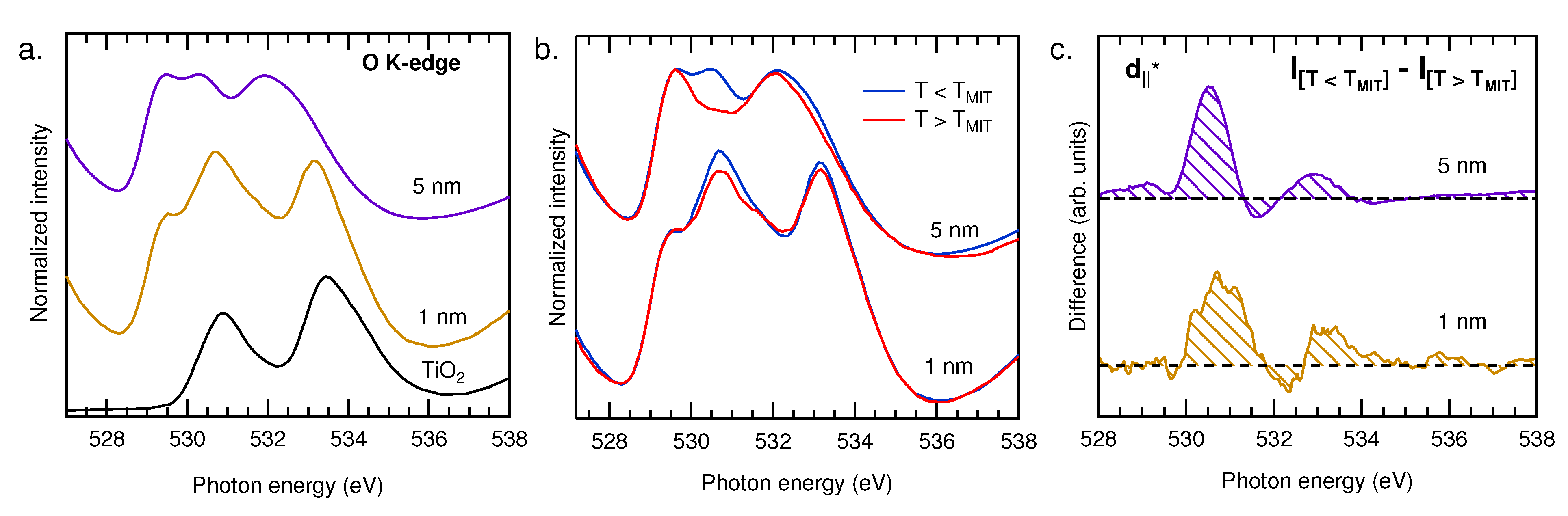
:
1. Introduction
2. Experimental Section
3. Results and Discussion
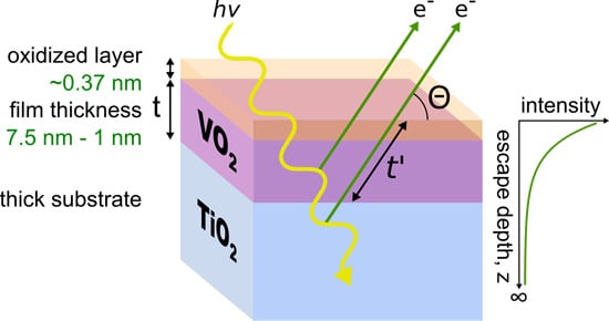
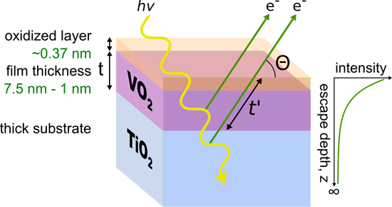
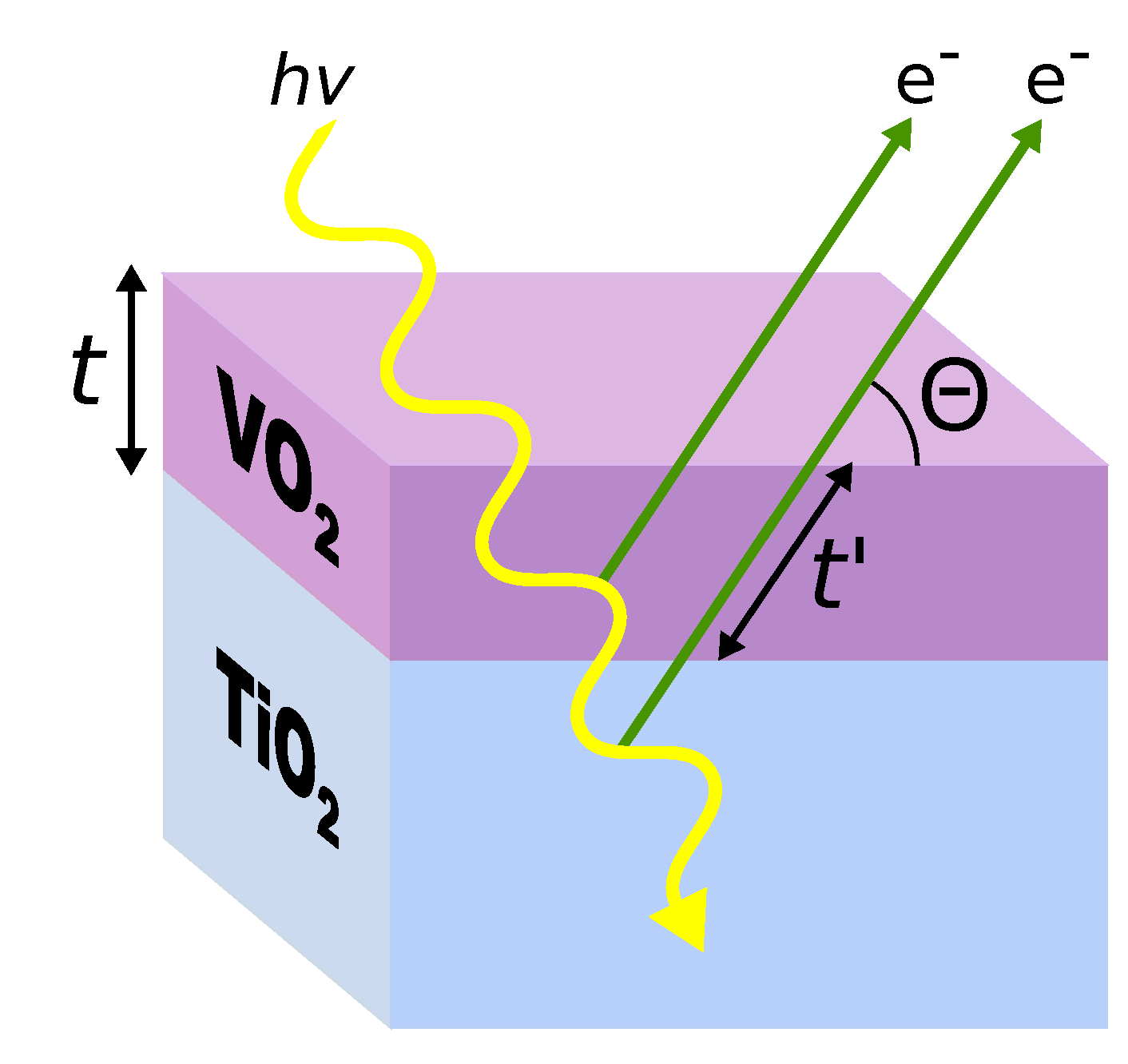
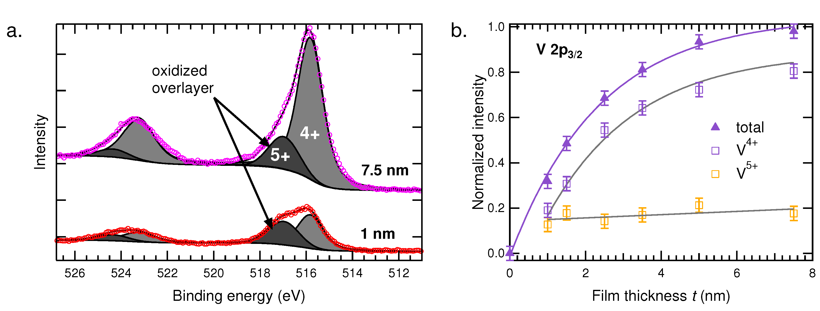
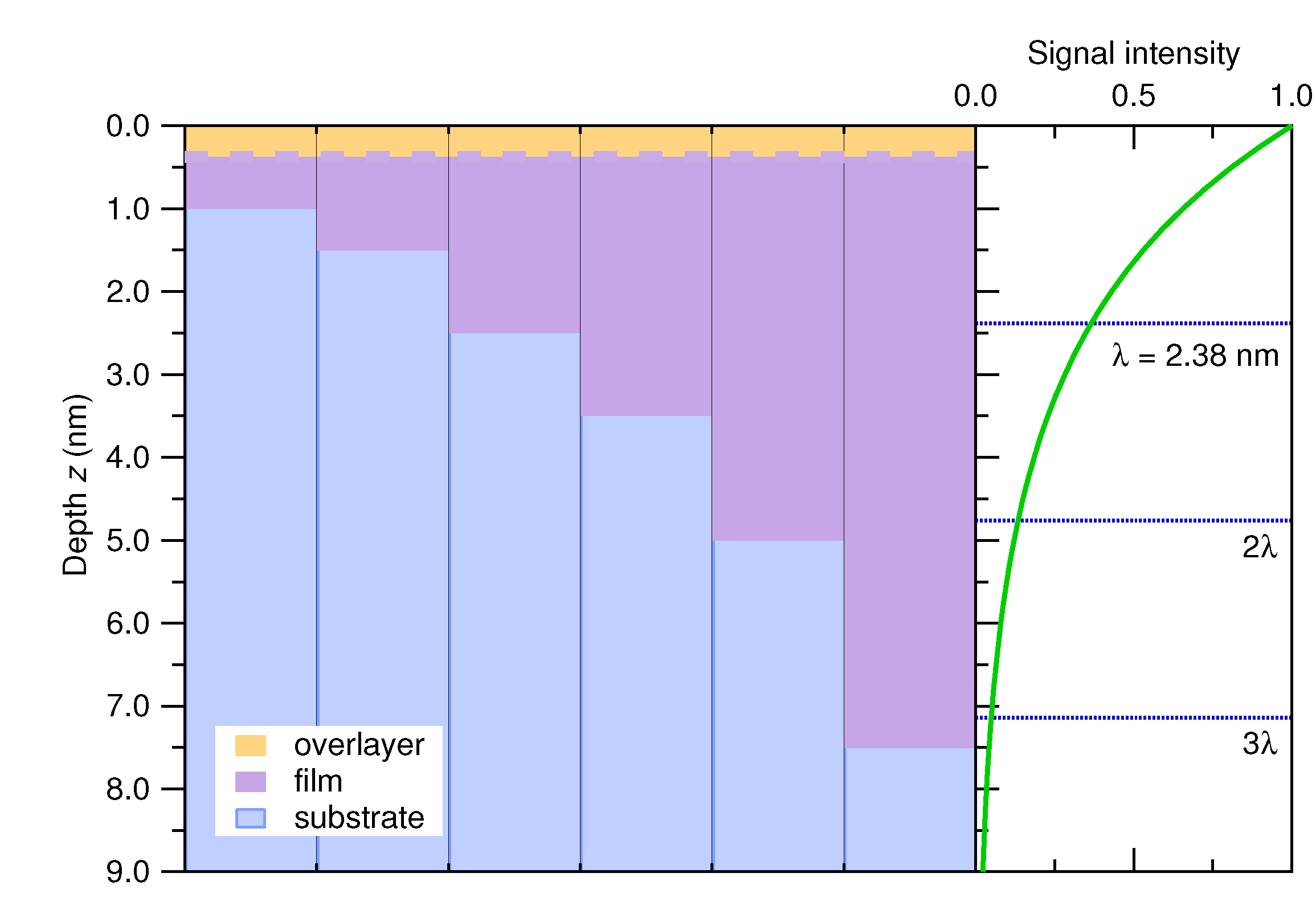
3.1. Probing Depth
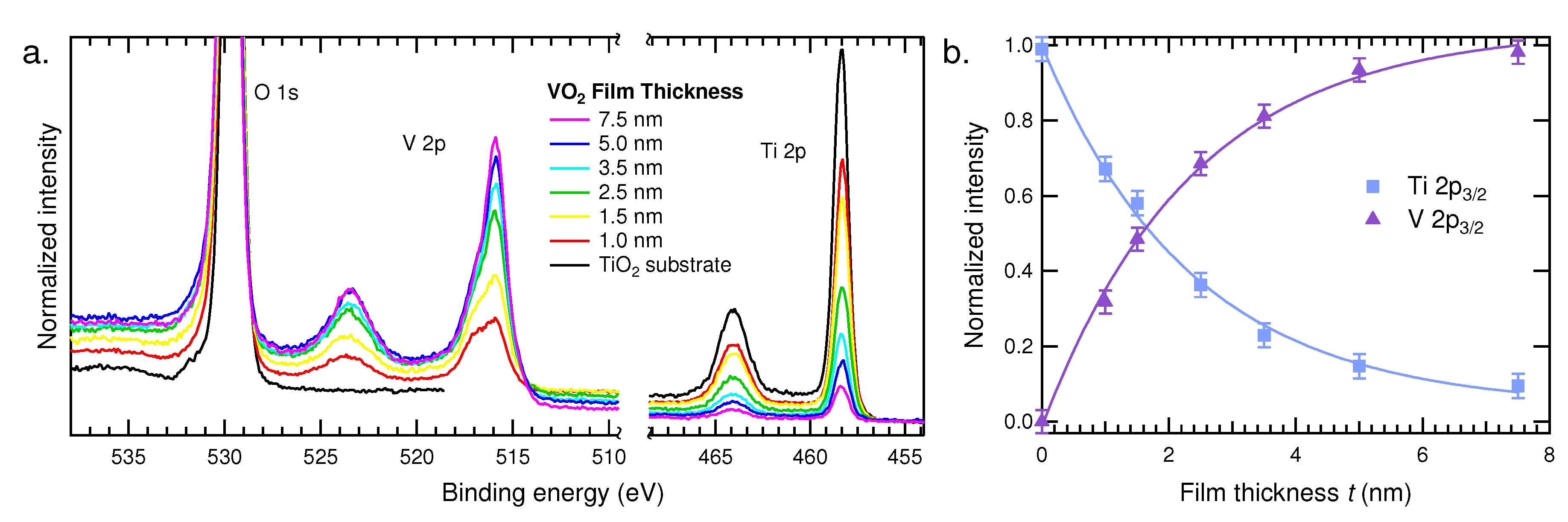
3.1.1. HAXPES


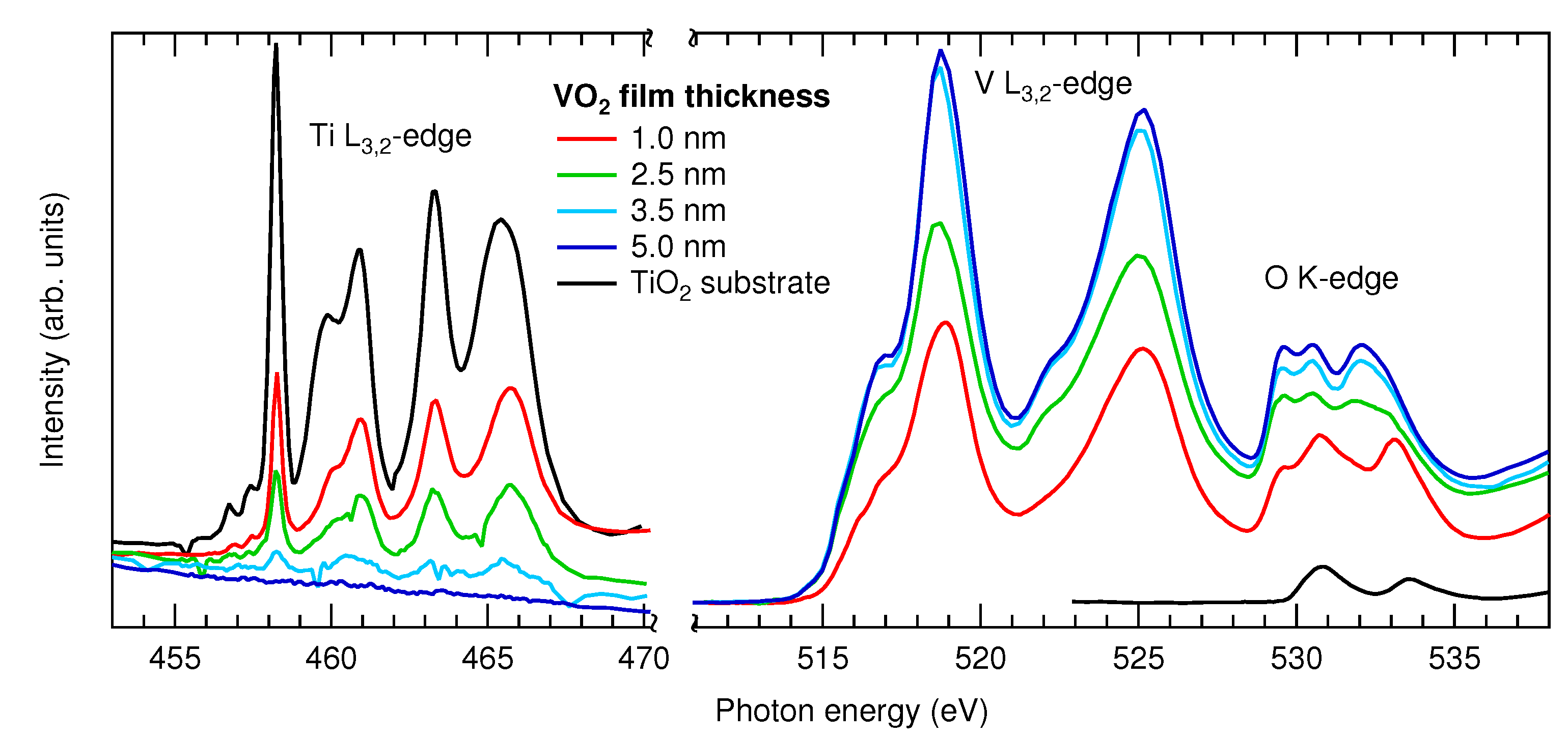
3.1.2. XAS

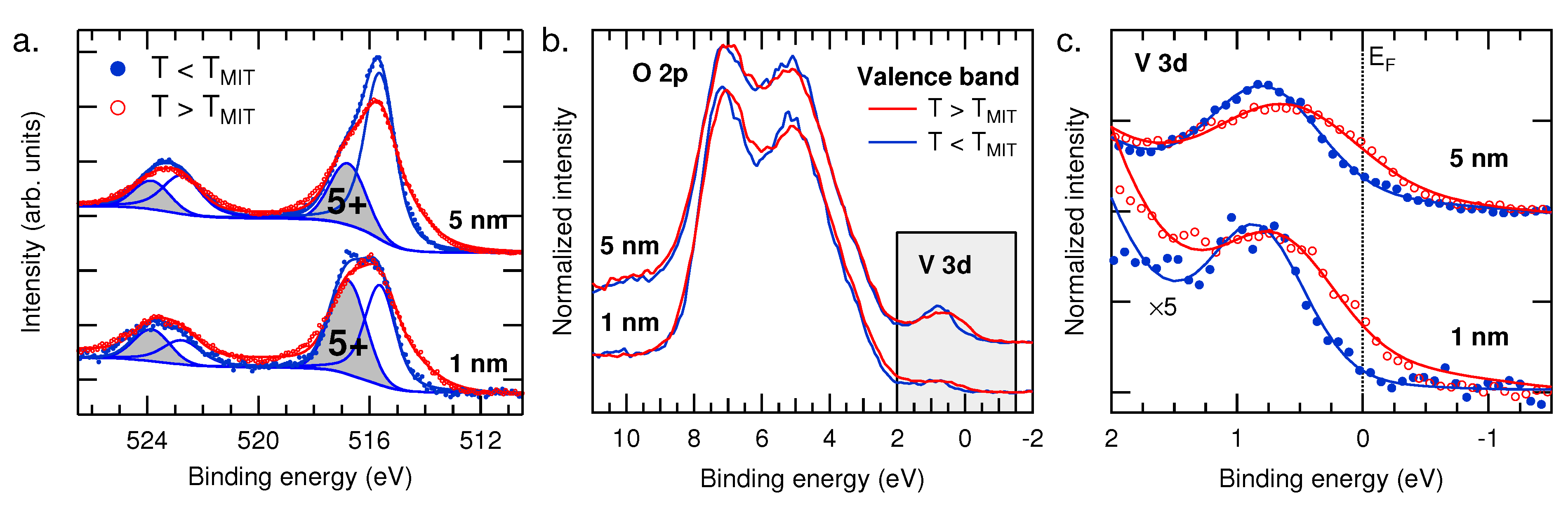
3.2. Temperature-Dependent Electronic Structure


4. Conclusions
Acknowledgments
Author Contributions
Conflicts of Interest
References
- Mannhart, J.; Schlom, D.G. Oxide interfaces—An opportunity for electronics. Science 2010, 327, 1607–1611. [Google Scholar] [CrossRef] [PubMed]
- Takagi, H.; Hwang, H.Y. An emergent change of phase for electronics. Science 2010, 327, 1601–1602. [Google Scholar] [CrossRef] [PubMed]
- Chambers, S.A. Epitaxial growth and properties of doped transition metal and complex oxide films. Adv. Mater. 2010, 22, 219–248. [Google Scholar] [CrossRef] [PubMed]
- Harrison, W.A. Electronic Structure and the Properties of Solids: The Physics of the Chemical Bond; Dover Books on Physics; Dover Publications: New York, NY, USA, 2012. [Google Scholar]
- Cox, P.A. Transition Metal Oxides: An Introduction to Their Electronic Structure and Properties; The International Series of Monographs on Chemistry; OUP Oxford: Oxford, UK, 2010. [Google Scholar]
- Cao, J.; Wu, J. Strain effects in low-dimensional transition metal oxides. Mater. Sci. Eng. R Rep. 2011, 71, 35–52. [Google Scholar] [CrossRef]
- Schlom, D.G.; Chen, L.Q.; Eom, C.B.; Rabe, K.M.; Streiffer, S.K.; Triscone, J.M. Strain tuning of ferroelectric thin films. Ann. Rev. Mater. Res. 2007, 37, 589–626. [Google Scholar] [CrossRef]
- Woicik, J.C. Local structure determination in strained-layer semiconductors. Surf. Sci. Rep. 2014, 69, 38–53. [Google Scholar] [CrossRef]
- Zhou, B.Y.; Ramanathan, S. Mott Memory and Neuromorphic Devices. IEEE Proc. 2015, 103, 1–22. [Google Scholar] [CrossRef]
- Nakano, M.; Shibuya, K.; Okuyama, D.; Hatano, T.; Ono, S.; Kawasaki, M.; Iwasa, Y.; Tokura, Y. Collective bulk carrier delocalization driven by electrostatic surface charge accumulation. Nature 2012, 487, 459–462. [Google Scholar] [CrossRef] [PubMed]
- Newns, D.M.; Misewich, J.A.; Tsuei, C.C.; Gupta, A.; Scott, B.A.; Schrott, A. Mott transition field effect transistor. Appl. Phys. Lett. 1998, 73, 780–782. [Google Scholar] [CrossRef]
- Pergament, A.L.; Stefanovich, G.B.; Velichko, A.A. Oxide Electronics and Vanadium Dioxide Perspective : A Review. J. Sel. Top. Nano Electron. Comput. 2013, 1, 24–43. [Google Scholar] [CrossRef]
- Huang, Z.; Chen, S.; Lv, C.; Huang, Y.; Lai, J. Infrared characteristics of VO2 thin films for smart window and laser protection applications. Appl. Phys. Lett. 2012, 101, 1–5. [Google Scholar] [CrossRef]
- Kats, M.A.; Sharma, D.; Lin, J.; Genevet, P.; Blanchard, R.; Yang, Z.; Qazilbash, M.M.; Basov, D.N.; Ramanathan, S.; Capasso, F. Ultra-thin perfect absorber employing a tunable phase change material. Appl. Phys. Lett. 2012, 101. [Google Scholar] [CrossRef]
- Kim, B.J.; Lee, Y.W.; Chae, B.G.; Yun, S.J.; Oh, S.Y.; Kim, H.T.; Lim, Y.S. Temperature dependence of the first-order metal-insulator transition in VO2 and programmable critical temperature sensor. Appl. Phys. Lett. 2007, 90, 2005–2008. [Google Scholar]
- Strelcov, E.; Lilach, Y.; Kolmakov, A. Gas sensor based on metal-insulator transition in VO2 nanowire thermistor. Nano Lett. 2009, 9, 2322–2326. [Google Scholar] [CrossRef] [PubMed]
- Baik, J.M.; Kim, M.H.; Larson, C.; Yavuz, C.T.; Stucky, G.D.; Wodtke, A.M.; Moskovits, M. Pd-sensitized single vanadium oxide nanowires: Highly responsive hydrogen sensing based on the metal-insulator transition. Nano Lett. 2009, 9, 3980–3984. [Google Scholar] [CrossRef] [PubMed]
- Tomczak, J.M.; Biermann, S. Optical properties of correlated materials—Or why intelligent windows may look dirty. Phys. Status Solidi Basic Res. 2009, 246. [Google Scholar] [CrossRef]
- Yang, Z.; Ko, C.; Ramanathan, S. Oxide electronics utilizing ultrafast metal-insulator transitions. Ann. Rev. Mater. Res. 2011, 41, 337–367. [Google Scholar] [CrossRef]
- Morin, F.J. Oxides which show a metal-to-insulator transition at the neel temperature. Phys. Rev. Lett. 1959, 3, 34–36. [Google Scholar] [CrossRef]
- Goodenough, J.B. The two components of the crystallographic transition in VO2. J. Solid State Chem. 1971, 3, 490–500. [Google Scholar] [CrossRef]
- Marezio, M.; McWhan, D.B.; Remeika, J.P.; Dernier, P.D. Structural aspects of the metal-insulator transitions in Cr-doped VO2. Phys. Rev. B 1972, 5, 2541–2551. [Google Scholar] [CrossRef]
- Pouget, J.P.; Launois, H.; D’Haenens, J.P.; Merenda, P.; Rice, T.M. Electron localization induced by uniaxial stress in pure VO2. Phys. Rev. Lett. 1975, 35, 873–875. [Google Scholar] [CrossRef]
- Stefanovich, G.; Pergament, A.; Stefanovich, D. Electrical switching and Mott transition in VO2. J. Phys. Condens. Matter 2000, 12, 8837–8845. [Google Scholar] [CrossRef]
- Stoliar, P.; Rozenberg, M.; Janod, E.; Corraze, B.; Tranchant, J.; Cario, L. Nonthermal and purely electronic resistive switching in a Mott memory. Phys. Rev. B 2014, 90, 1–6. [Google Scholar] [CrossRef]
- Muraoka, Y.; Hiroi, Z. Metal-insulator transition of VO2 thin films grown on TiO2 (001) and (110) substrates. Appl. Phys. Lett. 2002, 80, 583–585. [Google Scholar] [CrossRef]
- Lazarovits, B.; Kim, K.; Haule, K.; Kotliar, G. Effects of strain on the electronic structure of VO2. Phys. Rev. B 2010, 81, 1–9. [Google Scholar] [CrossRef]
- Eyert, V. The metal-insulator transitions of VO2: A band theoretical approach. Ann. Phys. 2002, 11, 650–702. [Google Scholar] [CrossRef]
- Koethe, T.C.; Hu, Z.; Haverkort, M.W.; Schüß ler Langeheine, C.; Venturini, F.; Brookes, N.B.; Tjernberg, O.; Reichelt, W.; Hsieh, H.H.; Lin, H.J.; et al. Transfer of spectral weight and symmetry across the metal-insulator transition in VO2. Phys. Rev. Lett. 2006, 97, 1–4. [Google Scholar] [CrossRef]
- Haverkort, M.W.; Hu, Z.; Tanaka, A.; Reichelt, W.; Streltsov, S.V.; Korotin, M.A.; Anisimov, V.I.; Hsieh, H.H.; Lin, H.J.; Chen, C.T.; et al. Orbital-assisted metal-insulator transition in VO2. Phys. Rev. Lett. 2005, 95, 4–7. [Google Scholar] [CrossRef]
- Laverock, J.; Preston, A.R.H.; Newby, D.; Smith, K.E.; Sallis, S.; Piper, L.F.J.; Kittiwatanakul, S.; Lu, J.W.; Wolf, S.A.; Leandersson, M.; et al. Photoemission evidence for crossover from Peierls-like to Mott-like transition in highly strained VO2. Phys. Rev. B 2012, 86, 1–5. [Google Scholar] [CrossRef]
- Cao, J.; Gu, Y.; Fan, W.; Chen, L.Q.; Ogletree, D.F.; Chen, K.; Tamura, N.; Kunz, M.; Barrett, C.; Seidel, J.; et al. Extended mapping and exploration of the vanadium dioxide stress-temperature phase diagram. Nano Lett. 2010, 10, 2667–2673. [Google Scholar] [CrossRef] [PubMed]
- Atkin, J.M.; Berweger, S.; Chavez, E.K.; Raschke, M.B.; Cao, J.; Fan, W.; Wu, J. Strain and temperature dependence of the insulating phases of VO2 near the metal-insulator transition. Phys. Rev. B 2012, 85, 1–4. [Google Scholar] [CrossRef]
- Park, J.H.; Coy, J.M.; Kasirga, T.S.; Huang, C.; Fei, Z.; Hunter, S.; Cobden, D.H. Measurement of a solid-state triple point at the metal-insulator transition in VO2. Nature 2013, 500, 431–434. [Google Scholar] [CrossRef] [PubMed]
- De Groot, F.M.F.; Grioni, M.; Fuggle, J.C.; Ghijsen, J.; Sawatzky, G.A.; Petersen, H. Oxygen 1s X-ray-absorption edges of transition-metal oxides. Phys. Rev. B 1989, 40, 5715–5723. [Google Scholar] [CrossRef]
- Van Elp, J.; Wieland, J.L.; Eskes, H.; Kuiper, P.; Sawatzky, G.A.; de Groot, F.M.F.; Turner, T.S. Electronic structure of CoO, Li-doped CoO, and LiCoO2. Phys. Rev. B 1991, 44, 6090–6103. [Google Scholar] [CrossRef]
- Chen, C.; Sette, F.; Ma, Y.; Hybertsen, M.; Stechel, E.; Foulkes, W.; Schulter, M.; Cheong, S.W.; Cooper, A.; Rupp, L.; et al. Electronic states in La2−xSrxCuO4+δ probed by soft-X-ray absorption. Phys. Rev. Lett. 1991, 66, 104–107. [Google Scholar] [CrossRef] [PubMed]
- Abbate, M.; de Groot, F.M.F.; Fuggle, J.C.; Strebel, O.; Lopez, F.; Domke, M.; Kaindl, G.; Sawatzky, G.A.; Takano, M.; Takeda, Y.; et al. Controlled-valence properties of La1−xSrxFeO3 and La1−xSrxMnO3 studied by soft-X-ray absorption spectroscopy. Phys. Rev. B 1992, 46, 4511–4519. [Google Scholar] [CrossRef]
- Fujimori, A.; Hase, I.; Namatame, H.; Fujishima, Y.; Tokura, Y.; Eisaki, H.; Uchida, S.; Takegahara, K.; de Groot, F.M.F. Evolution of the spectral function in Mott-Hubbard systems with d1 configuration. Phys. Rev. Lett. 1992, 69, 1796–1799. [Google Scholar] [CrossRef] [PubMed]
- Zhang, K.H.L.; Du, Y.; Sushko, P.V.; Bowden, M.E.; Shutthanandan, V.; Sallis, S.; Piper, L.F.J.; Chambers, S.A. Hole-induced insulator-to-metal transition in La1−xSrxCrO3 epitaxial films. Phys. Rev. B 2015, 91, 1–9. [Google Scholar] [CrossRef]
- Eguchi, R.; Taguchi, M.; Matsunami, M.; Horiba, K.; Yamamoto, K.; Ishida, Y.; Chainani, A.; Takata, Y.; Yabashi, M.; Miwa, D.; et al. Photoemission evidence for a Mott-Hubbard metal-insulator transition in VO2. Phys. Rev. B 2008, 78. [Google Scholar] [CrossRef]
- Fan, L.L.; Chen, S.; Luo, Z.L.; Liu, Q.H.; Wu, Y.F.; Song, L.; Ji, D.X.; Wang, P.; Chu, W.S.; Gao, C.; et al. Strain dynamics of ultra-thin VO2 film grown on TiO2 (001) and the associated phase transition modulation. Nano Lett. 2014, 14, 4036–4043. [Google Scholar] [CrossRef] [PubMed]
- Muraoka, Y.; Saeki, K.; Eguchi, R.; Wakita, T.; Hirai, M.; Yokoya, T.; Shin, S. Spectroscopic evidence of the formation of (V,Ti)O2 solid solution in VO2 thinner films grown on TiO2 (001) substrates. J. Appl. Phys. 2011, 109. [Google Scholar] [CrossRef] [Green Version]
- Quackenbush, N.F.; Tashman, J.W.; Mundy, J.A.; Sallis, S.; Paik, H.; Misra, R.; Moyer, J.A.; Guo, J.H.; Fischer, D.A.; Woicik, J.C.; et al. Nature of the metal insulator transition in ultra-thin epitaxial vanadium dioxide. Nano Lett. 2013, 13, 4857–4861. [Google Scholar] [CrossRef] [PubMed]
- De Jong, M.; Bergenti, I.; Dediu, V.; Fahlman, M.; Marsi, M.; Taliani, C. Evidence for Mn2+ ions at surfaces of La0.7Sr0.3MnO3 thin films. Phys. Rev. B 2005, 71, 2–5. [Google Scholar]
- Piper, L.F.J.; Preston, A.R.H.; Cho, S.W.; DeMasi, A.; Chen, B.; Laverock, J.; Smith, K.E.; Miara, L.J.; Davis, J.N.; Basu, S.N.; et al. Soft X-ray spectroscopic study of dense strontium-doped lanthanum manganite cathodes for solid oxide fuel cell applications. J. Electrochem. Soc. 2011, 158, B1523–B1531. [Google Scholar] [CrossRef]
- Dallera, C.; Braicovich, L.; Duò, L.; Palenzona, A.; Panaccione, G.; Paolicelli, G.; Cowie, B.C.C.; Zegenhagen, J. Hard X-ray photoelectron spectroscopy: Sensitivity to depth, chemistry and orbital character. Nucl. Instrum. Methods Phys. Res. Sect. A Accel. Spectrom. Detect. Assoc. Equip. 2005, 547, 113–123. [Google Scholar] [CrossRef]
- Borgatti, F.; Torelli, P.; Panaccione, G. Hard X-ray photoElectron spectroscopy of transition metal oxides: Bulk compounds and device-ready metal-oxide interfaces. J. Electron Spectros. Relat. Phenom. 2015, in press. [Google Scholar] [CrossRef]
- Wadati, H.; Fujimori, A. Hard X-ray photoemission spectroscopy of transition-metal oxide thin films and interfaces. J. Electron Spectros. Relat. Phenom. 2013, 190, 222–227. [Google Scholar] [CrossRef]
- Conti, G.; Kaiser, A.M.; Gray, A.X.; NemsÌŇaÌĄk, S.; PaÌĄlsson, G.K.; Son, J.; Moetakef, P.; Janotti, A.; Bjaalie, L.; Conlon, C.S.; et al. Band offsets in complex-oxide thin films and heterostructures of SrTiO3/LaNiO3 and SrTiO3/GdTiO3 by soft and hard X-ray photoelectron spectroscopy. J. Appl. Phys. 2013, 113. [Google Scholar] [CrossRef]
- Wahila, M.J.; Lebens-Higgins, Z.W.; Quackenbush, N.F.; Nishitani, J.; Walukiewicz, W.; Glans, P.A.; Guo, J.H.; Woicik, J.C.; Yu, K.M.; Piper, L.F.J. Evidence of extreme type-III band offset at buried n-type CdO/p-type SnTe interfaces. Phys. Rev. B 2015, 91, 1–7. [Google Scholar] [CrossRef]
- Yamamoto, Y.; Nakajima, K.; Ohsawa, T.; Matsumoto, Y.; Koinuma, H. Preparation of atomically smooth TiO2 single crystal surfaces and their photochemical property. Jpn. J. Appl. Phys. 2005, 44, 511–514. [Google Scholar] [CrossRef]
- Floating-Zone Grown Crystal; CrysTec GmbH: Berlin, Germany, 2002.
- Paik, H.; Moyer, J.A.; Spila, T.; Tashman, J.W.; Mundy, J.A.; Shukla, N.; Lapano, J.M.; Engel-herbert, R.; Zander, W.; Muller, D.A.; Datta, S.; Schiffer, P.; Schlom, D.G. Transport properties of ultra-thin VO2 films on (001) TiO2 grown by reactive molecular-beam epitaxy. Appl. Phys. Lett. 2015. submitted. [Google Scholar]
- Paik, H.; Moyer, J.A.; Tashman, J.W.; Jerry, M.; Shukla, N.; Zander, W.; Schubert, J.; Engel-Herbert, R.; Datta, S.; Schiffer, P.; et al. Thickness and orientation dependent transport property of ultra-thin VO2 films grown on TiO2 (101), (100), (111), and (110) by molecular-beam epitaxy. 2015. to be submitted. [Google Scholar]
- Silversmit, G.; Depla, D.; Poelman, H.; Marin, G.B.; de Gryse, R. Determination of the V 2p XPS binding energies for different vanadium oxidation states (V5+ to V0+). J. Electron Spectros. Relat. Phenom. 2004, 135, 167–175. [Google Scholar] [CrossRef]
- Briggs, D.; Seah, P. Practical Surface Analysis, Auger and X-ray Photoelectron Spectroscopy; Practical Surface Analysis; Wiley: Hoboken, NJ, USA, 1990. [Google Scholar]
- Cai, N.; Zhou, G.; Müller, K.; Starr, D.E. Tuning the limiting thickness of a thin oxide layer on Al(111) with oxygen gas pressure. Phys. Rev. Lett. 2011, 107, 1–4. [Google Scholar] [CrossRef]
- Stöhr, J. NEXAFS Spectroscopy; Springer Series in Surface Sciences; Springer: Berlin/Heidelberg, Germany, 2013. [Google Scholar]
- Pardo, V.; Pickett, W.E. Half-metallic semi-dirac-point generated by quantum confinement in TiO2/VO2 nanostructures. Phys. Rev. Lett. 2009, 102, 2–5. [Google Scholar] [CrossRef]
- Yao, T.; Liu, L.; Xiao, C.; Zhang, X.; Liu, Q.; Wei, S.; Xie, Y. Ultrathin nanosheets of half-metallic monoclinic vanadium dioxide with a thermally induced phase transition. Angew. Chem. Int. Ed. 2013, 52, 7554–7558. [Google Scholar] [CrossRef] [PubMed]
© 2015 by the authors; licensee MDPI, Basel, Switzerland. This article is an open access article distributed under the terms and conditions of the Creative Commons Attribution license (http://creativecommons.org/licenses/by/4.0/).
Share and Cite
Quackenbush, N.F.; Paik, H.; Woicik, J.C.; Arena, D.A.; Schlom, D.G.; Piper, L.F.J. X-Ray Spectroscopy of Ultra-Thin Oxide/Oxide Heteroepitaxial Films: A Case Study of Single-Nanometer VO2/TiO2. Materials 2015, 8, 5452-5466. https://doi.org/10.3390/ma8085255
Quackenbush NF, Paik H, Woicik JC, Arena DA, Schlom DG, Piper LFJ. X-Ray Spectroscopy of Ultra-Thin Oxide/Oxide Heteroepitaxial Films: A Case Study of Single-Nanometer VO2/TiO2. Materials. 2015; 8(8):5452-5466. https://doi.org/10.3390/ma8085255
Chicago/Turabian StyleQuackenbush, Nicholas F., Hanjong Paik, Joseph C. Woicik, Dario A. Arena, Darrell G. Schlom, and Louis F. J. Piper. 2015. "X-Ray Spectroscopy of Ultra-Thin Oxide/Oxide Heteroepitaxial Films: A Case Study of Single-Nanometer VO2/TiO2" Materials 8, no. 8: 5452-5466. https://doi.org/10.3390/ma8085255