
Investigation of the InAs/GaAs Quantum Dots’ Size: Dependence on the Strain Reducing Layer’s Position

 ,
, 
Abstract
:1. Introduction
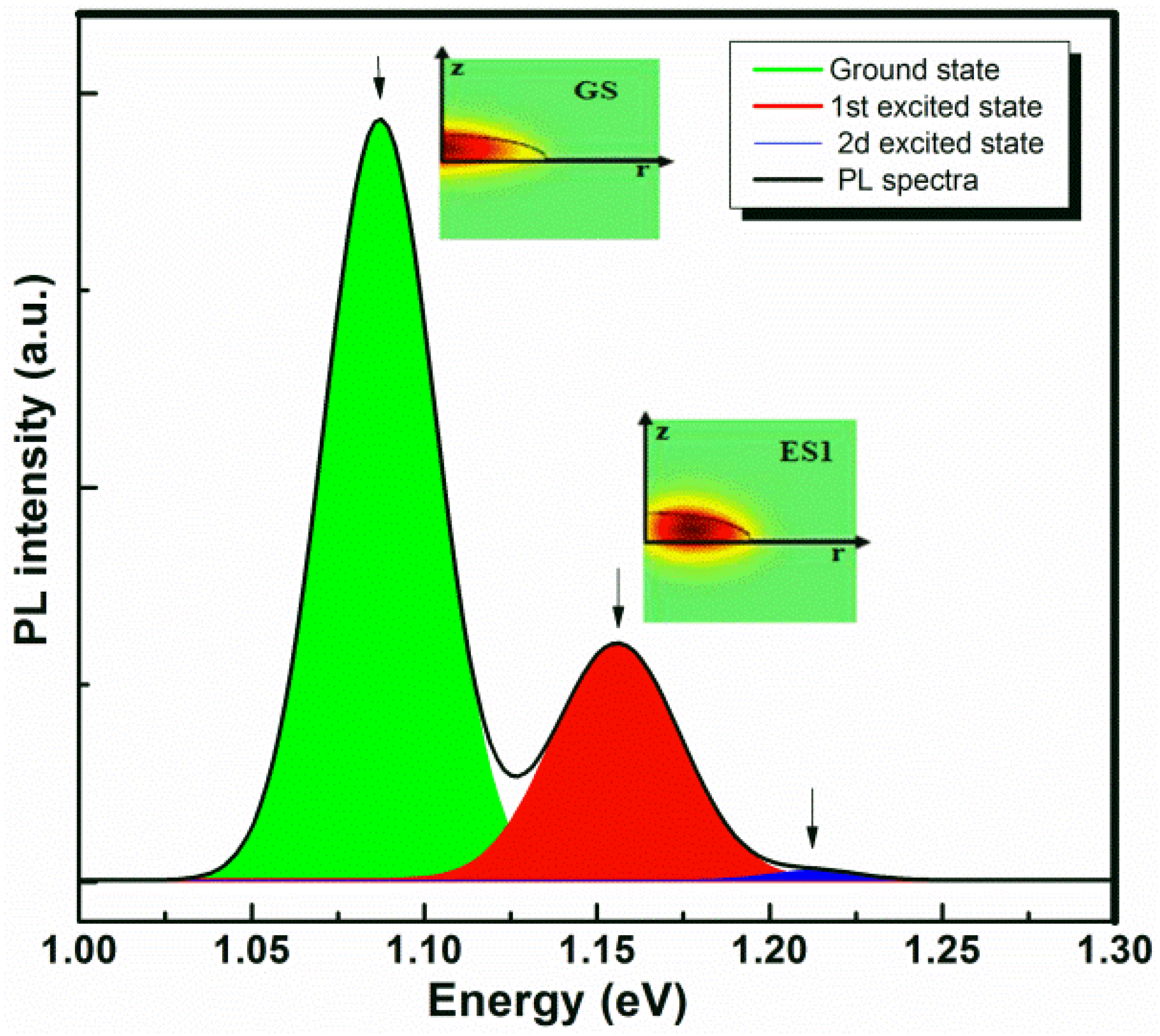
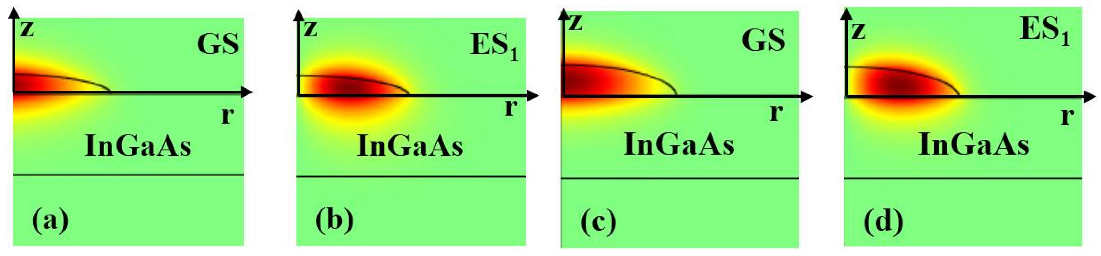
2. Results and Discussion


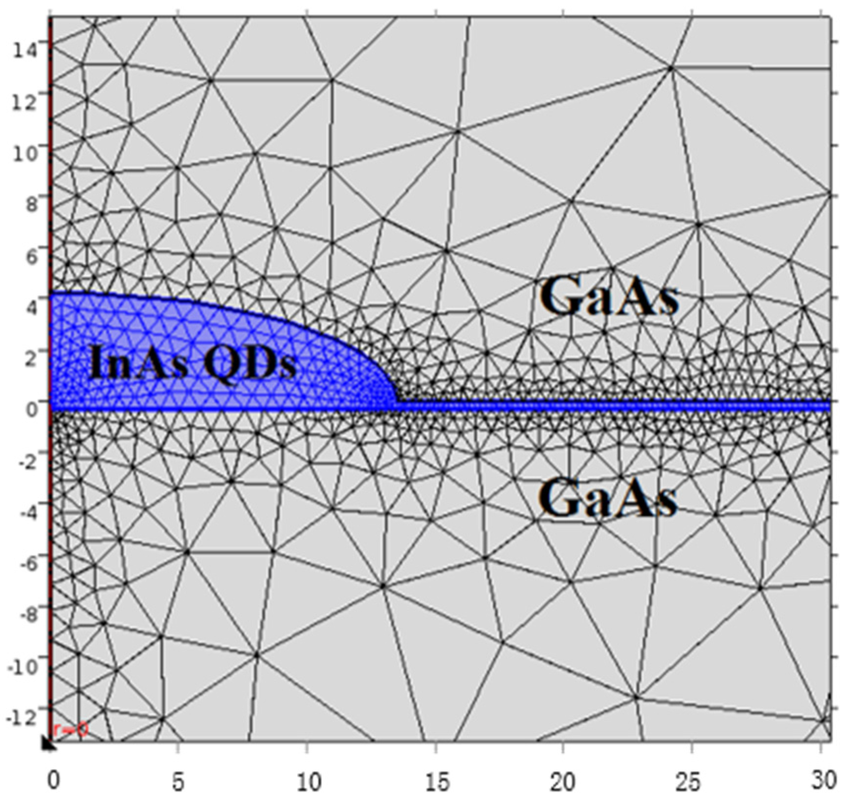
| Material | me* (m0) | mh* (m0) | C11 1011 (dyn cm−2) | C12 1011 (dyn cm−2) | ( ac−av) (eV) | b (eV) |
|---|---|---|---|---|---|---|
| InAs | 0.023 | 0.41 | 8.32 | 4.52 | −4.08 | −1.8 |
| GaAs | 0.068 | 0.5 | 12.21 | 5.66 | −6 | −2 |

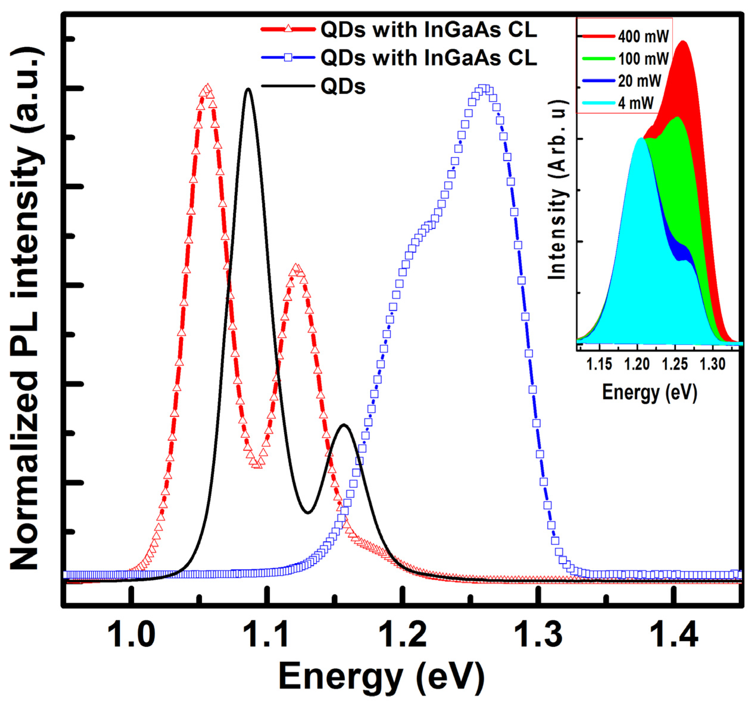
| Sample | Data | HQD/DQD | Aspect Ratio (α) | E0 (eV) | E1 (eV) | E2 (eV) |
|---|---|---|---|---|---|---|
| QDs | Experiments | 8.5/35 | 0.24 | 1.086 | 1.156 | 1.224 |
| Simulation | 3.8/28 | 0.13 | 1.083 | 1.151 | 1.238 | |
| QDCL | Experiments | 8.5/35 | 0.24 | 1.054 | 1.117 | 1.194 |
| Simulation | 4/30 | 0.13 | 1.051 | 1.113 | 1.193 | |
| Expected results | 3.8/28 | 0.13 | 1.068 | 1.131 | 1.213 | |
| QDUL | Experiments | 5/41 | 0.12 | 1.21 | 1.261 | – |
| Simulation | 2.5/29 | 0.08 | 1.204 | 1.265 | 1.331 | |
| Expected results | 3.8/28 | 0.13 | 1.071 | 1.141 | 1.217 |

3. Experimental Section
4. Conclusions
Acknowledgments
Author Contributions
Conflicts of Interest
References
- Majid, M.A.; Childs, D.T.D.; Kennedy, K.; Airey, R.; Hogg, R.A.; Clarke, E.; Spencer, P.; Murray, R. O-band excited state quantum dot bilayer lasers. App. Phys. Lett. 2011, 99, 051101. [Google Scholar]
- Ustinov, V.M.; Zhukov, A.E. GaAs-based long-wavelength lasers. Semicond. Sci. Technol. 2000, 15, 41–54. [Google Scholar]
- Salter, C.L.; Stevenson, R.M.; Farrer, I.; Nicoll, C.A.; Ritchie, D.A.; Shields, A.J. Single-photon and entangled-photon sources for quantum information. Nature 2010, 465, 594–597. [Google Scholar]
- Shields, A.J.; O’Sullivan, M.P.; Farrer, I.; Ritchie, D.A.; Hogg, R.A.; Leadbeater, M.L.; Norman, C.E.; Pepper, M. Detection of single photons using a field-effect transistor gated by a layer of quantum dots. Appl. Phys. Lett. 2000, 76, 3673–3675. [Google Scholar]
- Ledentsov, N.N. Quantum dot laser. Semicond. Sci. Technol. 2011, 26, 014001. [Google Scholar]
- Chen, J.X.; Markus, A.; Fiore, A.; Oesterle, U.; Stanley, R.P.; Carlin, J.F.; Houdré, R.; Ilegems, M.; Lazzarini, L.; Nasi, L.; et al. Tuning InAs/GaAs quantum dot properties under Stranski-Krastanov growth mode for 1.3 µm applications. J. Appl. Phys. 2002, 91, 6710–6716. [Google Scholar]
- Sogabe, T.; Shoji, Y.; Ohba, M.; Yoshida, K.; Tamaki, R.; Hong, H.F.; Wu, C.H.; Kuo, C.T.; Tomić, S.; Okada, Y. Intermediate-band dynamics of quantum dots solar cell in concentrator photovoltaic modules. Sci. Rep. 2014, 4. [Google Scholar] [CrossRef] [PubMed]
- Kong, L.; Sun, W.; Feng, Z.C.; Xie, S.; Zhou, Y.; Wang, R.; Zhang, C.; Zong, Z.; Wang, H.; Qiao, Q.; et al. Effects of InAlAs strain reducing layer on the photoluminescence properties of InAs quantum dots embedded in InGaAs/GaAs quantum wells. Thin Solid Films 2014, 562, 440–444. [Google Scholar] [CrossRef]
- Liu, H.Y.; Hopkinson, M.; Harrison, C.N.; Steer, M.J.; Frith, R.; Sellers, I.R.; Mowbray, D.J.; Skolnick, M.S. Optimizing the growth of 1.3 μm InAs/InGaAs dots-in-a-well structure. J. Appl. Phys. 2003, 93, 2931–2936. [Google Scholar] [CrossRef]
- Seravalli, L.; Minelli, M.; Frigeri, P.; Franchi, S.; Guizzetti, G.; Patrini, M.; Ciabattoni, T.; Geddo, M. Quantum dot strain engineering of InAs/InGaAs nanostructures. J. Appl. Phys. 2007, 101. [Google Scholar] [CrossRef]
- Nasr, O.; HadjAlouane, M.H.; Maaref, H.; Hassen, F.; Sfaxi, L.; Ilahi, B. Comprehensive investigation of optical and electronic properties of tunable InAs QDs optically active at O-band telecommunication window with (In)GaAs surrounding material. J. Lumin. 2014, 148, 243–248. [Google Scholar] [CrossRef]
- Ustinov, V.M.; Maleev, N.A.; Zhukov, A.E.; Kovsh, A.R.; Egorov, A.Yu.; Lunev, A.V.; Volovik, B.V.; Krestnikov, I.L.; Musikhin, Yu.G.; Bert, N.A.; et al. InAs/InGaAs quantum dot structures on GaAs substrates emitting at 1.3 μm. Appl. Phys. Lett. 1999, 74, 1384–1385. [Google Scholar]
- Nishi, K.; Saito, H.; Sugou, S.; Lee, J.S. A narrow photoluminescence linewidth of 21 meV at 1.35 μm from strain-reduced InAs quantum dots covered by In0.2Ga0.8 as grown on GaAs substrates. Appl. Phys. Lett. 1999, 74, 1111–1113. [Google Scholar]
- Pires, M.P.; Landi, S.M.; Tribuzy, C.V.B.; Nunes, L.A.; Marega, E.; Souza, P.L. InAs quantum dots over InGaAs for infrared photodetectors. J. Cryst. Growth 2004, 272, 192–197. [Google Scholar] [CrossRef]
- Chen, R.; Liu, H.Y.; Sun, H.D. Electronic energy levels and carrier dynamics in InAs/InGaAs dots-in-a-well structure investigated by optical spectroscopy. J. Appl. Phys. 2010, 107. [Google Scholar] [CrossRef]
- Joyce, P.B.; Kryzewski, T.J.; Bell, G.R.; Joens, T.S.; le Ru, E.C.; Murray, R. Optimizing the growth of 1.3 μm InAs/GaAs quantum dots. Phys. Rev. B 2001, 64, 235317. [Google Scholar] [CrossRef]
- Le Ru, E.C.; Howe, P.; Joens, T.S.; Murray, R. Strain-engineered InAs/GaAs quantum dots for long-wavelength emission. Phys. Rev. B 2003, 67, 165303. [Google Scholar]
- Nabetani, Y.; Matsumoto, T.; Sasikala, G.; Suemune, I. Theory of strain states in InAs quantum dots and dependence on their capping layers. J. Appl. Phys. 2005, 98, 063502. [Google Scholar]
- Ilahi, B.; Sfaxi, L.; Hassen, F.; Maaref, H.; Salem, B.; Guillot, G.; Jbeli, A.; Marie, X. Optical properties of 1.3 μm room temperature emitting InAs quantum dots covered by In0.4Ga0.6 As/GaAs hetero-capping layer. Appl. Phys. A 2005, 81, 813–816. [Google Scholar]
- Cherkashin, N.; Reboh, S.; Htch, M.J.; Claverie, A.; Preobrazhenskii, V.V.; Putyato, M.A.; Semyagin, B.R.; Chaldyshev, V.V. Determination of stress, strain, and elemental distribution within In(Ga)As quantum dots embedded in GaAs using advanced transmission electron microscopy. Appl. Phys. Lett. 2013, 102, 173115. [Google Scholar]
- Ilahi, B.; Sfaxi, L.; Maaref, H. Optical investigation of InGaAs-capped InAs quantum dots: Impact of the strain-driven phase separation and dependence upon post-growth thermal treatment. J. Lumin. 2007, 127, 741–746. [Google Scholar]
- Maia, A.D.B.; da Silva, E.C.F.; Quivy, A.A.; Bindilatti, V.; de Aquino, V.M.; Dias, I.F.L. Simulation of the electronic properties of InxGa1−x As quantum dots and their wetting layer under the influence of indium segregation. J. Appl. Phys. 2013, 114, 083708. [Google Scholar]
- Wang, P.; Bleloch, A.L.; Falke, M.; Goodhew, P.J.; Ng, J.; Missous, M. Direct measurement of composition of buried quantum dots using aberration-corrected scanning transmission electron microscopy. Appl. Phys. Lett. 2006, 89, 072111. [Google Scholar] [CrossRef]
- Garcı́a, J.M.; Medeiros-Ribeiro, G.; Schmidt, K.; Ngo, T.; Feng, J.L.; Lorke, A.; Kotthaus, J.; Petroff, P.M. Intermixing and shape changes during the formation of InAs self-assembled quantum dots. Appl. Phys. Lett. 1997, 74, 2014–2016. [Google Scholar] [CrossRef]
- Joyce, P.B.; Krzyzewski, T.J.; Bell, G.R.; Jones, T.S. Surface morphology evolution during the overgrowth of large InAs-GaAs quantum dots. Appl. Phys. Lett. 2001, 79, 3615–3617. [Google Scholar] [CrossRef]
- Kegel, I.; Metzger, T.H.; Lorke, A.; Peisl, J.; Stangl, J.; Bauer, G.; Nordlund, K.; Schoenfeld, W.V.; Petroff, P.M. Determination of strain fields and composition of self-organized quantum dots using x-ray diffraction. Phys. Rev. B 2001, 63, 035318. [Google Scholar]
- COMSOL Multiphysics. Available online: http://www.comsol.com (accessed on 17 July 2015).
- Vurgaftman, I.; Meyer, J.R.; Ram-Mohan, L.R. Band parameters for III–V compound semiconductors and their alloys. J. Appl. Phys. 2001, 89, 5815–5875. [Google Scholar]
- Grossi, D.F.; Smereka, P.; Keizer, J.G.; Ulloa, J.M.; Koenraad, P.M. Height control of self-assembled quantum dots by strain engineering during capping. Appl Phys. Lett. 2014, 105, 143104. [Google Scholar]
- Kim, J.S.; Yu, P.W.; Lee, J.S.; Kim, J.S.; Kim, S.G.; Leem, J.; Jeon, M. Height-controlled InAs quantum dots by using a thin InGaAs layer. Appl. Phys. Lett. 2002, 80, 4714–4716. [Google Scholar]
- Shiramine, K.; Muto, S.; Shibayama, T.; Sakaguchi, N.; Ichinose, H.; Kozaki, T.; Sato, S.; Nakata, Y.; Yokoyama, N.; Taniwaki, M. Tip artifact in atomic force microscopy observations of InAs quantum dots grown in Stranski-Krastanow mode. J. Appl. Phys. 2007, 101, 033527. [Google Scholar]
- Gong, Q.; Liang, J.B.; Xu, B.; Ding, D.; Li, H.X.; Jiang, C.; Zhou, W.; Liu, F.Q.; Wang, Z.G.; Qiu, X.H.; et al. Analysis of atomic force microscopic results of InAs islands formed by molecular beam epitaxy. J. Cryst. Growth 1998, 192, 376–380. [Google Scholar] [CrossRef]
- Simmonds, P.J.; Sun, M.; Laghumavarapu, R.B.; Liang, B.; Norman, A.G.; Luo, J.W.; Huffaker, D.L. Improved quantum dot stacking for intermediate band solar cells using strain compensation. Nanotechnology 2014, 25, 445402. [Google Scholar] [CrossRef] [PubMed]
© 2015 by the authors; licensee MDPI, Basel, Switzerland. This article is an open access article distributed under the terms and conditions of the Creative Commons Attribution license (http://creativecommons.org/licenses/by/4.0/).
Share and Cite
Souaf, M.; Baira, M.; Nasr, O.; Alouane, M.H.H.; Maaref, H.; Sfaxi, L.; Ilahi, B. Investigation of the InAs/GaAs Quantum Dots’ Size: Dependence on the Strain Reducing Layer’s Position. Materials 2015, 8, 4699-4709. https://doi.org/10.3390/ma8084699
Souaf M, Baira M, Nasr O, Alouane MHH, Maaref H, Sfaxi L, Ilahi B. Investigation of the InAs/GaAs Quantum Dots’ Size: Dependence on the Strain Reducing Layer’s Position. Materials. 2015; 8(8):4699-4709. https://doi.org/10.3390/ma8084699
Chicago/Turabian StyleSouaf, Manel, Mourad Baira, Olfa Nasr, Mohamed Helmi Hadj Alouane, Hassen Maaref, Larbi Sfaxi, and Bouraoui Ilahi. 2015. "Investigation of the InAs/GaAs Quantum Dots’ Size: Dependence on the Strain Reducing Layer’s Position" Materials 8, no. 8: 4699-4709. https://doi.org/10.3390/ma8084699