Article

Fine Structure in Multi-Phase Zr8Ni21-Zr7Ni10-Zr2Ni7 Alloy Revealed by Transmission Electron Microscope

1
BASF-Ovonic, 2983 Waterview Drive, Rochester Hills, MI 48309, USA
2
Material Measurement Laboratory, National Institute of Standards and Technology, Gaithersburg, MD 20899, USA
*
Author to whom correspondence should be addressed.
Materials 2015, 8(7), 4618-4630; https://doi.org/10.3390/ma8074618
Submission received: 27 May 2015 / Revised: 6 July 2015 / Accepted: 16 July 2015 / Published: 22 July 2015

Abstract

:
The microstructure of an annealed alloy with a Zr8Ni21 composition was studied by both scanning electron microscopy (SEM) and transmission electron microscopy (TEM). The presence of three phases, Zr8Ni21, Zr2Ni7, and Zr7Ni10, was confirmed by SEM/X-ray energy dispersive spectroscopy compositional mapping and TEM electron diffraction. Distribution of the phases and their morphology can be linked to a multi-phase structure formed by a sequence of reactions: (1) L → Zr2Ni7 + L’; (2) peritectic Zr2Ni7 + L’ → Zr2Ni7 + Zr8Ni21 + L”; (3) eutectic L” → Zr8Ni21 + Zr7Ni10. The effect of annealing at 960 °C, which was intended to convert a cast structure into a single-phase Zr8Ni21 structure, was only moderate and the resulting alloy was still multi-phased. TEM and crystallographic analysis of the Zr2Ni7 phase show a high density of planar (001) defects that were explained as low-energy boundaries between rotational variants and stacking faults. The crystallographic features arise from the pseudo-hexagonal structure of Zr2Ni7. This highly defective Zr2Ni7 phase was identified as the source of the broad X-ray diffraction peaks at around 38.4° and 44.6° when a Cu-K was used as the radiation source.

1. Introduction

Zr-based AB2 metal hydride (MH) alloys are considered as an alternative for the misch metal-based AB5 MH alloys currently used as the active material in the negative electrode of the nickel/metal hydride (Ni/MH) rechargeable batteries that are used in consumer and hybrid electric vehicle applications. The AB2 MH alloys offer higher capacities [1,2,3], higher flexibility in composition design [4,5,6,7], and are exempt from the market price volatility of rare earth metals. Beside the Laves phase-based pseudo-binary AB2, different Zr-Ni intermetallics (with or without substitution) are also of great interest for the improvement in both capacity and high-rate dischargeability (HRD) of the MH alloys. For example, ZrNi5 [8], Zr2Ni7 [9], ZrNi3 [10], Zr8Ni21 [11,12], ZrNi2 [13,14], Zr7Ni10 [15,16,17], Zr9Ni11 [18], ZrNi [19,20], and Zr2Ni [21] with different partial substitutions were studied as MH alloys for the potential application in Ni/MH batteries. Out of these Zr-Ni intermetallic alloys, Zr8Ni21 is very important since its stoichiometry is ideal for room temperature applications, such as the Ni/MH battery. It is not normally seen as a secondary phase in the multi-phase Zr-based MH alloys due to its peritectic origin in the phase diagram. The Zr8Ni21 phase is not stable and is seldom observed in partially substituted Zr8Ni19X2 alloys [11]. The undoped Zr8Ni21 shows a gas-solid storage of 0.63% mass fraction hydrogen at 30 °C and an electrochemical discharge capacity of 136 mAh·g−1 [12]. In this study, X-ray diffraction (XRD) of both as-cast and annealed (960 °C for 8 h) Zr8Ni21 samples consistently shows the presence of broad peaks around 38.4° and 44.6°, which could not be reconciled with XRD and scanning electron microscopy (SEM) results (Figure 2a,b in [11]). In the same paper, the broad peaks from XRD analysis were suspected to be a result of the fine microcrystal mixtures from the ZrNi and ZrNi5 phases found by SEM/X-ray energy dispersive spectroscopy (EDS) analysis. Similar broad peaks were also found in a paper by Ruiz and his coworkers for a Zr8Ni21 sample annealed at 1000 °C for 30 days, but were not identified [22]. Since the peaks cannot be explained by International Centre of Diffraction Data [23], and the broadness was not consistent with other peaks, the presence of one or more additional phases was suspected. Transmission Electron Microscopy (TEM) applied together with other chemical-sensitive techniques (EDS, electron energy-loss spectroscopy, etc.) is capable of providing both structural and chemical information at the sub-atomic level [24,25,26]. Crystal structure, chemical composition, or atomic bonding can be easily characterized [27,28,29]. In this paper, we investigated the same alloy by advanced TEM technique with the goal to identify the origin of the broad peaks and find the suspected minor phase(s). The full understanding of the phase components in the Zr8Ni21 base alloy is very important for the future development of multi-phase Zr-based MH alloy with various substitutions for electrochemical applications.

2. Experimental Section

The ingot sample was prepared by arc melting 10 g of Zr and Ni mixture with the stoichiometric ratio of 8:21, respectively, under a continuous argon flow with a non-consumable tungsten electrode and a water-cooled copper tray. Before melting the Zr and Ni mixture, a piece of titanium used as oxygen getter underwent a few melting-cooling cycles to reduce the residual oxygen concentration in the system. The ingot was re-melted and flipped over a few times to ensure uniformity in chemical composition. The ingot was annealed at 960 °C for 8 h in an argon environment. The average chemical composition of the sample was examined with a Varian Liberty 100 inductively coupled plasma (ICP) system (Analytical West, Inc., Corona, CA, USA). A Rigaku Miniflex XRD (Rigaku Corporation, Tokyo, Japan) was used to study the phases of the sample. JEOL JSM7100 field emission SEM (JEOL Ltd., Tokyo, Japan) with EDS capability was used to study the sample’s microstructure and compositional distribution by collecting EDS mapping data from polished surface of the sample. For TEM measurements, samples were thinned by a mechanical polish followed by an ion milling. FEI Titan 80-300 TEM/STEM (FEI, Inc., Hillsboro, OR, USA) was used to study the microstructure of the alloy samples.

3. Results and Discussion

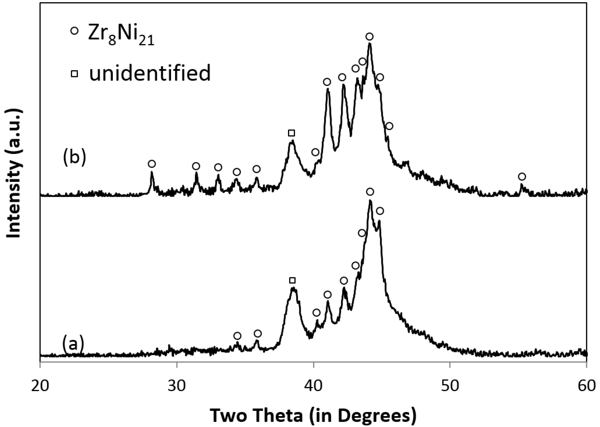
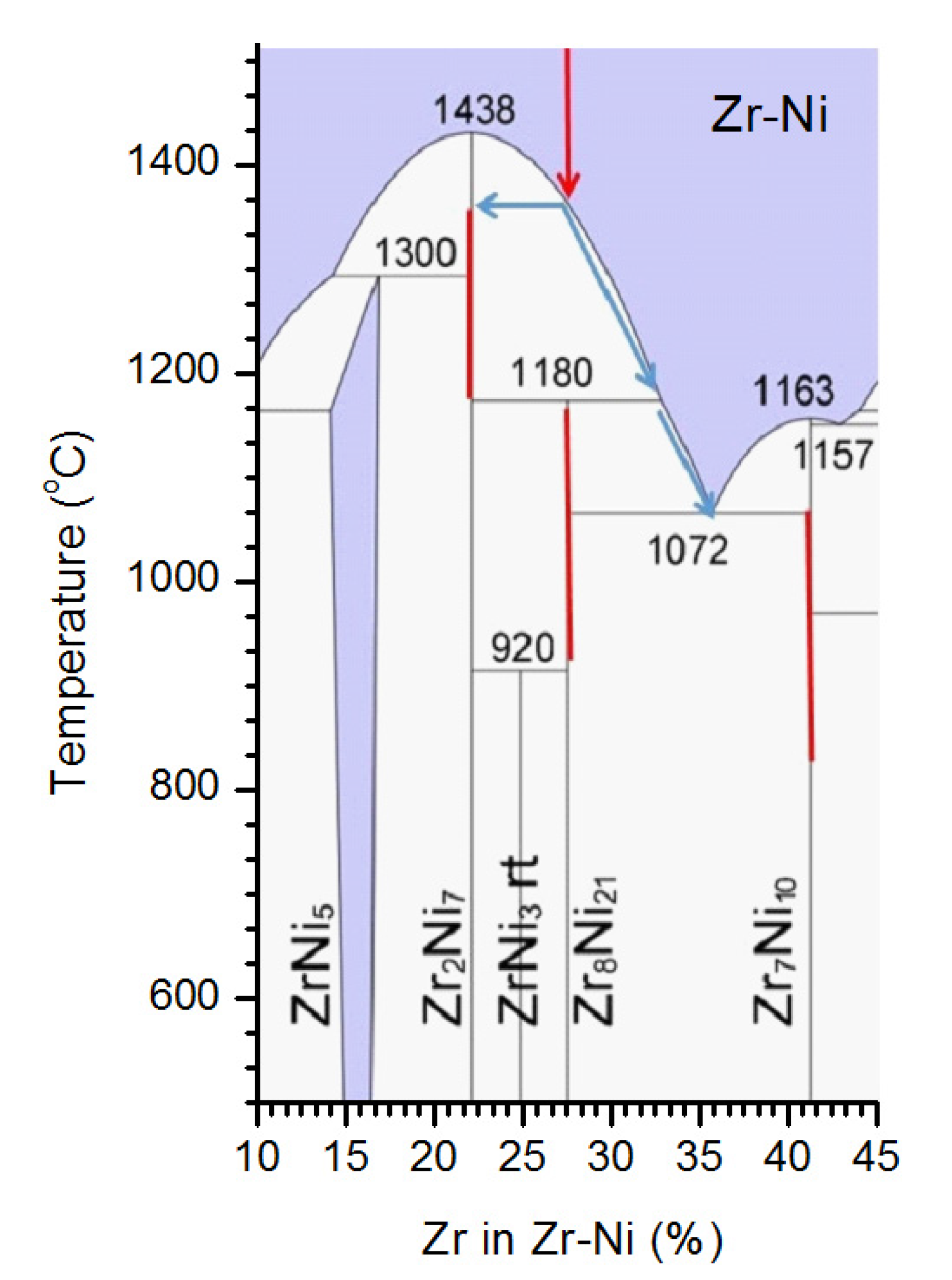
3.1. Phases, Microstructure, and Formation Path
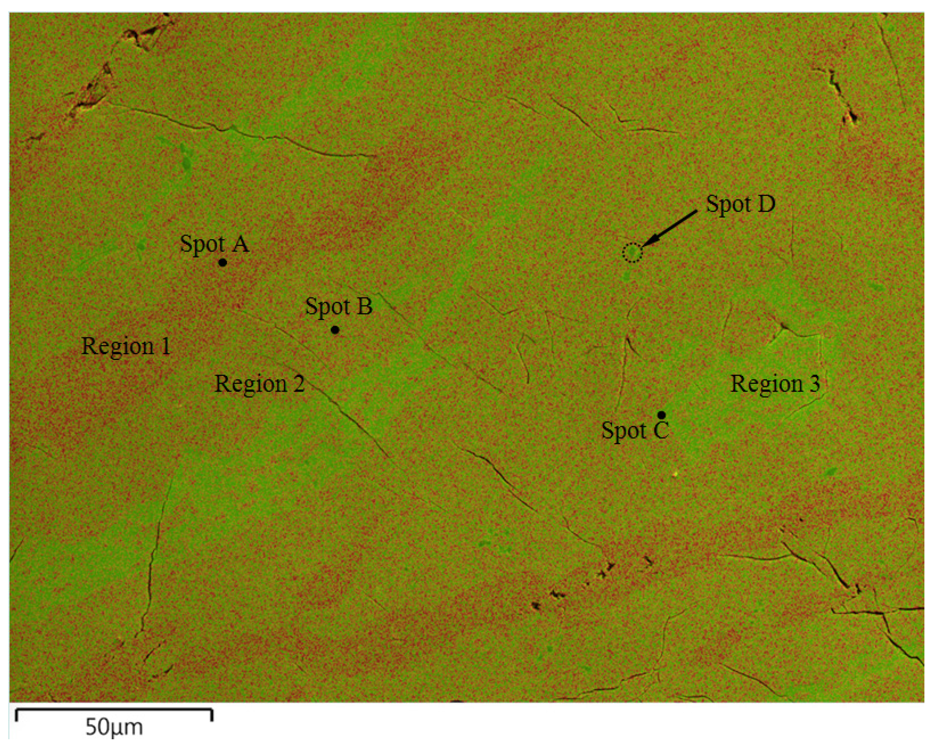
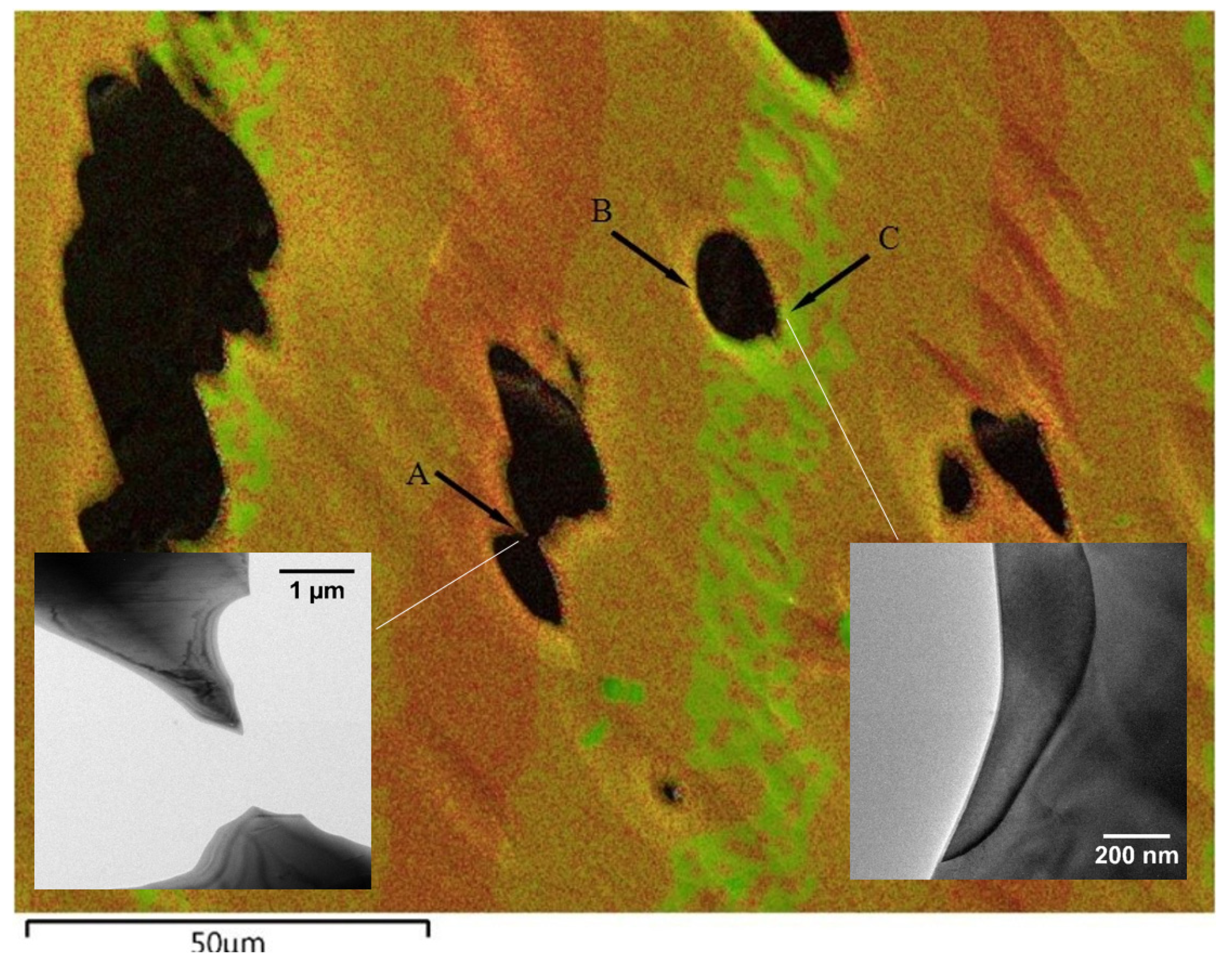
The chemical composition measurement result obtained by ICP from the annealed alloy showed that the actual atomic ratio of Zr/Ni (27.1%/72.9%) was close to the Zr8Ni21 design (27.6%/72.4%). According to the XRD measurement results from as-cast and annealed samples (Figure 1), most significant peaks were attributed to the Zr8Ni21 phase, thus indicating that Zr8Ni21 is the dominant phase of the microstructure. However, there were two broad peaks shown on the XRD pattern, e.g., at 38.4° and 44.6°, which suggested the presence of other phase(s) in addition to Zr8Ni21. In the previous paper, EDS measurements collected from different spots were used to evaluate phases of the material [11]. Based on the EDS results, it was claimed that there were three phases corresponding to the Zr8Ni21 phase, a mix of the Zr8Ni21 and ZrNi phases, and a mix of the Zr8Ni21 and ZrNi5 phases. However, the reason such mixed-phase regions presented was not clear. To verify and further study the structure, the measurements were carried out again at National Institute of Standards and Technology (NIST) with EDS mapping. A composition map of the sample is shown in Figure 2, where three colors, green, red, and gray, correspond to Zr, Ni, and the SEM secondary electron image (SEI), respectively. Quantitative EDS analysis revealed that the Ni/Zr atomic ratios of the identified phases, Regions 1, 2, and 3, are consistent with the stoichiometries close to Zr7Ni10, Zr8Ni21, and Zr2Ni7, respectively (Table 1). Occasional inclusions of ZrO2 were also found in the alloy (Spot D). These ZrO2 inclusions appear to be much lower in average atomic weight, showing darker contrast in the SEM backscattering electron image (Figure 1a in Reference [11]).
Figure 1. XRD patterns using Cu-Kα as the radiation source for Zr8N21 as-cast (a) and after an 8-h annealing at 960 °C in an Ar environment (b).
Materials 08 04618 g001
Figure 2. Integrated Zr-Lα1 EDS map (green), Ni-Kα1 EDS map (red), and SEM secondary electronic image (gray scale), showing different phases in the sample, including Region 1 (Zr2Ni7), Region 2 (Zr8Ni21, the major phase), and Region 3 (Zr7Ni10).
Materials 08 04618 g002
Table 1. Comparison between the EDS measured Ni-Zr composition ratio and the composition from the corresponding stoichiometric phase.
Phases from Figure 2EDS Zr at%EDS Ni at%Corresponding Ni-Zr phasesStoichiometric Ni at%
Spot A (Region 1)22 (±2)78 (±2)Zr2Ni777.8
Spot B (Region 2)27 (±2)73 (±2)Zr8Ni2172.7
Spot C (Region 3)40 (±2)60 (±2)Zr7Ni1058.8
Spot D93 (±2)7 (±2)
Further confirmation of the phases came from the crystallographic analysis of the phases by electron diffraction from the TEM sample. Before being examined by TEM, SEM/EDS mapping was obtained for the TEM sample, which served as a road map for TEM data collection. For example, in Figure 3, areas A, B, and C are electron-transparent thin areas and are located in a Ni-rich region, a major Zr8Ni21 phase region, and a Zr-rich region, respectively. Typical bright field TEM images taken from the thin areas are shown in the insets of Figure 3. High resolution TEM images and selected area electron diffraction (SAED) patterns were also taken from these areas, as shown in Figure 4. Indexing of the patterns and comparing with simulations [30,31,32] demonstrated that the Zr-rich phase (green color) has an orthorhombic Zr7Ni10 structure, while the phase of the highest volume fraction (orange color) has a triclinic Zr8Ni21 structure, which is consistent with SEM/EDS analysis.
Figure 3. Integrated Zr-Lα1 (green) EDS map, Ni-Kα1 (red) EDS map, and SEM secondary electronic image (gray scale) obtained from thinned regions of a TEM sample used for diffraction identification of phases.
Materials 08 04618 g003
Figure 4. High-resolution TEM images (a, c and e) and corresponding selected area diffraction patterns (b, d and f) obtained from areas A, B and C in Figure 2, respectively. With the help of single crystal diffraction simulations and indexing (red circles), the structures of areas A, B and C are identified as Zr2Ni7, Zr8Ni21 and Zr7Ni10, respectively.
Materials 08 04618 g004
Such phase distribution in this Zr-Ni alloy material can be well explained by the Zr-Ni phase diagram with the assumption that annealing of the alloy was not sufficient to eliminate the cast structure (otherwise a single-phase Zr8Ni21 structure would be observed) (Figure 5). During the casting process of the sample with a Zr8Ni21 composition, the Zr2Ni7 phase is first to crystallize from the melt during cooling down at about 1370 °C. Dendrites of Zr2Ni7 nucleate and grow until the temperature reaches 1180 °C. At this point, the peritectic reaction between solid Zr2Ni7 and liquid is attempted; the reaction results in the formation of the Zr8Ni21 phase that envelops the Zr2Ni7 dendrites. The peritectic reaction is diffusion-limited, and the continuous cooling may not allow enough time for the reaction to be completed. Thus, the remaining liquid, now enriched in Ni, experiences a eutectic reaction at a temperature below 1072 °C, which results in the formation of a two-phase mixture of Zr8Ni21 and Zr7Ni10. With this description the observed microstructure and phases are understood as: Region A, remnants of the first-to-form Zr2Ni7 phase; Region B, Zr8Ni21 formed by peritectic reaction; and Region C (of two phases), a product of eutectic reaction L → Zr8Ni21 + Zr7Ni10. Judging from its average stoichiometry (59.9% of Ni), Region C is composed of 92% Zr7Ni10 (58.8% of Ni) and 8% Zr8Ni21 (72.7% of Ni).
Figure 5. Ni-Zr phase diagram showing formation of the observed phases during continuous cooling of the Zr8Ni21 melt.
Materials 08 04618 g005

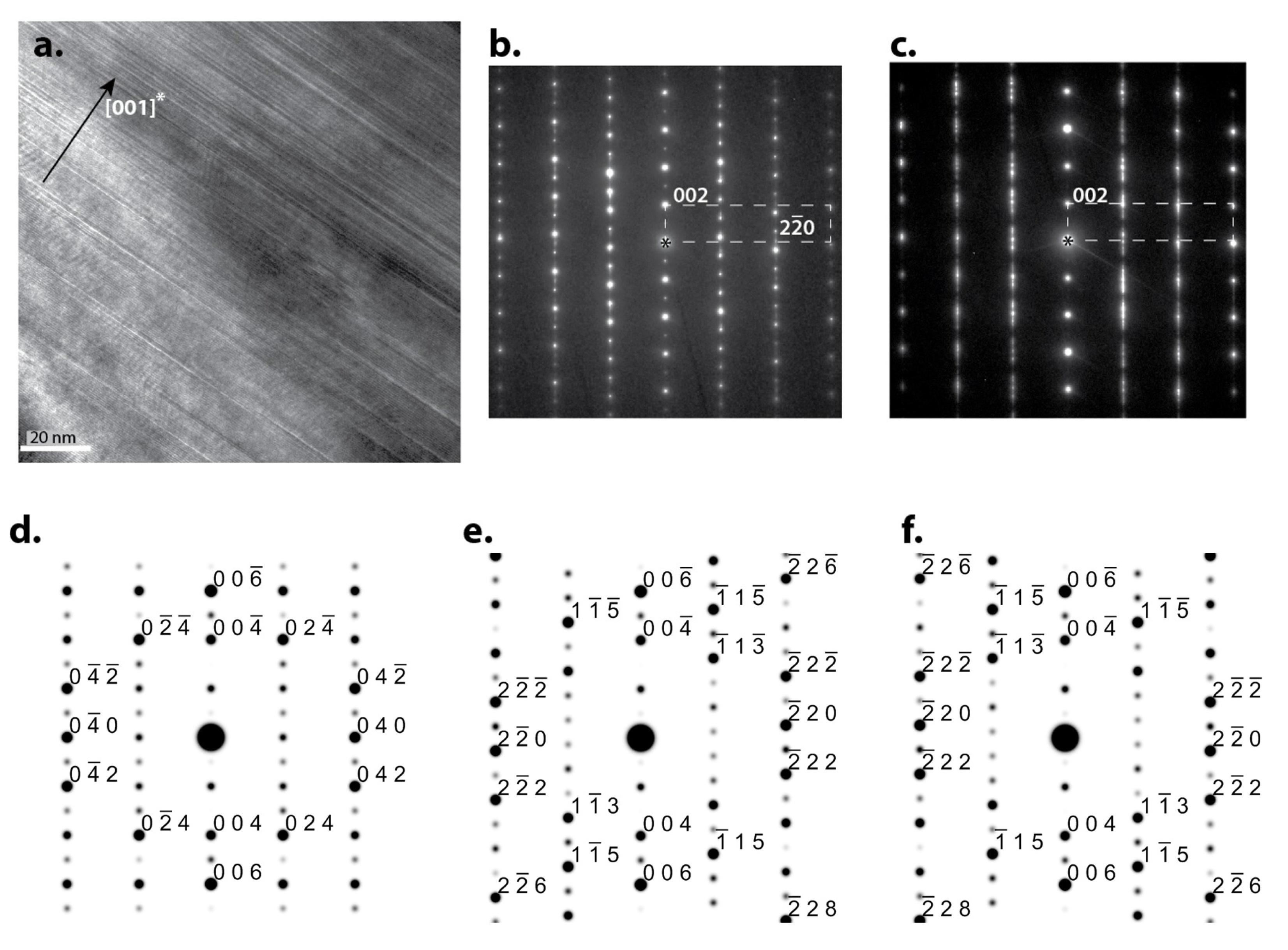
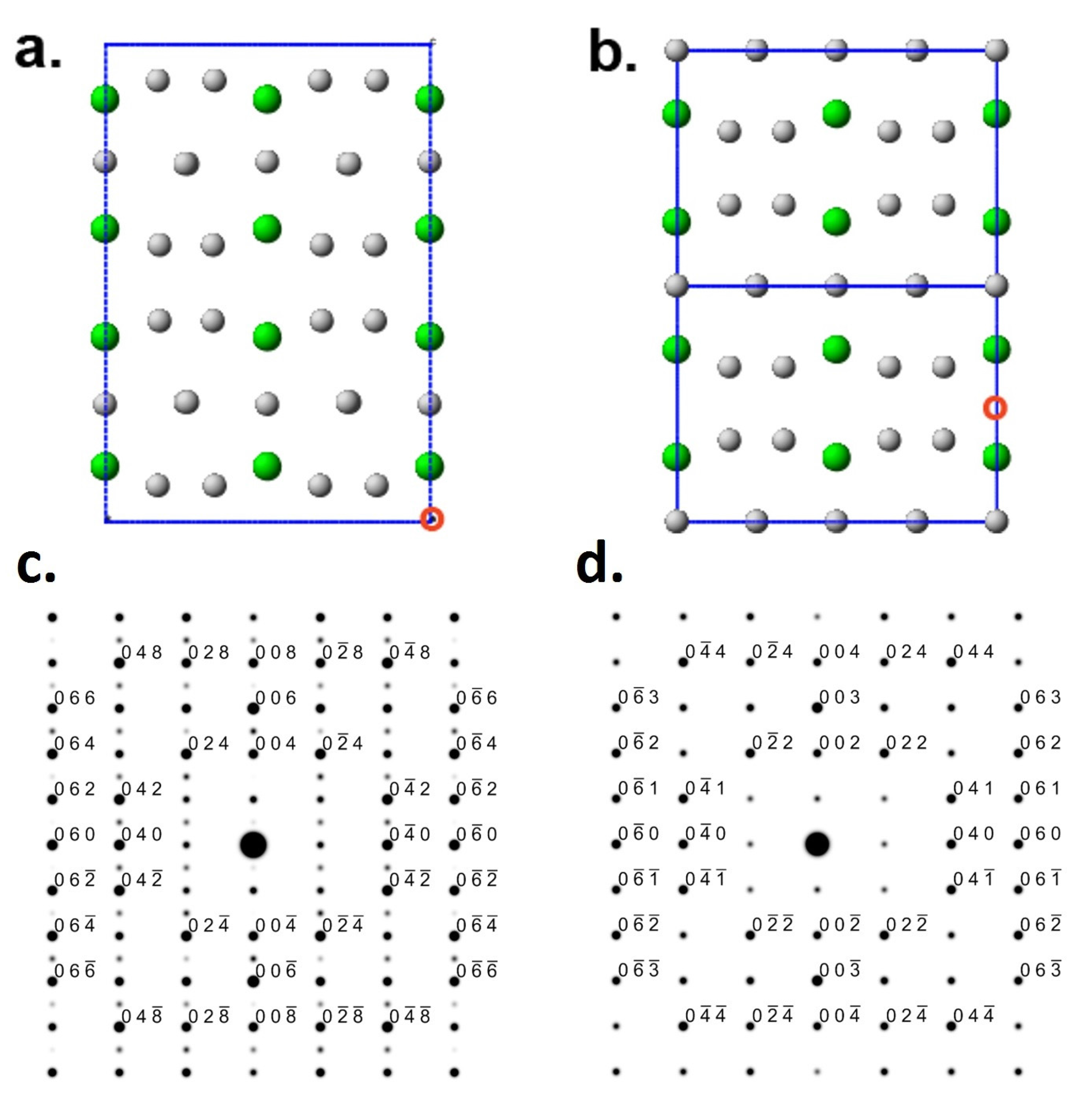
3.2. Defects and Crystallography of the Zr2Ni7 Phase

While a good agreement among EDS/SEM/TEM measurements and the Ni-Zr phase diagram was established, certain unreported structural features of the Zr2Ni7 phase have warranted further TEM investigation. Figure 6a shows the bright field image from the region identified by EDS as the Zr2Ni7 phase. The image shows a high density of planar defects according to SAED patterns. Figure 6b,c indicate the defect planes are (001) of Zr2Ni7. A SAED pattern forms a region with a lower density of defects in Figure 6b and shows that it can be indexed as Zr2Ni7 in the [110] zone axis, which is confirmed by comparing it with the simulated [110] patterns, Figure 6e, using a structural model of Eshelman et al. [24]. However, SAED from regions with a higher density of defects, Figure 6b, shows a dense distribution of reflection and intensity streaks along the 0 kl rows. The reflections can be explained by the overlapping of SAED patterns from three orientations of Zr2Ni7, [100], [110], and [ 11 ¯ 0]; the simulated SAED patterns of these zone axes are shown in Figure 6d–f. From this analysis the observed planar defects can be interpreted as interfaces between 60° rotational (around [001]*) domains of Zr2Ni7, as well as stacking faults that interrupt the long range ordering sequence.
Figure 6. Bright field TEM micrograph of the Zr2Ni7 phase showing parallel planar defects (a) and corresponding SAED patterns (b,c) showing that the defects’ plane is (001) of the Zr2Ni7 phase with the simulated diffraction patterns along [100] (d), [110] (e) and [ 11 ¯ 0 ] (f) directions.
Materials 08 04618 g006
The reason for the copious formation of these rotational domains is the pseudo-hexagonal nature of the monoclinic Zr2Ni7 structure. Figure 7a shows a projection of the structure in the [100] direction; the structure can be described as a stacking of two types of layers with compositions of Ni2Zr and Ni3. The structure can be subdivided into two very similar blocks consisting of two Ni2Zr and one Ni3 layers. Figure 7b,c show projections of the layers with an outlined two-dimensional unit cell, from which the pseudo-hexagonal close-packed arrangement of atoms is evident. The hexagonal nature of the layers is not clear from the usual SAED taken with the electron beam’s direction normal to the layers’ planes (ZA = [0.24 0 0.9]) as shown in Figure 7d, but when simulations are done for very thin crystal that allow intersection of intensity rows with the Ewald sphere, the pseudo-hexagonal symmetry becomes evident (Figure 7e). However, the Ni2Zr layers, which have identical structural projections, are subdivided into two variants differentiated by the deviation of Zr and Ni from the medial plane: L1 and L4 with Zr upward and L3 and L6 with Ni upward (Figure 7a).
Figure 7. A projection of the Zr2Ni7 structure in the [100] direction (a), projections of the layers from (a) with an outlined pseudo-hexagonal unit cell (b,c) and simulated SAED patterns with the electron beam’s direction normal to the layers’ planes (ZA = [0.24 0 0.9]) for very thin (1 nm) (d) and thicker (10 nm) (e) Zr2Ni7 crystals.
Materials 08 04618 g007
Due to the close-packed (CP) arrangement of atoms within the layers, there are three CP positions, α, β, and γ, for the hard-sphere close-packed staking of these layers in the direction normal to the layers’ planes. In the Zr2Ni7 structure, the layers within a block are in the same CP position (e.g., α for Block 1), but the blocks are shifted to the next CP position (e.g., β for Block 2). Thus, the Zr2Ni7 structure can be described as the following sequence: Ni2Zr(α)-Ni3(α)-Ni2Zr’(α)-Ni2Zr(β)-Ni3(β)-Ni2Zr’(β). Mistakes in 60° rotation of the pseudo-hexagonal layer change the direction of the distortion result in a monoclinic rotational variant with low-energy interdomain (001) interface. Mistakes in the selection of CP position (e.g., γ instead of β) lead to the formation of low-energy staking faults.
SAED patterns in Figure 6b,c show a significant difference in the intensity of (00l) reflections with odd l; in some samples' locations, the (00l) reflections are completely lacking. These variations can be understood as the following: according to the structural model of Eshelman [24], the structural blocks shown in Figure 7a are very similar but not identical, thus the periodicity c = 1.2193 nm. In the analysis by Parthe and Lemair [33], by allowing small changes in the point positions of less than 0.5 nm, a unit-cell transformation can be made which leads to a smaller monoclinic unit cell with c = 0.6307 nm. In this structure, Blocks 1 and 2 are identical (Figure 8a,b), but the diffraction is lacking odd (00l), or (002) become a new structure (001) (Figure 8c,d).
Figure 8. Projection of the Zr2Ni7 structure in the [100] direction for a structural model of Eshelman [24] and Parthe [27] (a), a projection of the layers from (a) with an outlined pseudo-hexagonal unit cell (b) and simulated SAED patterns with the electron beam’s direction normal to the layers’ planes (ZA = [0.24 0 0.9]) for very thin (1 nm) (c) and thicker (10 nm) (d) Zr2Ni7 crystals.
Materials 08 04618 g008

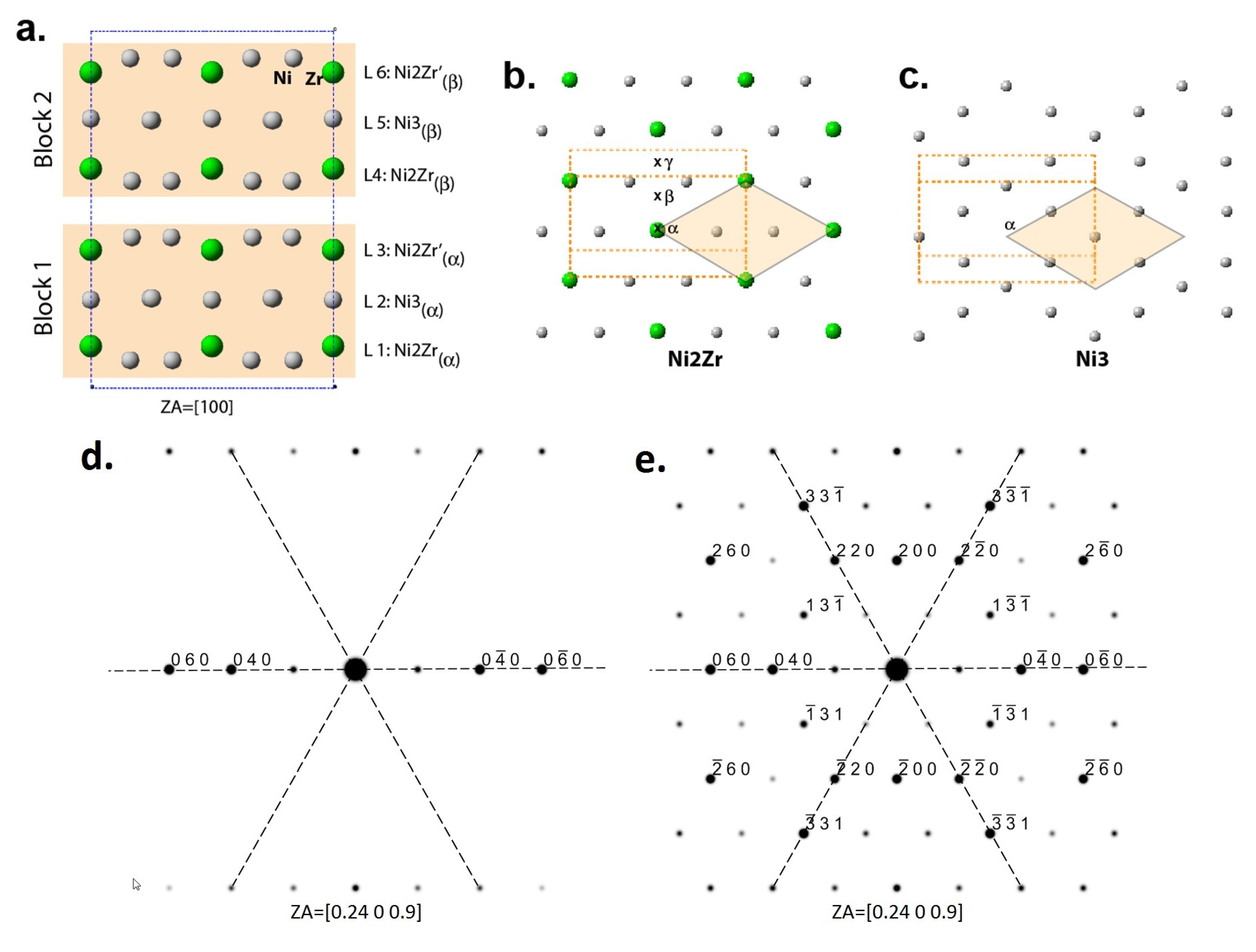
3.3. Software Simulation of Zr2Ni7 Fine Crystallites

From the TEM study of the fine structure of the Zr2Ni7 phase, it is concluded that the crystallite size of this phase is very small. According to the XRD profile of Zr2Ni7, it is rather complicated due to its monoclinic nature unlike what is seen in the experimental XRD pattern. However, it is possible for several peaks to overlap as the crystallite size becomes smaller. In order to estimate the crystallite size of Zr2Ni7, a series of simulated XRD patterns for Zr2Ni7 with various crystallite sizes under the assumption of 50% Gaussian and 50% Lorentzian distributions are built and shown in Figure 9. As the crystallite size reduces, the XRD peaks become broader and start to overlap. When the crystallite size is below 5 nm, two board peaks centered at around 38.1° and 44.3° are observed. We therefore conclude that those two broad peaks observed in the XRD pattern of the Zr8Ni21 alloy are from the nano-sized Zr2Ni7 phase formed by planar defects.
Figure 9. Simulated XRD profile assuming 50% Gaussian and 50% Lorentzian distribution of un-strained crystallite size of 1000 (a); 500 (b); 100 (c); and 50 Å (d). The reflections from the Zr2Ni7 phase are labeled at the bottom. Peak positions and intensities are from PDF 00-026-1291.
Materials 08 04618 g009

4. Conclusions

The microstructure of an annealed alloy of Zr8Ni21 composition consists of three phases, Zr8Ni21, Zr2Ni7, and Zr7Ni10. Annealing at 960 °C, which was intended to convert a cast structure into a single-phase Zr8Ni21 structure, was clearly insufficient. Distribution of the phases and their morphology can be understood with the help of a Zr-Ni phase diagram and is formed by several reactions in the following sequence: (1) L → Zr2Ni7 + L’; (2) peritectic Zr2Ni7 + L’ → Zr2Ni7 + Zr8Ni21 + L”; (3) eutectic L” → Zr8Ni21 + Zr7Ni10. TEM and crystallographic analysis of the Zr2Ni7 phase show a high density of planar (001) defects, which were explained as low-energy boundaries between 60° rotational variants and stacking faults of near-hexagonal (001) planes. The crystallographic features can be understood as arising from the pseudo-hexagonal nature of Zr2Ni7, which can be seen as a stacking of near-hexagonal layers with the following sequence: Ni2Zr(α)-Ni3(α)-Ni2Zr’(α)-Ni2Zr(β)-Ni3(β)-Ni2Zr’(β). This highly defective structure of Zr2Ni7 contributes to those two broad peaks observed in XRD analysis.

Acknowledgments

This work is financially supported by ARPA-E under the robust affordable next generation EV-storage (RANGE) program (DE-AR0000386).

Author Contributions

Kwo Young and Jean Nei prepared the ingot sample. Kwo Young and Jean Nei also performed the ICP and XRD measurement. Haoting Shen collected the EDS data and prepared the sample for TEM. Leonid A. Bendersky and Haoting Shen performed the TEM observation and discussed the results. All the authors made significant contributions to the writing of this manuscript.

Conflicts of Interest

The authors declare no conflict of interest.

References

  1. Fetcenko, M.A.; Ovshinsky, S.R.; Young, K.; Reichman, B.; Fierro, C.; Koch, J.; Martin, F.; Mays, W.; Ouchi, T.; Sommers, B.; Zallen, A. High catalytic activity disordered VTiZrNiCrCoMnAlSn hydrogen storage alloys for nickel-metal hydride batteries. J. Alloys Compd. 2002, 330–332, 752–759. [Google Scholar] [CrossRef]
  2. Young, K.; Ouchi, T.; Koch, J.; Fetcenko, M.A. The role of Mn in C14 Laves phase multi-component alloys for NiMH battery application. J. Alloys Compd. 2009, 477, 749–758. [Google Scholar] [CrossRef]
  3. Young, K.; Wong, D.F.; Yasuoka, S.; Ishida, J.; Nei, J.; Koch, J. Different failure modes for V-containing and V-free AB2 metal hydride alloys. J. Power Sources 2014, 251, 170–177. [Google Scholar] [CrossRef]
  4. Ovshinsky, S.R.; Fetcenko, M.A. A nickel metal hdride battery for electric vehicles. J. Ross. Science 1993, 260, 176–181. [Google Scholar]
  5. Young, K.; Fetcenko, M.A.; Koch, J.; Morii, K.; Shimizu, T. Studies of Sn, Co, Al, and Fe additives in C14/C15 Laves alloys for NiMH battery application by orthogonal arrays. J. Alloys Compd. 2009, 486, 559–569. [Google Scholar] [CrossRef]
  6. Young, K.; Ouchi, T.; Yang, J.; Fetcenko, M.A. Studies of off-stoichiometric AB2 metal hydride alloy: Part 1. Structural characteristics. Int. J. Hydrogen Energy 2011, 36, 11137–11145. [Google Scholar] [CrossRef]
  7. Young, K.; Nei, J. The current status of hydrogen storage alloy development for electrochemical applications. Materials 2013, 6, 4574–4608. [Google Scholar] [CrossRef]
  8. Young, K.; Young, M.; Chang, S.; Huang, B. Synergetic effects in electrochemical properties of ZrVxNi4.5−x (x = 0.0, 0.1, 0.2, 0.3, 0.4 and 0.5) metal hydride alloys. J. Alloys Compd. 2013, 560, 33–41. [Google Scholar] [CrossRef]
  9. Young, M.; Chang, S.; Young, K.; Nei, J. Hydrogen storage properties of ZrVxNi3.5−x (x = 0.0–0.9) metal hydride alloys. J. Alloys Compd. 2013, 580, S171–S174. [Google Scholar] [CrossRef]
  10. Wright, R.B.; Jolley, J.G.; Owens, M.; Cocke, D.L. Catalytic hydrogenation activity of a ZrNi3 intermetallic alloy. J. Vac. Sci. Technol. 1987, A5, 586–589. [Google Scholar] [CrossRef]
  11. Nei, J.; Young, K.; Salley, S.O.; Ng, K.Y.S. Effects of annealing on Zr8Ni19X2 (X = Ni, Mg, Al, Sc, V, Mn, Co, Sn, La and Hf): Structural characteristics. J. Alloys Compd. 2012, 516, 144–152. [Google Scholar] [CrossRef]
  12. Nei, J.; Young, K.; Salley, S.O.; Ng, K.Y.S. Effects of annealing on Zr8Ni19X2 (X = Ni, Mg, Al, Sc, V, Mn, Co, Sn, La, and Hf): Hydrogen storage and electrochemical properties. Int. J. Hydrog. Energy 2012, 37, 8418–8427. [Google Scholar] [CrossRef]
  13. Yu, J.Y.; Lei, Y.Q.; Chen, C.P.; Wu, J.; Wang, Q.D. The electrochemical properties of hydrogen storage Zr-based Laves phase alloys. J. Alloys Compd. 1995, 231, 578–581. [Google Scholar] [CrossRef]
  14. Züttel, A.; Chartouni, D.; Nützenadel, C.; Gross, K.; Schlapbach, L. Bulk and surface properties of crystalline and amorphous Zr36(V0.33Ni0.66)64 alloy as active electrode material. J. Alloys Compd. 1998, 266, 321–326. [Google Scholar] [CrossRef]
  15. Young, K.; Ouchi, T.; Liu, B. Strucural and electrochemical properties of TixZr7-xNi10. J. Alloys Compd. 2009, 480, 521–528. [Google Scholar] [CrossRef]
  16. Young, K.; Ouchi, T.; Huang, B.; Nei, J.; Fetcenko, M.A. Studies of Ti1.5Zr5.5V0.5(MxNi1−x)9.5 (M = Cr, Mn, Fe, Co, Cu, Al): Part 2. Hydrogen storage and electrochemical properties. J. Alloys Compd. 2010, 501, 245–254. [Google Scholar] [CrossRef]
  17. Young, K.; Ouchi, T.; Huang, B.; Nei, J.; Fetcenko, M.A. Studies of Ti1.5Zr5.5V0.5(MxNi1−x)9.5 (M = Cr, Mn, Fe, Co, Cu, Al): Part 1. Structural characteristics. J. Alloys Compd. 2010, 501, 236–244. [Google Scholar] [CrossRef]
  18. Ruiz, F.C.; Castro, E.B.; Real, S.G.; Peretti, H.A.; Visintin, A.; Triaca, W.E. Electrochemical characterization of AB2 alloys used for negative electrodes in Ni/MH batteries. Int. J. Hydrogen Energy 2008, 33, 3576–3580. [Google Scholar] [CrossRef]
  19. Prina, M.; Bowman, R.C., Jr.; Kulleck, J.G. Degradation study of ZrNiH1.5 for use as actuators in gas gap heat switches. J. Alloys Compd. 2004, 373, 104–114. [Google Scholar] [CrossRef]
  20. Nei, J.; Young, K.; Regmi, R.; Lawes, G.; Salley, S.O.; Ng, K.Y.S. Gaseous phase hydrogen storage and electrochemical properties of Zr8Ni21, Zr7Ni10, Zr9Ni11 and ZrNi metal hydride alloys. Int. J. Hydrogen Energy 2012, 37, 16042–16055. [Google Scholar] [CrossRef]
  21. Escobar, D.; Srinivasan, S.; Goswami, Y.; Stefanakos, E. Hydrogen storage behavior of ZrNi 70/30 and ZrNi 30/70 composites. J. Alloys Compd. 2008, 458, 223–230. [Google Scholar] [CrossRef]
  22. Ruiz, F.C.; Castro, E.B.; Peretti, H.A.; Visintin, A. Study of the different ZrxNiy phases of Zr-based AB2 materials. Int. J. Hydrogen Energy 2010, 35, 9879–9887. [Google Scholar] [CrossRef]
  23. Powder Diffraction File (PDF) database; MSDS No. 04-002-9932; International Centre for Diffraction Data: Newtown Square, PA, USA, 2011.
  24. Jungbauer, M.; Hühn, S.; Egoavil, R.; Tan, H.; Verbeeck, J.; Van Tendeloo, G.; Moshnyaga, V. Atomic layer epitaxy of ruddlesden-popper SrO(SrTiO3)n films by means of metalorganic aerosol deposition. Appl. Phys. Lett. 2014, 105, 251603. [Google Scholar] [CrossRef]
  25. Burriel, M.; Casas-Cabanas, M.; Zapata, J.; Tan, H.; Verbeeck, J.; Solis, C.; Roqueta, J.; Skinner, S.J.; Kilner, J.A.; Van Tendeloo, G.; Santiso, J. Influence of the microstructure on the high-temperature transport properties of GdBaCo2O5.5+δ epitaxial films. Chem. Mater. 2010, 22, 5512–5520. [Google Scholar] [CrossRef]
  26. Tan, H.; Turner, S.; Yücelen, E.; Verbeeck, J.; Van Tendeloo, G. 2D atomic mapping of oxidation states in transition metal oxides by scanning transmission electron microscopy and electron energy-loss spectroscopy. Phys. Rev. Lett. 2011, 107, 107602. [Google Scholar] [CrossRef] [PubMed]
  27. D’Hondt, H.; Hadermann, J.; Abakumov, A.M.; Kalyuzhnaya, A.S.; Rozova, M.G.; Tsirlin, A.A.; Nath, R.; Tan, H.; Verbeeck, J.; Antipov, E.V.; et al. Synthesis, crystal structure and magnetic properties of the Sr2Al0.78Mn1.22O5.2 anion-deficient layered perovskite. J. Solid State Chem. 2009, 182, 356–363. [Google Scholar] [CrossRef]
  28. Chen, L.; Li, X.; Tian, G.; Li, Y.; Tan, H.; Van Tendeloo, G.; Zhu, G.; Qiu, S.; Yang, X.; Su, B. Multimodal zeolite-beta-based catalysts with a hierarchical, three-level pore structure. ChemSusChem 2011, 4, 1452–1456. [Google Scholar] [CrossRef] [PubMed]
  29. Tan, H.; Egoavil, R.; Béché, A.; Martinez, G.T.; Van Aert, S.; Verbeeck, J.; Van Tendeloo, G.; Rotella, H.; Boullay, P.; Pautrat, A.; et al. Mapping electronic reconstruction at the metal-insulator interface in LaVO3/SrVO3 heterostructures. Phys. Rev. B 2013, 88, 155123. [Google Scholar] [CrossRef]
  30. Eshelman, F.R.; Smith, J.F. The structure of Zr2Ni7. Acta Cryst. 1972, B28, 1594–1600. [Google Scholar] [CrossRef]
  31. Bsenko, L. The HfNi and ZrNi systems in the region 65–80 at.% Ni. L. J. Less Comm. Met. 1979, 63, 171–179. [Google Scholar] [CrossRef]
  32. Joubert, J.M.; Cerný, R.; Yvon, K.; Latroche, M.; Percheron-Guégan, A. Zirconium-Nickel, Zr7Ni10: Space group revision for the stoichiometric phase. Acta Cryst. 1997, C53, 1536–1538. [Google Scholar] [CrossRef]
  33. Parthé, E.; Lemaire, R. Structure block stacking in intermetallic compounds. I. The rhombohedral-hexagonal Mn+1X5n-1 and the monoclinic-hexagonal-trigonal-orthorhombic Mn+1X5n+2 structure series. Acta Cryst. 1975, B31, 1879–1889. [Google Scholar] [CrossRef]

