Article

Electrical Properties and Interfacial Studies of HfxTi1–xO2 High Permittivity Gate Insulators Deposited on Germanium Substrates

1
Department of Electrical Engineering and Electronics, University of Liverpool, Liverpool L69 3GJ, UK
2
Center for Materials and Structures, School of Engineering, University of Liverpool, Liverpool L69 3GH, UK
3
Department of Physics, University of Liverpool, Liverpool L69 7ZE, UK
4
Nano and Advanced Materials Institute, Hong Kong University of Science and Technology, Kowloon 999077, Hong Kong, China
5
Department of Electrical and Electronic Engineering, Xi’an Jiaotong-Liverpool University, Suzhou 215123, China
6
Department of Chemistry, Xi’an Jiaotong-Liverpool University, Suzhou 215123, China
*
Author to whom correspondence should be addressed.
Materials 2015, 8(12), 8169-8182; https://doi.org/10.3390/ma8125454
Submission received: 24 September 2015 / Revised: 17 November 2015 / Accepted: 24 November 2015 / Published: 2 December 2015
(This article belongs to the Special Issue Atomic Layer Deposition of Functional Materials)

Abstract

:
In this research, the hafnium titanate oxide thin films, TixHf1–xO2, with titanium contents of x = 0, 0.25, 0.9, and 1 were deposited on germanium substrates by atomic layer deposition (ALD) at 300 °C. The approximate deposition rates of 0.2 Å and 0.17 Å per cycle were obtained for titanium oxide and hafnium oxide, respectively. X-ray Photoelectron Spectroscopy (XPS) indicates the formation of GeOx and germanate at the interface. X-ray diffraction (XRD) indicates that all the thin films remain amorphous for this deposition condition. The surface roughness was analyzed using an atomic force microscope (AFM) for each sample. The electrical characterization shows very low hysteresis between ramp up and ramp down of the Capacitance-Voltage (CV) and the curves are indicative of low trap densities. A relatively large leakage current is observed and the lowest leakage current among the four samples is about 1 mA/cm2 at a bias of 0.5 V for a Ti0.9Hf0.1O2 sample. The large leakage current is partially attributed to the deterioration of the interface between Ge and TixHf1–xO2 caused by the oxidation source from HfO2. Consideration of the energy band diagrams for the different materials systems also provides a possible explanation for the observed leakage current behavior.

Graphical Abstract

1. Introduction

Recently, germanium has emerged as a promising candidate for a channel material to be used in high-speed metal-oxide-semiconductor (MOS) devices, mainly due to germanium’s high carrier mobility (approximately ×2 for electrons and ×4 for holes compared with those of silicon) [1,2,3,4,5]. However, due to the lack of stable native oxide of germanium, it was difficult to fabricate a Ge Metal-Oxide-Semiconductor Field Effect Transistor (MOSFET) and a variety of dielectric materials were attempted. Among the various candidates, hafnium-based gate stacks, such as HfO2, HfON, and LaHfOx, have proven to be possible solutions for Ge MOS devices and transistors due to their relatively good reliability and high performance [6,7,8,9]. However, the reported dielectric constants of hafnium-based gate stacks varied from 11.5 to 21, which limited further scaling into the sub-nanometer regime [10,11]. In order to overcome this problem, a number of trials were carried out to further increase the permittivity of the dielectrics. One approach was to add a smaller amount of rare earth materials to the oxides to stabilize the crystal phase with a higher relative dielectric constant, such as lanthanum doped zirconium oxide [12,13]. Similar trials were performed on the hafnium oxide deposited on the silicon substrates, although the increase in the dielectric constant was not significant [14,15]. Another possible solution was to mix hafnium oxide with other dielectric materials with higher permittivity, such as titanium oxide (with k ~ 50–80). The high dielectric constant of the titanium oxide originates from the soft phonons of titanium, and an increase in the overall dielectric constant of gate oxides after mixing HfO2 and TiO2 was achieved [16,17]. Although the addition of TiO2 improved the dielectric constant of an HfO2-based material, the small energy band gap of TiO2 [18], which would result in a large leakage current, remained an issue to be considered [17]. Thus, the influence of different amounts of titanium oxide on the properties of the HfO2-based material is of great interest. In addition, the deterioration of the interface due to the oxidation source borne by the high-κ materials was observed, and the effective passivation of the germanium surface is still an open question [3]. In order to minimize the deterioration of the interface and suppress the growth of the unstable native oxide of germanium, a number of methods have been conceived to passivate the germanium surface, such as NH3 and sulfur treatment [19,20], or inserting an interfacial layer, such as aluminum oxide [21] between the high-κ thin film and the germanium substrate.
In this work, a 0.3 nm Al2O3 interfacial layer was deposited on the germanium substrate by atomic layer deposition (ALD) to passivate the surface. Subsequently, the thin films with different content levels of the TiO2 in HfO2 were deposited by ALD. The effect of TiO2 content in hafnium oxide was explored in terms of physical and electrical properties. Furthermore, the interface quality and chemical structure between the oxides and substrates were investigated. The results of the measurements and the performance of the thin films of TiO2-HfO2 deposited on Ge substrate are presented and discussed in this paper.

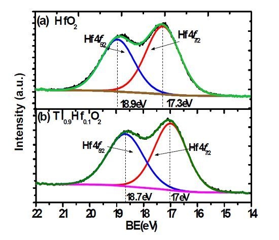
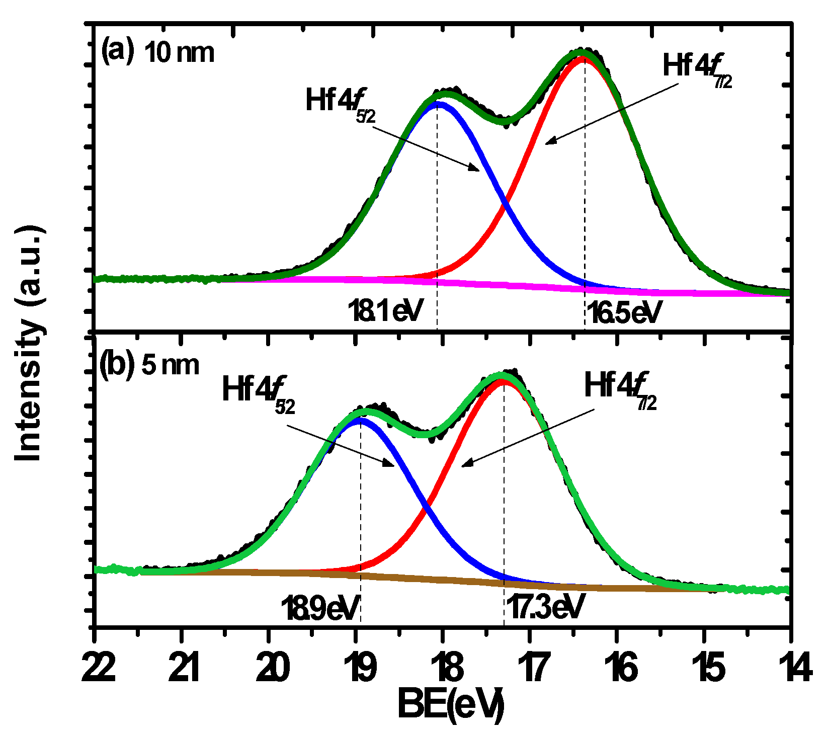
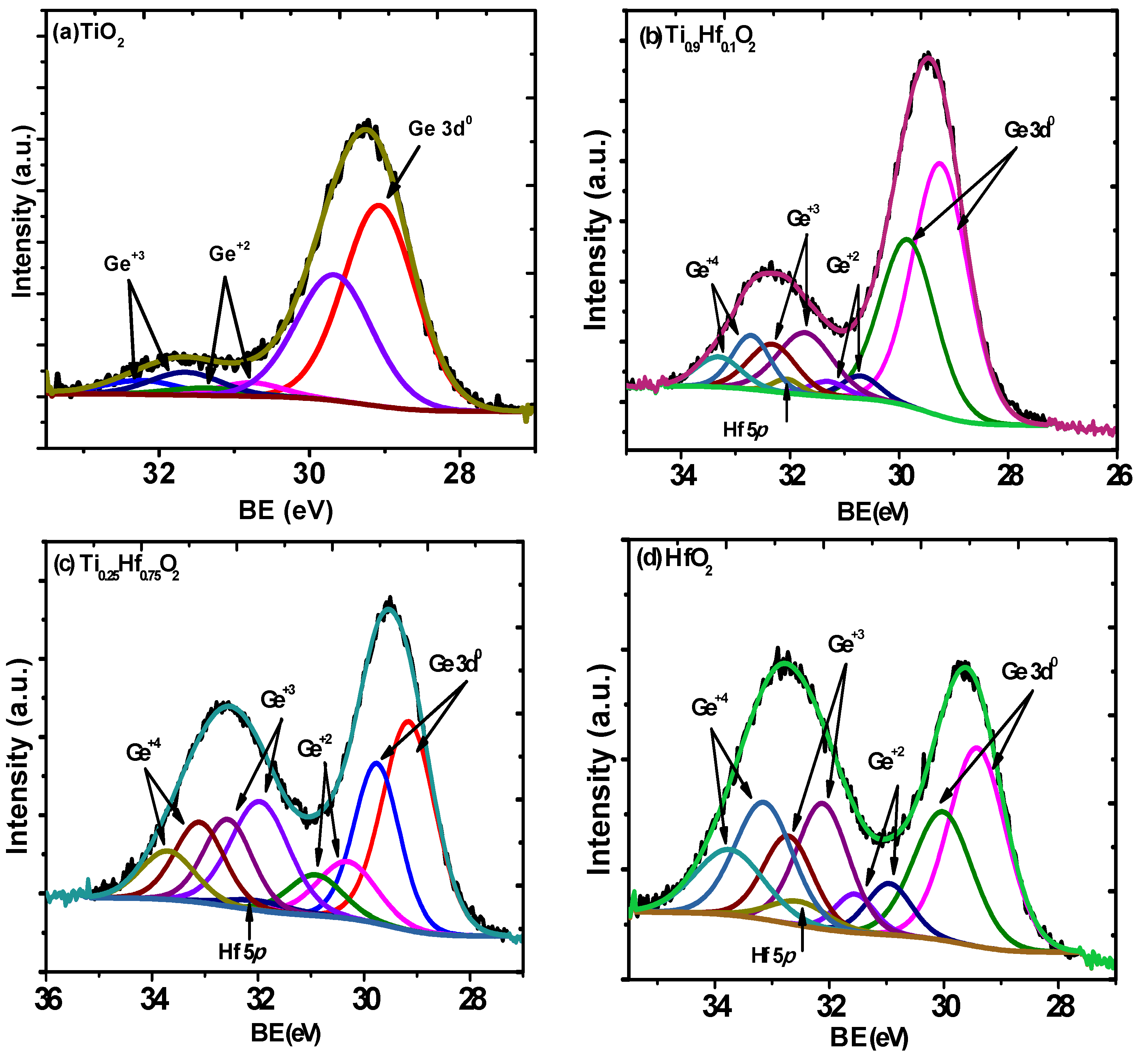
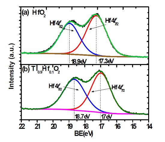
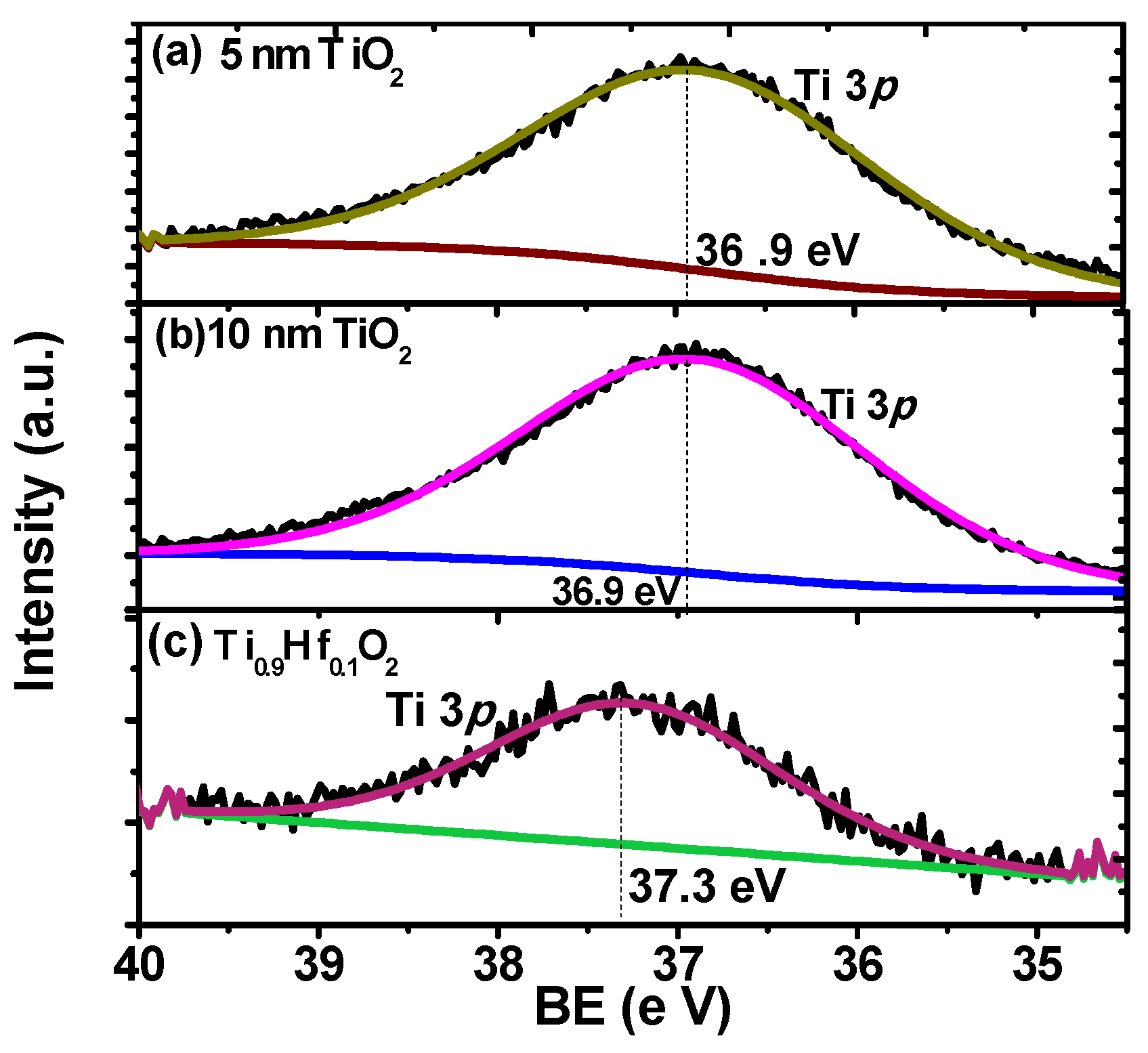
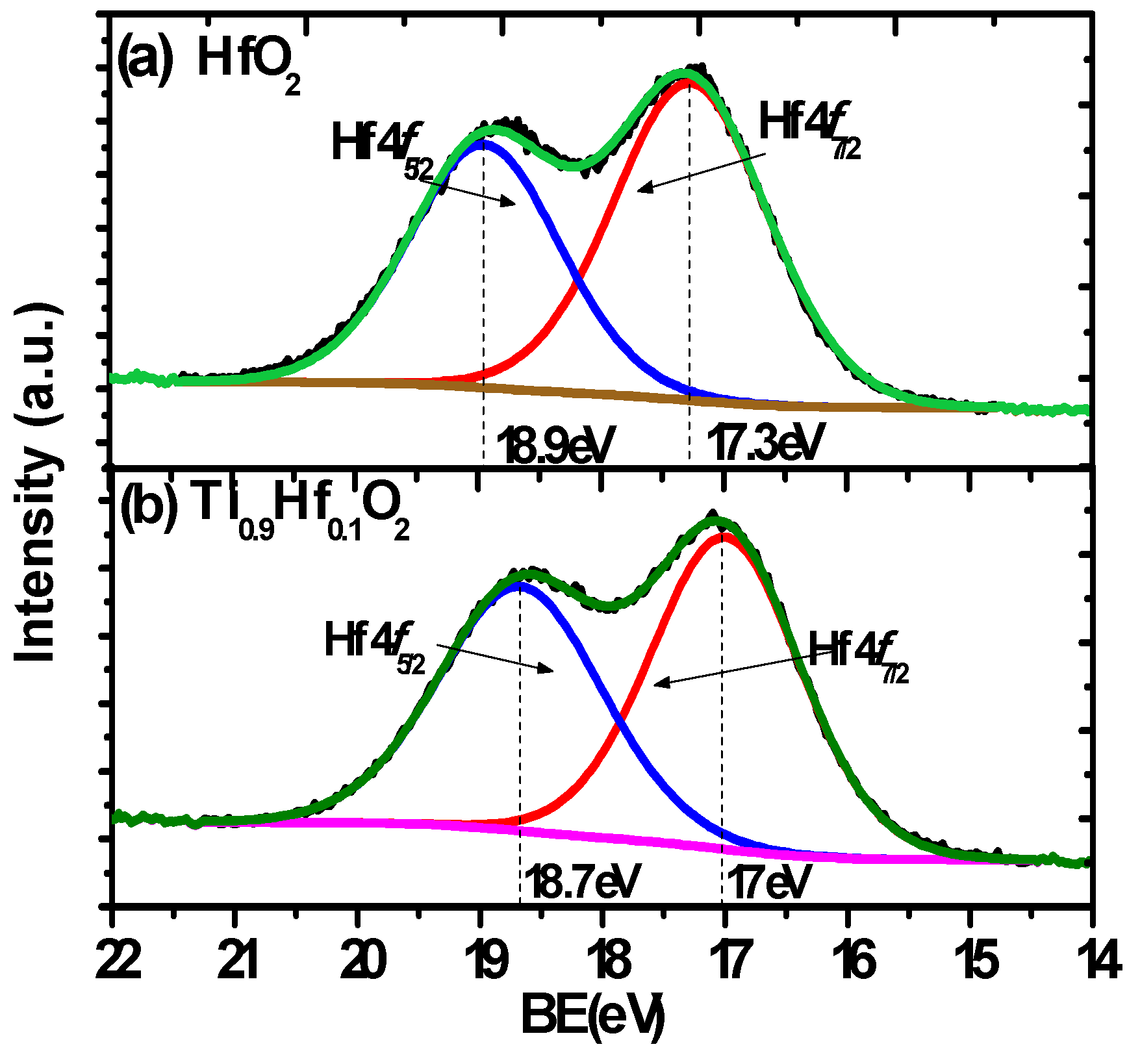
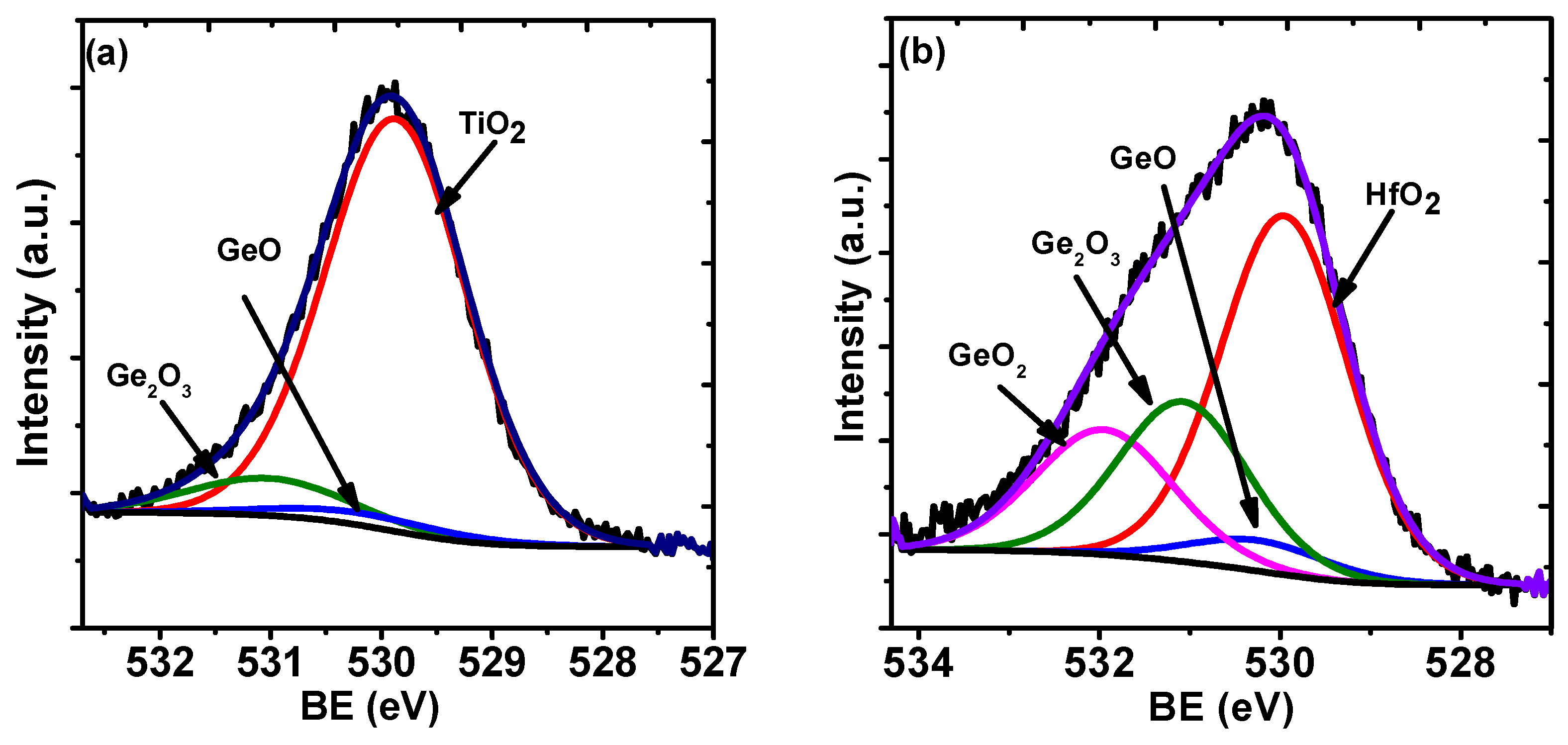
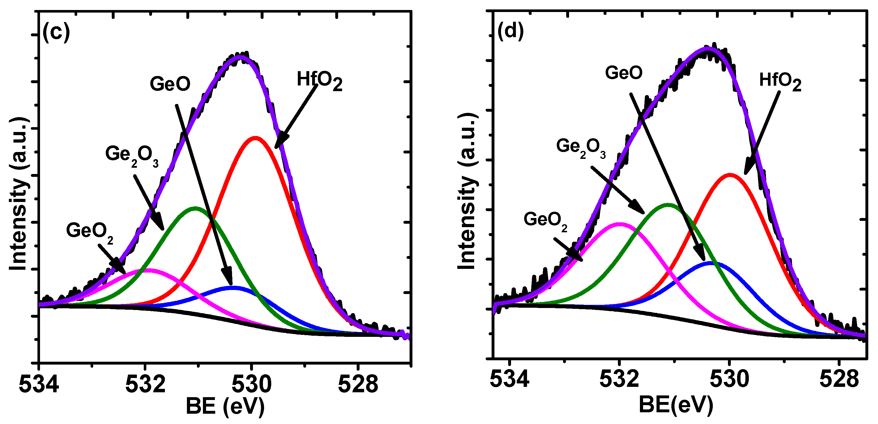
2. Results and Discussion

X-ray Photoelectron Spectroscopy (XPS) was used to characterize the quality of the interface and the thin films in the stacks. Firstly, the XPS was performed on the 5 nm and 10 nm HfO2 thin films to find out the chemical structure of the HfO2 samples in the depth direction. XPS is a surface sensitive technique so the interface was probed by using a 5 nm nominal thickness film on the germanium substrate. As shown in Figure 1a,b, the Hf 4f line shape is typically composed of a 4f5/2 and 4f7/2 spin-orbit doublet [22]. With respect to the Hf 4f7/2 peak positions, there is a clear difference between the two thin films with different thicknesses. The sample with a thickness of 10 nm has the lower binding energy (BE) peak at the position of 16.5 eV, which is tentatively assigned to stoichiometric HfO2. For the sample with a thickness of 5 nm, the binding energy of the peak is centered at 17.3 eV, a difference of 0.8 eV in comparison to the 10 nm one. This shift is indicative of the greater interaction between the HfO2 and Ge, and suggests stoichiometric and chemical changes at the interface. This is in accord with previous research, which has reported that the binding energy of Hf 4f7/2 peak in HfSixOy was 1 eV higher than that from HfO2, which has a binding energy in the range of 16.5–17 eV [23,24]. Similar results have also been found for the Ge MOS device, which stated that about a 0.5 eV shift of binding energy existed for the Hf 4f7/2 peak from HfGeOx compared with that from HfO2 [25,26]. We can thus tentatively assign the shift in the Hf 4f binding energy to the formation of a germinate, HfGeOx. In contrast, the XPS results in Figure 2a,b for the TiO2 samples in this experiment show that the Ti 3p3/2 peaks for the 5 nm and 10 nm thickness samples are centered at the same position with binding energy of 36.9 eV, suggesting that no chemical structure change occurs for the TiO2 samples in depth direction. Based upon the above analysis, it is inferred that HfO2 will react with the Ge atoms at the interface without an effective passivation of the substrate. Formation of HfGeOx at the interface deteriorates the interface and possibly increases the leakage current in the stack [26].
Figure 1. The XPS line shape for HfO2 thin films with the thickness of (a) 10 nm and (b) 5 nm. The sample with a thickness of 10 nm has the lower bonded peak at the position of 16.5 eV for Hf 4f7/2 spectra. For the sample with a thickness of 5 nm, the bonded peak for Hf 4f7/2 spectra is centered at 17.3 eV, with a difference of 0.8 eV in comparison to 10 nm one. This shift is probably due to the reaction of HfO2 with the germanium for the 5 nm HfO2 sample.
Materials 08 05454 g001
Figure 2. The Ti 3p spectra from: (a) 5 nm TiO2; (b) 10 nm TiO2; and (c) 5 nm Ti0.9Hf0.1O2 thin films. The 5 nm and 10 nm thickness TiO2 samples share the same Ti 3p3/2 binding energy centered at the 36.9 eV. A small difference, 0.4 eV, is observed in binding energy of Ti 3p spectra between TiO2 at 36.9 eV and in the Ti0.9Hf0.1O2 samples at 37.3 eV.
Materials 08 05454 g002
Figure 2c compares the Ti 3p spectrum from the Ti0.9Hf0.1O2 sample with the Ti 3p from a pure TiO2 film on germanium, while Figure 3 shows the Hf 4f7/2 spectra from the same 5 nm thick Ti0.9Hf0.1O2 sample and compares it to Hf 4f7/2 from a pure HfO2 film. It is clear that the Hf 4f7/2 binding energy from Ti0.9Hf0.1O2, 17 eV, has a smaller difference in comparison to the pure HfO2 at 17.3 eV (Ti0.25Hf0.75O2 has the same Hf 4f 7/2 binding energy as Ti0.9Hf0.1O2, 17 eV, not shown here). In addition, Figure 2a,c show that there is also a difference of 0.4 eV in the binding energy of the Ti 3p spectra between TiO2 (36.9 eV) and Ti0.9Hf0.1O2 (37.3 eV). For the Ti0.25Hf0.75O2 sample, the Ti 3p spectrum was found shifted to a higher binding energy by about 0.2 eV, while Hf 4f shifted to lower binding energy by about 0.3 eV. The shift of the Hf 4f 7/2 peak in the TixHf1–xO2 samples to a lower binding energy and the Ti 3p to a higher binding energy suggests that an electron transfer from HfO2 to TiO2 takes place as a result of chemical mixing between TiO2 and HfO2.
Figure 3. The Hf 4f spectra from 5 nm thick films of (a) HfO2 and (b) Ti0.9Hf0.1O2 on Ge. The Hf 4f7/2 binding energy from Ti0.9Hf0.1O2 is 17 eV with a smaller shift compared to the HfO2 with a shift of 17.3 eV.
Materials 08 05454 g003
In addition, from the analysis of the Ge 3d spectra from the four samples with a thickness of 5 nm shown in Figure 4, more information about the Ge surface can be deduced. The corresponding O 1s spectra from the four samples are shown in Figure 5. The peaks corresponding to Ge from elemental Ge and GeOx are labeled in the figures. The presence of Ge2+, Ge3+, and Ge4+ is due to the oxidation of the germanium substrate at the interfacial region, as well as possible germinate formation. Table 1 shows the compositions extracted from the line fits, relative to the bulk substrate Ge0 peak, of the various components at the interface for the four samples. It is clear that the oxidation is much less in the samples with TiO2 (Figure 4a) compared with the other samples, while the oxidation of the substrate in the case of HfO2 is much greater (Figure 4d). The fitting of the spectra shows an absence of Ge+4 in the TiO2 sample, while an incremental increase of the GeOx intensity, especially Ge+4, is observed with the increasing HfO2 content. This suggests that increasing the amount of HfO2 in the dielectric films provides more oxidation sources to the interface [27]. This has also been observed in other research, which states that Ge atoms were oxidized by the oxygen atoms provided by the HfO2 layer [3]. Furthermore, the Hf 4f7/2 binding energy difference for the HfO2 samples with different thickness, shown in Figure 1a,b and discussed above, also supports this finding. Therefore, it is inferred that the HfO2 is a factor in the oxidation and has a deteriorating effect on the interface. With regard to the significant binding energy shift of the Ge 3d spectra from the samples, it is partially attributed to the presence of a mixture of oxides of GeOx (where x < 2) and GeO2 at the interfacial region. The GeOx, referred to as a suboxide in the following discussion, consists of a structure with less than four oxygen atoms attached to one Ge. GeO is known to exhibit a signal at a binding energy lower than that of GeO2 [28]. In this experiment, the concentration of GeO2 and the x value differ from each other for the four samples. For Ge4+, it is absent in the pure TiO2 layer on the germanium, and it is minimal for the Ti0.9Hf0.1O2, while it is at a maximum for the pure HfO2 layer. Therefore, this behavior causes the resultant intensity of the spectral component due to GeO2 increasing, with a concomitant decrease in intensity of the peak of GeOx for oxygen rich samples, and this intensity variation leads to a shift of the overall peak [28,29]. A similar phenomenon of Ge 3d spectra shift was also observed by Caymax in the interface study of the HfO2 gate dielectric deposited on Ge [30]. In addition, the formation of HfGeOx due to the reaction between HfO2 and Ge is also a possible contributing factor to the shift of the Ge 3d spectra [25,31].
Figure 4. Ge 3d spectra from 5 nm thin films of: (a) TiO2; (b) Ti0.9Hf0.1O2; (c) Ti0.25Hf0.75O2; and (d) HfO2 samples. The presence of Ge+2, Ge+3, and Ge+4 is due to the Ge oxidation at the interfacial region. There is an increment of GeOx peak intensity, especially for Ge+4 peaks, with the increase of the HfO2 concentration.
Materials 08 05454 g004
Figure 5. O 1s spectra from 5 nm films of: (a) TiO2; (b) Ti0.9Hf0.1O2; (c) Ti0.25Hf0.75O2; and (d) HfO2.
Materials 08 05454 g005aMaterials 08 05454 g005b
Table 1. Compositions extracted from the line fits shown in Figure 4, relative to the bulk substrate Ge0 peak for the four samples.
MaterialsGe+2Ge+3Ge+4
TiO20.060.12
Ti0.9Hf 0.1O20.060.240.14
Ti0.25Hf0.75O20.170.240.41
HfO20.130.450.75
An atomic force microscope (AFM) was used to examine the surface roughness of the samples and the results for a scan area of 100 nm × 100 nm are presented in Figure 6. The surface roughness of the samples is quantitatively determined by the root-mean-squared roughness (Rrms), defined as
R rms = n = 1 N ( z n z ¯ ) 2 N 1
where zn is the measured height, z ¯ is the average height of the sample, and N is the number of measurements.
Figure 6. Atomic force microscope (AFM) images of the samples: (a) TiO2; (b) Ti0.9Hf0.1O2; (c) Ti0.25Hf0.75O2; and (d) HfO2. The roughness (Rrms) for each sample is 0.325 nm, 0.431 nm, 0.425 nm, and 0.202 nm.
Materials 08 05454 g006aMaterials 08 05454 g006b
As can be seen, all the samples exhibit good surface morphology with a roughness Rrms of 0.325 nm, 0.431 nm, 0.425 nm, and 0.202 nm for TiO2, Ti0.9Hf0.1O2, Ti0.25Hf0.75O2, and HfO2 respectively. The roughness of the thin films less than 0.5 nm demonstrates a nearly atomically smooth surface [32].
Figure 7 shows the XRD patterns for the four samples with different compositions of TiO2 and HfO2. The measurement was performed on the samples with a nominal thickness of 10 nm (the actual thickness was in the range 8 to 11 nm determined by ellipsometer). For all the samples, no noticeable diffraction peaks are observed, except for the one coming from the substrate centered at around 31.5°. According to the results of the XRD patterns only, it seems that all the thin films remained amorphous under these deposition conditions. However, due to the small thickness of the thin films, around 10 nm, the sensitivity of the XRD is probably not sufficient to detect a limited amount of the crystalline phase if it is present in the thin films, as has been previously pointed out [33,34]. It is possible that TEM (or SEAD) could further prove the exact morphology of the thin films.
Figure 7. XRD patterns for the 10 nm HfO2, Ti0.25Hf0.75O2, Ti0.9Hf0.1O2, and TiO2 thin films deposited on the germanium substrate. No noticeable diffraction peaks are observed, except for the one from the substrate.
Materials 08 05454 g007
The Capacitance-Voltage (CV) curves were obtained by sweeping the gate voltage from −1 V to 0.5 V in both directions (ramp up and ramp down) at a frequency of 1 MHz using an Agilent 4284A LCR meter (Agilent, Santa, CA, USA). Due to an unacceptable distortion of the CV characteristics caused by a large leakage current for the TiO2 sample, reported below, only the CV curves extracted from HfO2, Ti0.25Hf0.75O2, and Ti0.9Hf0.1O2 samples are presented in Figure 8. The high frequency CV measurements on the three as-grown thin films show that the samples have low trap densities because there is almost no hysteresis between the ramp up and ramp down of the CV curves. Due to the dielectric relaxation, likely caused by parasitic effect, lossy interfacial layer, and surface roughness of the samples, the obvious frequency dispersion of the samples is observed. Therefore, the vertical change of the CV characteristics is not discussed in this paper [35,36,37]. Regarding the CV characteristics of the Ti0.25Hf0.75O2 sample, it is noted that saturation in the accumulation region is not obtained, regardless of the bias voltage level. This behavior is attributed to the large leakage current for this sample, which is possibly partially related to the deterioration of the interface as discussed above in the section for XPS analysis. Further comments regarding the leakage current are made in the following section.
Figure 8. CV characteristics for the three samples of Ti0.9Hf0.1O2, Ti0.25Hf0.75O2, and HfO2. The gate voltage was swept from −1 V to 0.5 V at a frequency of 1 MHz, and no horizontal shift is observed. For the CV characteristics of the Ti0.25Hf0.75O2 sample, saturation in the accumulation region is not obtained regardless of the bias voltage level, which is attributed to the large leakage current observed in this sample.
Materials 08 05454 g008
Figure 9 illustrates the relationship between the gate leakage current density (Jg) and the bias voltage (Vg) of the samples. The maximum current limit on our instrument was set at 2 mA. From observations drawn from Figure 9, it is apparent that the titanium oxide has the highest leakage current level, followed by hafnium oxide and Ti0.25Hf0.75O2 thin films, both of which have similar leakage current levels. The Ti0.9Hf0.1O2 sample has the lowest leakage current, with less than 1 mA/cm2 at a bias voltage of 0.5 V. The large leakage current for the TiO2 sample is attributed to the small band gap of TiO2 as shown in Figure 10a and discussed further below. For the Ti0.9Hf0.1O2, Ti0.25Hf0.75O2, and HfO2 samples with a larger band gap, it is clear that the leakage current increases with greater amounts of HfO2. Previous research has also reported that a large leakage current was caused by the formation of HfGeOx at the interface between HfO2 and Ge, and the leakage current was reduced if a germanium nitride barrier layer was first introduced, preventing the formation of HfGeOx [3]. High leakage current behavior, therefore, is probably due to the deterioration of the interfacial layer caused by the interaction of HfO2 and Ge, which is consistent with the results shown in Figure 4. Thus, the increase in the leakage current clearly correlates with the hafnium oxide rich samples. For the TiO2 doped samples, the TiO2 would react with HfO2 to form HfTiOx, consuming the HfO2, which would otherwise have reacted with the Ge at the interface. It is also possible that other mechanisms may also exist to suppress the leakage current, as has been observed in the titanium doped tantalum oxide. Titanium doping was found to suppress the oxygen vacancies in tantalum oxide capacitors, which resulted in a significant reduction in the leakage current [38]. For the HfO2 capacitors, there are also a considerable number of oxygen vacancies [39,40,41,42], which could potentially be suppressed when titanium is doped in the HfO2.
Figure 9. Gate leakage current density (Jg) versus gate voltage (Vg) for samples of HfO2, Ti0.25Hf0.75O2, Ti0.9Hf0.1O2, and TiO2. The titanium oxide occupies the highest leakage current level followed by hafnium oxide and Ti0.25Hf0.75O2 thin films with similar leakage current levels. The Ti0.9Hf0.1O2 sample has the lowest leakage current.
Materials 08 05454 g009
Although the titanium incorporation seems to suppress the leakage current, the leakage current is still relatively large. The energy band diagram [18,19] in Figure 10 attempts to provide a possible explanation in conjunction with the XPS results discussed above. From the energy band diagram in Figure 10a, titanium oxide has a relatively small band gap (3.2 eV), and the conduction band minimum is at 4.21 eV, while the band gap and conduction band minimum for germanium are 0.66 eV and 4.13 eV, respectively. The thin aluminum oxide with the thickness of about 0.3 nm is used to passivate the germanium surface and it has almost no contribution to suppressing the leakage current. If a voltage was applied at the gate on the TiO2/Al2O3 stack, a dramatic leakage current should be induced, considering the energy band diagram in Figure 10a. For the energy band diagram of the hafnium oxide shown in Figure 10b, the band gap is wider and the conduction band minimum is higher than that of the TiO2. Thus, the HfO2 sample has a higher potential barrier across the oxide. Therefore, the leakage current of the HfO2 is five times smaller than that of the TiO2, regardless of the deterioration of the interface caused by the oxidation of the substrate. When TiO2 is doped in HfO2, the reaction of TiO2 and HfO2 should adjust the energy band diagram as shown in Figure 10c, and the leakage current should be between that of TiO2 and HfO2 from the point view of energy band diagram. However, as mentioned above, HfO2 is considered to be an oxidation source and contributes to the interface deterioration, which enhances the leakage current for the HfO2 rich samples. Fortunately, the formation of HfTiOx in TiO2 doped HfO2 reduces the reaction between the HfO2 and the germanium and suppresses the deterioration of interface, which results in the significant reduction of leakage current. Therefore, in our case, the Ti0.25Hf0.75O2 dielectric sample has almost the same leakage current as the HfO2 sample while the Ti0.9Hf0.1O2 sample with much less HfO2 has the smallest leakage current among all samples.
Figure 10. Energy band diagrams for: (a) titanium oxide; (b) hafnium oxide; and (c) titanium doped hafnium oxide. The work function of Al is represented by WF. Titanium oxide has relativly small band gap (3.2 eV) and the conduction band minimum is 4.21 eV below the vacuum level. Modest voltages applied to the gate can result in large leakage currents. The incorporation of hafnium oxide results in a significantly wider band gap and a lower conduction band minimum compared to that of TiO2. Therefore, the resulting leakage current of HfO2 is 5 times lower than that of TiO2 for the same applied gate voltage, regardless of the interfacial deterioration, as shown in Figure 9.
Materials 08 05454 g010aMaterials 08 05454 g010b

3. Experimental Section

Before mixing HfO2 with TiO2 to form TixHf1–xO2, the ALD growth rates of TiO2 and HfO2 were tested individually. Titanium isopropoxide and methoxymethyl hafnium were used as the ALD precursors and heated to 40 °C and 100 °C, respectively. Deionized water was used as an oxygen source and argon was employed as carrier gas in all the experiments. All the deposition was performed at the substrate temperature of 300 °C. The sequence for ALD deposition was precursor pulse/purge/water pulse/purge. For both precursors, the precursor pulse duration of 3 s was followed by a purge time of 6 s. Water pulse times of 0.01 s were followed by 3 s purge times. The thickness of thin films with different ALD cycles was measured by an ellipsometer. The relationship between the film thickness and corresponding ALD cycles is shown in Figure 11. From the slopes of the fitting straight line, it was found that the deposition rates for the TiO2 and the HfO2 were approximately 0.203 Å/cycle and 0.166 Å/cycle, respectively. Based on these growth rates, the cycle ratio of the titanium oxide to the hafnium oxide was evaluated to obtain the required dielectric oxides, with the ratio of TiO2 to HfO2 being 1:3 and 9:1 (Ti0.25Hf0.75O2 and Ti0.9Hf0.1O2), respectively, in terms of thickness. For example, for Ti0.25Hf0.75O2, two TiO2 cycles (0.4 Å) were followed by seven HfO2 cycles (1.2 Å). The content of TiO2 is equal to 0.4 Å/(0.4 Å + 1.2 Å) = 25%. According to the cycle ratio and deposition rates, the total cycles for each oxide were designed to produce the required thickness of the thin films. The p-type germanium wafers were used as the substrates of ALD TixHf1–xO2 thin films. The Ge wafer was cleaned ultrasonically in acetone followed by an O2 plasma treatment. The germanium oxide on the surface was removed by cyclically rinsing with deionized water (DI water) and diluted 2% HF. The clean wafers were transferred to the ALD chamber (Oxford Instruments OpAL™, Oxford, UK) immediately to deposit an Al2O3 passivation layer (~0.3 nm) by ALD using trimethylaluminum (TMA) as precursor. The TiO2, Ti0.9Hf0.1O2, Ti0.25Hf0.75O2, and HfO2 thin films were then deposited on the Al2O3 passivated germanium substrates, respectively. XPS measurements were carried out in a UHV system consisting of Al Kα X-ray (1486.6 eV) source and a PSP vacuum systems 5-channel HSA electron energy analyzer. Due to an impurity in the carbon in the samples the C 1s peak in the spectra at 284.6 eV was used to calibrate any charging effects during measurements. The experimental XPS spectra were fitted using a Gaussian-Lorentzian line shape doublet to account for the spin-orbit splitting, using the CASAXPS fitting package. Grazing Incident X-ray diffraction (GIXRD) was carried out using a Bruker diffractometer (Bruker, Karlsruhe, Germany) with a Cu radiation source (40 kV, 40 mA), spanning a 2θ range from 20° to 50° at a scan rate of 1°/s for all measurements. The surface morphology and roughness of the thin films were analyzed using an atomic force microscope (AFM) (Bruker, Karlsruhe, Germany). The thickness of each thin film was measured by an ELLIP-SR-1 ellipsometer with the incident angle of 65° and wavelength from 300 nm to 900 nm with a step of 20 nm. The electrode contacts with a diameter of 0.3 mm and thickness of 350 nm were deposited by E-beam evaporation (TEMD-600, Beijing, China). The back surfaces of the samples were deposited with aluminum to form ohmic contact. An Aglient 4284A precision LCR meter and a Keithley 487 picoammeter (Keithley, Cleveland, USA) were employed to investigate the electrical properties of the samples. All the electrical measurements were performed in the dark at room temperature with a Faraday Cage surrounding the prober station.
Figure 11. The thin film thickness versus ALD cycles for titanium oxide and hafnium oxide, respectively. The slopes of the two fitting straight lines (y = 0.0203x + 2.0008 and y = 0.0166x) represent the corresponding deposition rates, and R2 is the coefficient of determination. The deposition rates for TiO2 and HfO2 are approximately 0.203 Å/cycle and 0.166 Å/cycle, respectively.
Materials 08 05454 g011

4. Conclusions

Hafnium titanate oxide thin films, TixHf1–xO2, with a titanium content of x = 0, 0.25, 0.9, and 1 were deposited on alumina passivated germanium substrates. XPS was used to analyze the interface quality and chemical structure. The results indicated that the HfO2 deteriorates the interface quality, leading to an enhanced leakage current. The surface roughness was analyzed with an atomic force microscope, and all the samples exhibited relatively good surface morphology with the roughness RMS of 0.202 nm, 0.425 nm, 0.431 nm, and 0.325 nm for HfO2, Ti0.25Hf0.75O2, Ti0.9Hf0.1O2, and TiO2, respectively. XRD analysis shows that all the samples are amorphous under these deposition conditions. By using electrical characterization, it is found that there is almost no hysteresis between ramp up and ramp down of the CV curves, suggesting low trap densities. A relatively large leakage current is observed, with the lowest leakage current being about 1 mA/cm2 at the bias of 0.5 V for Ti0.9Hf0.1O2. The largest leakage current is attributed to the deterioration of the interface caused by the oxidation source borne by HfO2, and the small band gap of the dielectric materials.

Acknowledgments

This research was funded in part by the National Natural and Science Foundation of China under the grant No. 11375146, the Suzhou Science and Technology Bureau of China under the grant SYG201223, and the Jiangsu Provincial Science and Technology Program under the grant BK2012636.

Author Contributions

Qifeng Lu extracted the data and drafted the manuscript. Joseph W. Roberts, Qifeng Lu and Yifei Mu prepared the samples. Jingjin Wu and Qian Zhang performed the XRD and AFM. Vinod Dhanak and Mohammed Althobaiti performed XPS. Ce Zhou Zhao monitored and led the whole research project. Ivona Z. Mitrovic, Steve Taylor, Chun Zhao, Li Yang and Paul R. Chalker participated in the discussions. All of the authors read and approved the final manuscript.

Conflicts of Interest

The authors declare no conflict of interest.

References

  1. Caymax, M.; Eneman, G.; Bellenger, F.; Merckling, C.; Delabie, A.; Wang, G.; Loo, R.; Simoen, E.; Mitard, J.; de Jaeger, B. Germanium for advanced CMOS anno 2009: A SWOT analysis. In Proceedings of the International Electron Devices Meeting, Baltimore, MD, USA, 7–9 December 2009; pp. 428–431.
  2. Saraswat, K.; Chui, C.O.; Krishnamohan, T.; Kim, D.; Nayfeh, A.; Pethe, A. High performance germanium MOSFETs. Mater. Sci. Eng. B-Solid 2006, 135, 242–249. [Google Scholar] [CrossRef]
  3. Kamata, Y. High-κ /Ge MOSFETs for future nanoelectronics. Mater. Today 2008, 11, 1–2. [Google Scholar] [CrossRef]
  4. Shang, H.; Okorn-Schmidt, H.; Chan, K.K.; Copel, M.; Ott, J.A.; Kozlowski, P.M.; Steen, S.E.; Cordes, S.A.; Wong, H.-S.P.; Jones, E.C.; Haensch, W.E. High mobility p-channel germanium MOSFETs with a thin Ge oxynitride gate dielectric. In Proceedings of the International Electron Devices Meeting, San Francisco, CA, USA, 8–11 December 2002; pp. 441–444.
  5. Goley, P.S.; Hudait, M.K. Germanium based field-effect transistors: Challenges and opportunities. Materials 2014, 7, 2301–2339. [Google Scholar] [CrossRef]
  6. Wu, D.; Lindgren, A.-C.; Persson, S.; Sjoblom, G.; Haartman, M.V.; Seger, J.; Hellstrom, P.E.; Olsson, J.; Blom, H.O.; Zhang, S.L. A novel strained Si0.7Ge0.3 surface-channel pMOSFET with an ALD TiN/Al2O3/HfAlOx/Al2O3 Gate Stack. IEEE Electron Devices Lett. 2003, 24, 171–173. [Google Scholar] [CrossRef]
  7. Houssa, M.; Jaeger, B.D.; Delabie, A.; Elshocht, S.V.; Afanas’ev, V.V.; Autran, J.L.; Stesmans, A.; Meuris, M.; Heyns, M.M. Electrical characteristics of Ge/GeOx(N)/HfO2 gate stacks. J. Non-Cryst. Solids 2005, 351, 1902–1905. [Google Scholar] [CrossRef]
  8. Zhao, Y. Design of higher-k and more stable rare earth oxides as gate dielectrics for advanced CMOS devices. Materials 2012, 5, 1413–1438. [Google Scholar] [CrossRef]
  9. Wu, N.; Zhang, Q.C.; Zhu, C.X.; Chan, D.S.H.; Li, M.F.; Balasubramanian, N.; Chin, A.; Kwong, D.L. Alternative surface passivation on germanium for metal-oxide semiconductor applications with high-κ gate dielectric. Appl. Phys. Lett. 2004, 85, 4127–4129. [Google Scholar] [CrossRef]
  10. Chen, J.J.-H.; Bojarczuk, N.A.; Shang, H., Jr.; Copel, M.; Hannon, J.B.; Karasinski, J.; Preisler, E.; Banerjee, S.K.; Guha, S. Ultrathin Al2O3 and HfO2 gate dielectrics on surface-nitrided Ge. IEEE Trans. Electron Devices 2004, 51, 1441–1447. [Google Scholar] [CrossRef]
  11. Li, X.F.; Liu, X.J.; Zhang, W.Q.; Fu, Y.; Li, A.D.; Li, H.; Wu, D. Comparison of the interfacial and electrical properties of HfAlO films on Ge with S and GeO2 passivation. Appl. Phys. Lett. 2011, 98. [Google Scholar] [CrossRef]
  12. Zhao, C.Z.; Taylor, S.; Werner, M.; Chalker, P.R.; Murray, R.T.; Gaskell, J.M.; Jones, A.C. Dielectric relaxation of lanthanum doped zirconium oxide. Appl. Phys. Lett. 2009, 105. [Google Scholar] [CrossRef]
  13. Lu, Q.; Zhao, C.; Mu, Y.; Zhao, C.Z.; Taylor, S.; Chalker, P.R. Hysteresis in lanthanide zirconium oxides observed using a pulse CV technique and including the effect of high temperature annealing. Materials 2015, 8, 4829–4842. [Google Scholar] [CrossRef]
  14. Huang, L.Y.; Li, A.D.; Zhang, W.Q.; Li, H.; Xia, Y.D.; Wu, D. Fabrication and characterization of La-doped HfO2 gate dielectrics by metal-organic chemical vapor deposition. Appl. Surf. Sci. 2010, 256, 2496–2499. [Google Scholar] [CrossRef]
  15. Wang, T.; Ekerdt, J.G. Atomic layer deposition of lanthanum stabilized amorphous hafnium oxide thin films. Chem. Mater. 2009, 21, 3096–3101. [Google Scholar] [CrossRef]
  16. Chen, F.; Bin, X.; Hella, C.; Shi, X.; Gladfelter, W.L.; Campbell, S.A. A Study of mixtures of HfO2 and TiO2 as high-κ gate dielectrics. Microelectron. Eng. 2004, 72, 263–266. [Google Scholar] [CrossRef]
  17. Werner, M.; Peter, P.J.; Hindley, S.; Romani, S.; Mather, S.; Chalker, P.R.; Williams, P.A.; Van, D.B.; Jakob, A. Atomic layer deposition of Ti-HfO2 dielectrics. Appl. Phys. Lett. 2013, 31. [Google Scholar] [CrossRef]
  18. Xu, Y.; Schoonen, M.A.A. The absolute energy positions of conduction and valence bands of selected semiconducting minerals. Am. Mineral. 2000, 85, 543–556. [Google Scholar] [CrossRef]
  19. Van Elshocht, S.; Brijs, B.; Caymax, M.; Conard, T.; Chiarella, T.; de Gendt, S.; de Jaeger, B.; Kubicek, S.; Meuris, M.; Onsia, B.; et al. Deposition Of HfO2 on germanium and the impact of surface pretreatments. Appl. Phys. Lett. 2004, 85. [Google Scholar] [CrossRef]
  20. Xie, R.; Zhu, C. Effects of sulfur passivation on germanium MOS capacitors with HfON gate dielectric. IEEE Electron Devices Lett. 2007, 28, 976–979. [Google Scholar] [CrossRef]
  21. Kato, R.; Kyogoku, S.; Sakashita, M.; Kondo, H.; Zaima, S. Effects of atomic layer deposition-Al2O3 interface layers on interfacial properties of ge metal oxide semiconductor capacitors. Jpn. J. Appl. Phys. 2009, 48. [Google Scholar] [CrossRef]
  22. Sahin, D.; Yildiz, I.; Gencer, A.I.; Aygun, G.; Turan, R. Evolution of SiO2/Ge/HfO2(Ge) multilayer structure during high temperature annealing. Thin Solid Films 2010, 518, 2365–2369. [Google Scholar] [CrossRef]
  23. Cho, M.H.; Roh, Y.S.; Whang, C.N.; Jeong, K.; Nahm, S.W.; Ko, D.H.; Lee, J.H.; Lee, N.I.; Fujihara, K. Thermal stability and structural characteristics of HfO2 films on Si(100) grown by atomic-layer deposition. Appl. Phys. Lett. 2002, 81, 472–474. [Google Scholar] [CrossRef]
  24. Opila, R.L.; Wilk, G.D.; Alam, M.A.; van Dover, R.B.; Busch, B.W. Photoemission study of Zr- and Hf-silicates for use as high-κ oxides: Role of second nearest neighbors and interface charge. Appl. Phys. Lett. 2002, 81, 1788–1790. [Google Scholar] [CrossRef]
  25. Van Elshocht, S.; Caymax, M.; Conard, T.; de Gendt, S.; Hoflijk, I.; Houssa, M.; de Jaeger, B.; van Steenbergen, J.; Heyns, M.; Meuris, M. Effect of hafnium germanate formation on the interface of HfO2/germanium metal oxide semiconductor devices. Appl. Phys. Lett. 2006, 88. [Google Scholar] [CrossRef]
  26. Xie, Q.; Deng, S.; Schaekers, M.; Lin, D.; Caymax, M.; Delabie, A.; Qu, X.; Jiang, Y.; Deduytsche, D.; Detavernier, C. Germanium surface passivation and atomic layer deposition of high-κ dielectrics—A tutorial review on Ge-based MOS capacitors. Semicond. Sci. Technol. 2012, 27. [Google Scholar] [CrossRef]
  27. Curreem, K.K.S.; Lee, P.F.; Wong, K.S.; Dai, J.Y.; Zhou, M.J.; Wang, J.; Li, Q. Comparison of interfacial and electrical characteristics of HfO2 and HfAlO high-κ dielectrics on compressively strained Si1−xGex. Appl. Phys. Lett. 2006, 88. [Google Scholar] [CrossRef]
  28. Prabhakaran, K.; Maeda, F.; Watanabe, Y.; Ogino, T. Distinctly different thermal decomposition pathways of ultrathin oxide layer on Ge and Si surfaces. Appl. Phys. Lett. 2000, 76, 2244–2246. [Google Scholar] [CrossRef]
  29. Schmeisser, D.; Schnell, R.D.; Bogen, A.; Himpsel, F.J.; Rieger, D.; Landgren, G.; Morar, J.F. Surface oxidation states of germanium. Surf. Sci. 1986, 172, 455–465. [Google Scholar] [CrossRef]
  30. Caymax, M.; van Elshocht, S.; Houssa, M.; Delabie, A.; Conard, T.; Meuris, M.; Heyns, M.M.; Dimoulas, A.; Spiga, S.; Fanciulli, M.; et al. HfO2 as gate dielectric on Ge: Interfaces and deposition techniques. Mat. Sci. Eng. B-Solid 2006, 135, 256–260. [Google Scholar] [CrossRef]
  31. Kita, K.; Takahashi, T.; Nomura, H.; Suzuki, S.; Nishimura, T.; Toriumi, A. Control of high-κ /germanium interface properties through selection of high-κ materials and suppression of GeO volatilization. Appl. Surf. Sci. 2008, 254, 6100–6105. [Google Scholar] [CrossRef]
  32. Li, M.; Zhang, Z.; Campbell, S.A.; Li, H.J.; Peterson, J.J. Hafnium titanate as a high permittivity gate insulator: Electrical and physical characteristics and thermodynamic stability. J. Appl. Phys. 2007, 101. [Google Scholar] [CrossRef]
  33. Delabie, A.; Puurunen, R.L.; Brijs, B.; Caymax, M.; Conard, T.; Onsia, B.; Richard, O.; Vandervorst, W.; Zhao, C.; Heyns, M.M.; et al. Atomic layer deposition of hafnium oxide on germanium substrates. J. Appl. Phys. 2005, 97, 64104. [Google Scholar] [CrossRef]
  34. Ardalan, P.; Pickett, E.R.; Harris, J.S.; Marshall, A.F.; Bent, S.F. Formation of an oxide-free Ge/TiO2 interface by atomic layer deposition on brominated Ge. Appl. Phys. Lett. 2008, 92. [Google Scholar] [CrossRef]
  35. Tao, J.; Zhao, C.Z.; Zhao, C.; Taechakumput, P.; Werner, M.; Taylor, S.; Chalker, P.R. Extrinsic and intrinsic frequency dispersion of high-κ materials in capacitance-voltage measurements. Materials 2012, 5, 1005–1032. [Google Scholar] [CrossRef]
  36. Lee, B.; Moon, T.; Kim, T.; Choi, D.; Park, B. Dielectric relaxation of atomic-layer-deposited HfO2 thin films from 1 kHz to 5 GHz. Appl. Phys. Lett. 2005, 87. [Google Scholar] [CrossRef]
  37. Zhao, C.; Zhao, C.Z.; Werner, M.; Taylor, S.; Chalker, P. Dielectric relaxation of high-κ oxides. Nanoscale Res. Lett. 2013, 8, 1–12. [Google Scholar] [CrossRef] [PubMed]
  38. Lau, W.S.; Tan, T.S.; Babu, P.; Sandler, N.P. Mechanism of leakage current reduction of tantalum oxide capacitors by titanium doping. Appl. Phys. Lett. 2007, 90. [Google Scholar] [CrossRef]
  39. Chen, Y.Y. Electrical characteristics of the uniaxial-strained nMOSFET with a fluorinated HfO2/SiON gate stack. Materials 2014, 7, 2370–2381. [Google Scholar] [CrossRef]
  40. Ji, M.; Wang, L.; Du, J. Preparation and characterization of Gd2O3-doped HfO2 high-κ gate dielectric thin films by RF sputtering. J. Phys. Conf. Ser. 2009, 152. [Google Scholar] [CrossRef]
  41. Guha, S.; Narayanan, V. Oxygen vacancies in high dielectric constant oxide-semiconductor films. Phys. Rev. Lett. 2007, 98. [Google Scholar] [CrossRef] [PubMed]
  42. Miyata, N. Study of direct-contact HfO2/Si interfaces. Materials 2012, 5, 512–527. [Google Scholar] [CrossRef]

