Graphene as a Buffer Layer for Silicon Carbide-on-Insulator Structures

Abstract
:1. Introduction
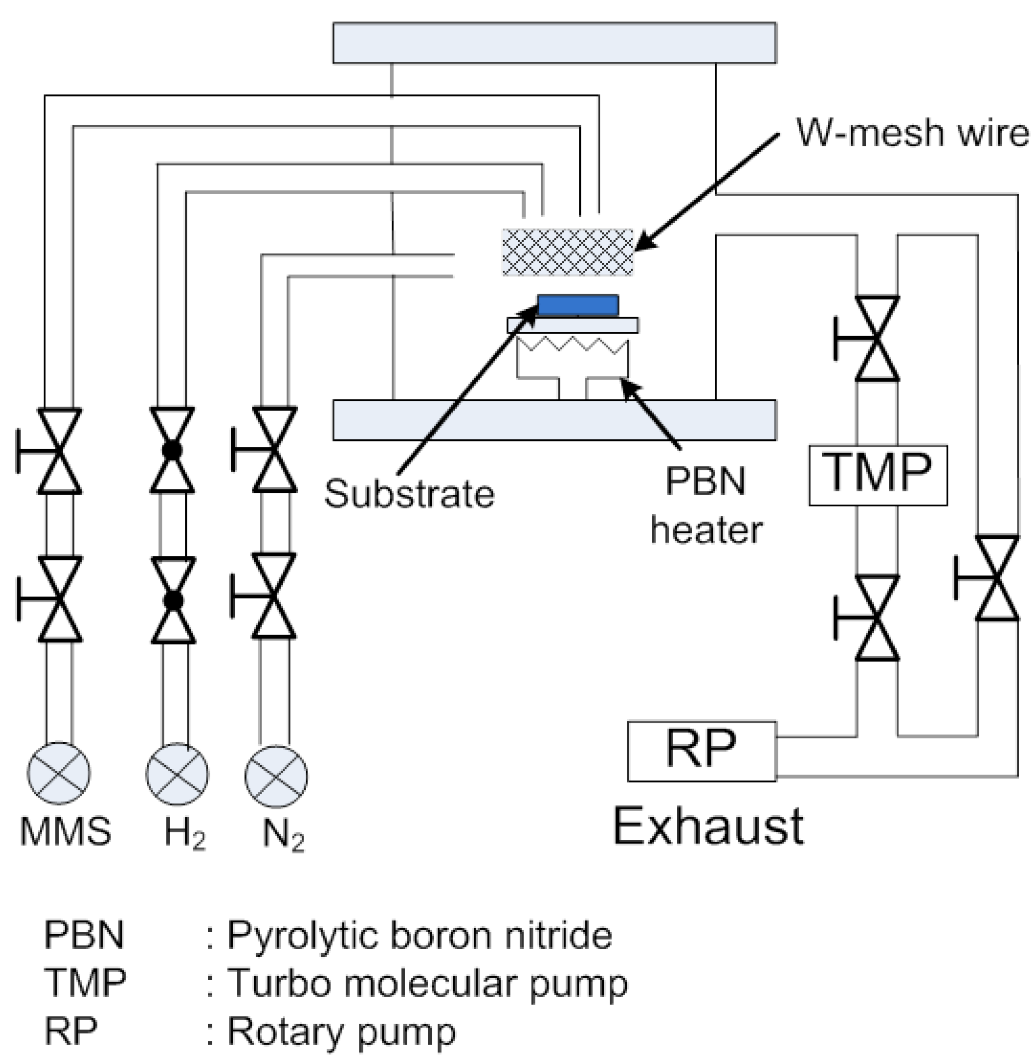
2. Experimental


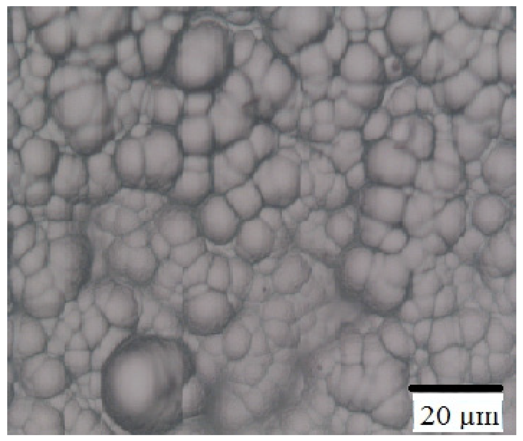
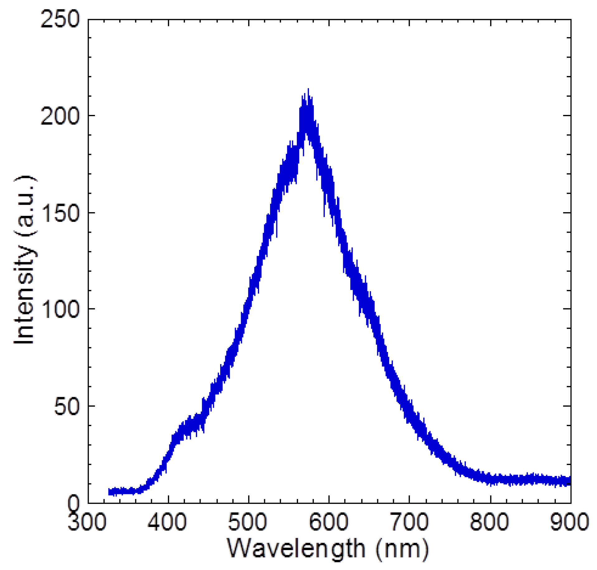
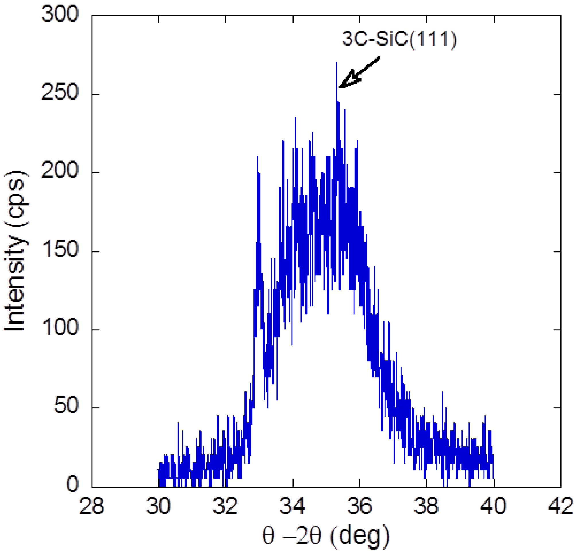
3. Results and Discussion


4. Conclusions
Acknowledgments
References
- Pillarisetty, R. Academic and industry research progress in germanium nanodevices. Nature 2011, 479, 324–328. [Google Scholar] [CrossRef] [PubMed]
- Takagi, S.; Sugiyama, M.; Yasuda, T.; Takenaka, M. Ge/III-V channel engineering for future CMOS. ECS Trans. 2009, 19, 9–20. [Google Scholar]
- Gopalakrishnan, K.; Griffin, P.B.; Ma, Kai.; Deal, M.D.; Plummer, J.D. MOSFETs and high-speed photodetectors on Ge-on-insulator substrates fabricated using rapid melt growth. In Proceeding of IEEE International Electron Devices Meeting, San Francisco, CA, USA, 13–15 December 2004.
- Itabashi, S.; Nishi, H.; Tsuchizawa, T.; Watanabe, T.; Shinojima, H.; Park, S.; Yamada, K.; Ishikawa, Y.; Wada, K. Integration of optical devices based on Si, Ge and SiOx. In Proceeding of IEEE International Conferences on Group IV Photonics (GFP), Beijing, China, 1–3 September 2010.
- Wang, J.; Lee, S. Ge photodetectors for Si-based optoelectronic integration. Sensors 2011, 11, 696–718. [Google Scholar] [CrossRef] [PubMed]
- Razykov, T.M.; Ferekides, C.S.; Morel, D.; Stefanakos, E.; Ullal, H.S.; Upadhyaya, H.M. Solar photovoltaic electricity: Current status and future prospects. Sol. Energy 2011, 85, 1580–1608. [Google Scholar] [CrossRef]
- Bolotin, K.I.; Sikes, K.J.; Jiang, Z.; Klima, M.; Fudenberg, G.; Hone, J.; Kim, P.; Stormer, H.L. Ultrahigh electron mobility in suspended graphene. Solid State Commun. 2008, 146, 351–355. [Google Scholar] [CrossRef]
- Novoselov, K.S.; Jiang, Z.; Zhang, Y.; Morozov, S.V.; Stormer, H.L.; Zeitler, U.; Maan, J.C.; Boebinger, G.S.; Kim, P.; Geim, A.K. Room temperature quantum hall effect in graphene. Science 2007, 315, 1379. [Google Scholar] [CrossRef] [PubMed] [Green Version]
- Balandin, A.A. Thermal properties of graphene and nanostructured carbon materials. Nat. Mater. 2011, 10, 569–581. [Google Scholar] [CrossRef] [PubMed]
- Balandin, A.A.; Nika, D.L. Phononics in low-dimensional materials. Mater. Today 2012, 15, 266–275. [Google Scholar] [CrossRef]
- Chen, S.; Wu, Q.; Mishra, C.; Kang, J.; Zhung, H.; Cho, K.; Cai, W.; Balandin, A.A.; Ruoff, R.S. Thermal conductivity of isotopically modified graphene. Nat. Mater. 2012, 11, 203–207. [Google Scholar] [CrossRef] [PubMed]
- Ghosh, S.; Nika, D.L.; Pokatilov, E.P.; Balandin, A.A. Heat conduction in graphene: Experimental study and theoretical interpretation. New J. Phys. 2009, 11, 095012:1–095012:19. [Google Scholar] [CrossRef]
- Chassagne, T.; Ferro, G.; Wang, H.; Stoemenos, Y.; Peyre, H.; Contreras, S.; Camassel, J.; Monteil, Y.; Ghyselen, B. Improved SiCOI structures elaborated by heteroepitaxy of 3C-SiC on SOI. Mater. Sci. Forum 2002, 389–393, 343–346. [Google Scholar] [CrossRef]
- Hashim, A.M.; Anisuzzaman, M.; Muta, S.; Sadoh, T.; Miyao, M. Epitaxial-template structure utilizing Ge-on-insulator stripe arrays with nanospacing for advanced heterogeneous integration on Si platform. Jpn. J. Appl. Phys. 2012, 51, 06FF04:1–06FF04:5. [Google Scholar] [CrossRef]
- Tsukamoto, T.; Ogino, T. Graphene-on-insulator fabricated on atomically controlled solid surfaces. J. Phys. D 2010, 43, 374014:1–374014:6. [Google Scholar]
- Bai, Y.; Cole, G.D.; Bulsara, M.T.; Fitzgerald, E.A. Fabrication of GaAs-on-insulator via low temperature wafer bonding and sacrificial etching of Ge by XeF2. J. Electrochem. Soc. 2012, 159, H183–H190. [Google Scholar] [CrossRef]
- Yasui, K.; Miura, H.; Takata, M.; Akahane, T. SiCOI structure fabricated by catalytic chemical vapor deposition. Thin Solid Films 2008, 516, 644–647. [Google Scholar] [CrossRef]
- Miura, H.; Yasui, K.; Abe, K.; Masuda, A.; Kuroki, Y.; Nishiyama, H.; Takata, M.; Inoue, Y.; Akahane, T. Epitaxial growth of SiC on silicon on insulator substrates with ultrathin top Si layer by hot-mesh chemical vapor deposition. Jpn. J. Appl. Phys. 2008, 47, 569–572. [Google Scholar] [CrossRef]
- Hashim, A.M.; Yasui, K. Carbonization layer obtained by acetylene reaction with silicon (100) and (111) surface using low pressure chemical vapor deposition. J. Appl. Sci. 2008, 9, 3473–3478. [Google Scholar] [CrossRef]
- Wu, C.H.; Zorman, C.A.; Mehregany, M. Characterization of polycrystalline SiC grown on SiO2 and Si3N4 by APCVD for MEMS application. Mater. Sci. Forum 2000, 338–342, 541–544. [Google Scholar] [CrossRef]
- Zhao, Y.M.; Sun, G.S.; Ning, J.; Liu, X.F.; Zhao, W.S.; Wang, L.; Li, J.M. Doped polycrystalline 3C-SiC films deposited by LPCVD for radio-frequency MEMS application. Chin. Phys. Lett. 2008, 25, 2269–2272. [Google Scholar] [CrossRef]
- Narita, Y.; Yasui, K.; Eto, J.; Kurimoto, T.; Akahane, T. (100)-Oriented 3C-SiC polycrystalline grown on SiO2 by hot-mesh chemical vapor deposition using monomethylsilane and hydrogen. Jpn. J. Appl. Phys. 2005, 44, L809–L811. [Google Scholar] [CrossRef]
- Ishida, M.; Ogawa, M.; Orita, K.; Imafuji, O.; Yuri, M.; Sugino, T.; Itoh, K. Drastic reduction of threading dislocation in GaN regrown on grooved stripe structure. J. Cryst. Growth 2000, 221, 345–349. [Google Scholar] [CrossRef]
- Choi, W.M.; Shin, K.S.; Lee, H.S.; Choi, D.; Kim, K.; Shin, H.J.; Yoon, S.M.; Choi, J.Y.; Kim, S.W. Selective growth of ZnO nanorods on SiO2/Si substrate using a graphene buffer layer. Nano Res. 2011, 4, 440–447. [Google Scholar] [CrossRef]
- Choi, W.; Lahiri, I.; Seelabayina, R.; Kang, Y.S. Synthesis of graphene and its application: A review. Crit. Rev. Solid State Mater. Sci. 2010, 35, 52–70. [Google Scholar] [CrossRef]
- Ferrari, A.C.; Meyer, J.C.; cardaci, V.; Casiraghi, C.; Lazzeri, M.; Mauri, F.; Piscarces, S.; Jiang, D.; Novoselov, K.S.; Roth, S.; Geim, A.K. Raman spectrum of graphene and graphene layer. Phys. Rev. Lett. 2006, 97, 187401:1–187401:4. [Google Scholar]
- Tabata, A.; Komura, Y.; Hoshida, Y.; Narita, T.; Kondo, A. Properties of nanocrystalline cubic silicon carbide thin films prepared by hot-wire chemical vapor deposition using SiH4/CH4/H2 at various substrate temperature. Jpn. J. Appl. Phys. 2008, 47, 561–565. [Google Scholar] [CrossRef]
- Ulrich, S.; Theel, T.; Schwan, J.; Batori, V.; Scheib, M.; Ehrhardt, H. Low-temperature formation of β-silicon carbide. Diam. Relat. Mater. 1997, 6, 645–648. [Google Scholar] [CrossRef]
- Yasui, K.; Eto, J.; Narita, Y.; Takata, M.; Akahane, T. Low-temperature heteroepitaxial growth of SiC on (100) Si using hot mesh chemical vapor deposition. Jpn. J. Appl. Phys. 2005, 44, 1361–1364. [Google Scholar] [CrossRef]
- Neudeck, P.G.; Larkin, D.J.; Starr, J.E.; Powell, J.A.; Salupo, C.S.; Matus, L.G. Electrical properties of epitaxial 3C- and 6H-SiC P-N junction diodes produced side by side on 6H-SiC substrates. IEEE Trans. Electron Devices 1994, 41, 826–835. [Google Scholar] [CrossRef]
- Yuan, C.; Steckl, A.J.; Chaudhuri, J.; Thokala, R.; Loboda, M.J. Reduced temperature growth of crystalline 3C-SiC films on 6H-SiC by chemical vapor deposition from silacyclobutane. J. Appl. Phys. 1995, 78, 1271–1273. [Google Scholar] [CrossRef]
- Takahashi, R.; Handa, H.; Abe, S.; Imaizumi, K.; Fukidome, H.; Yoshigoe, A.; Teraoka, Y.; Suemitsu, M. Low-energy-electron-diffraction and X-ray-photoelectron-spectroscopy studies of graphitization of 3C-SiC(111) thin film on Si(111) substrate. Jpn. J. Appl. Phys. 2011, 50, 070103:1–070103:6. [Google Scholar] [CrossRef]
- Yu, M.B.; Rusli; Yoon, S.F.; Chen, Z.M.; Ahn, J.; Zhang, Q.; Chew, K.J.; Cui, J. Deposition of nanocrystalline cubic silicon carbide films using hot-filament chemical-vapor-deposition method. J. Appl. Phys. 2000, 87, 8155–8185. [Google Scholar] [CrossRef]
- Sha, Z.D.; Wu, X.M.; Zhuge, L.J. Structure and photoluminescence properties of SiC film synthesized by RF-magnetron sputtering technique. Vacuum 2005, 79, 250–254. [Google Scholar] [CrossRef]
- Rahman, S.F.A.; Kasai, S.; Hashim, A.M. Room temperature nonlinear of a graphene-based three-branch nanojunction device with chemical doping. Appl. Phys. Lett. 2012, 100, 193116:1–193116:3. [Google Scholar]
- Liu, L.; Ryu, S.; Tomasik, M.R.; Stolyarova, E.; Jung, N.; Hybertsen, M.S.; Steigerwald, M.L.; Brus, L.E.; Flynn, G.W. Graphene oxidation: Thickness-dependent etching and strong chemical doping. Nano Lett. 2008, 8, 1965–1970. [Google Scholar] [CrossRef] [PubMed]
© 2012 by the authors. Licensee MDPI, Basel, Switzerland. This article is an open access article distributed under the terms and conditions of the Creative Commons Attribution license ( http://creativecommons.org/licenses/by/3.0/).
Share and Cite
Astuti, B.; Tanikawa, M.; Rahman, S.F.A.; Yasui, K.; Hashim, A.M. Graphene as a Buffer Layer for Silicon Carbide-on-Insulator Structures. Materials 2012, 5, 2270-2279. https://doi.org/10.3390/ma5112270
Astuti B, Tanikawa M, Rahman SFA, Yasui K, Hashim AM. Graphene as a Buffer Layer for Silicon Carbide-on-Insulator Structures. Materials. 2012; 5(11):2270-2279. https://doi.org/10.3390/ma5112270
Chicago/Turabian StyleAstuti, Budi, Masahiro Tanikawa, Shaharin Fadzli Abd Rahman, Kanji Yasui, and Abdul Manaf Hashim. 2012. "Graphene as a Buffer Layer for Silicon Carbide-on-Insulator Structures" Materials 5, no. 11: 2270-2279. https://doi.org/10.3390/ma5112270