Electronic and Optical Properties of Substitutional and Interstitial Si-Doped ZnO


Abstract
:1. Introduction
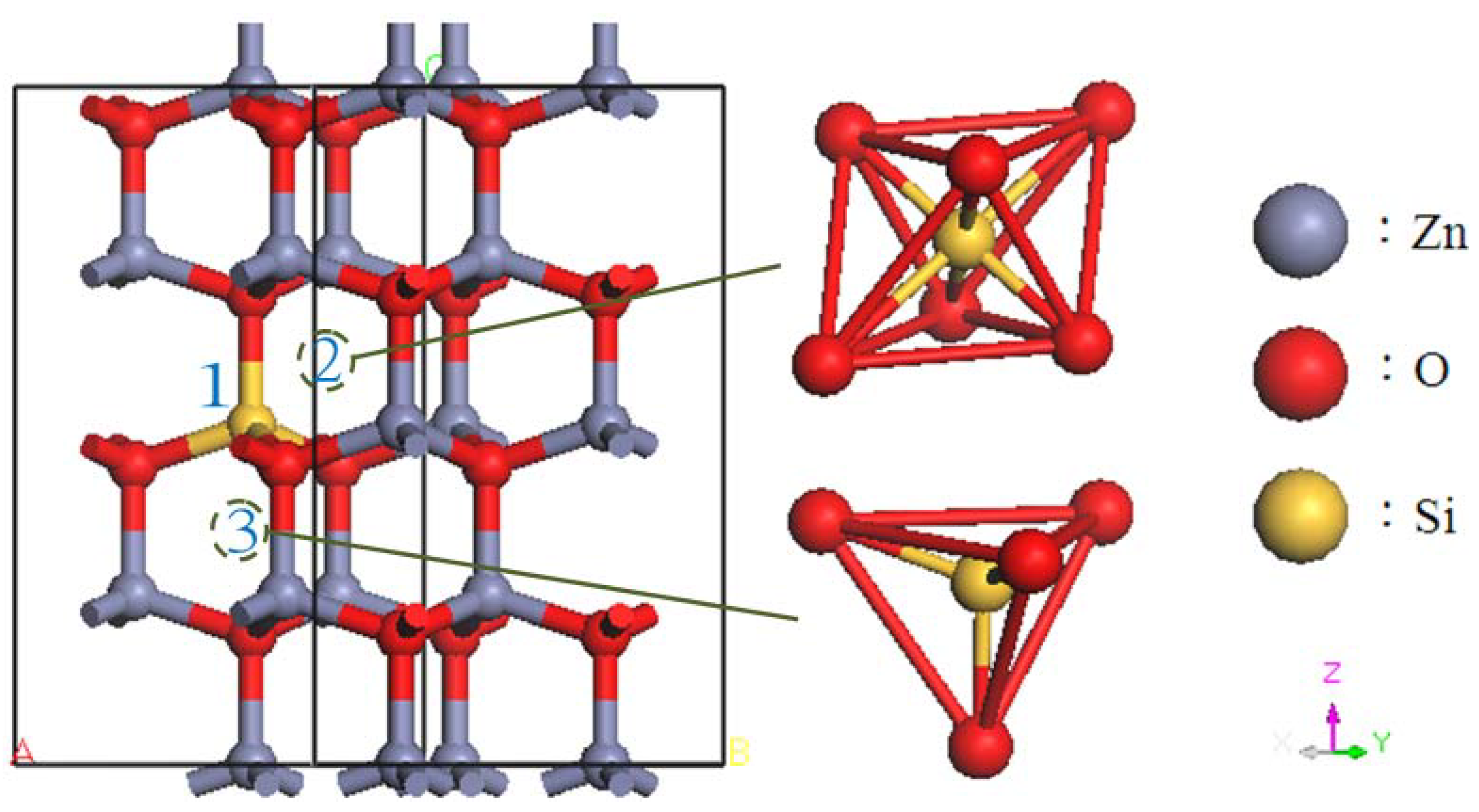
2. Calculation Models and Methods


3. Results and Discussion
3.1. Formation Energy

| Formation energy (eV) | Effective mass (m0) | Transmittance (%) | |||
|---|---|---|---|---|---|
| Zn-rich | O-rich | 200–400 nm | 400–800 nm | ||
| Pure | – | – | 0.22 | 66 | 89 |
| Sis(Zn) | 10.79 | 7.54 | 0.29 | 83 | 86 |
| Sii(oct) | 14.68 | 14.68 | 11.49 | 53 | 52 |
| Sii(tet) | 16.56 | 16.56 | 3.11 | 53 | 65 |
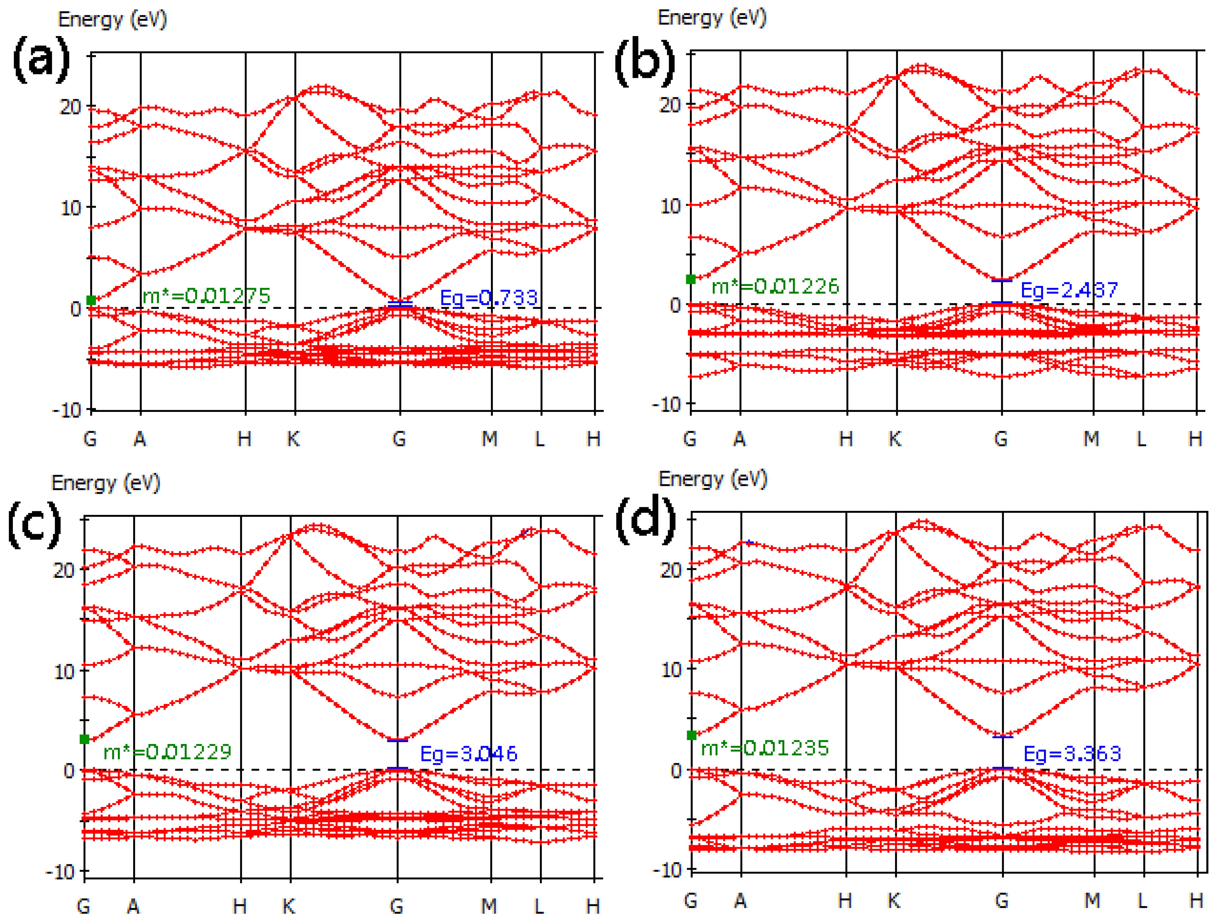
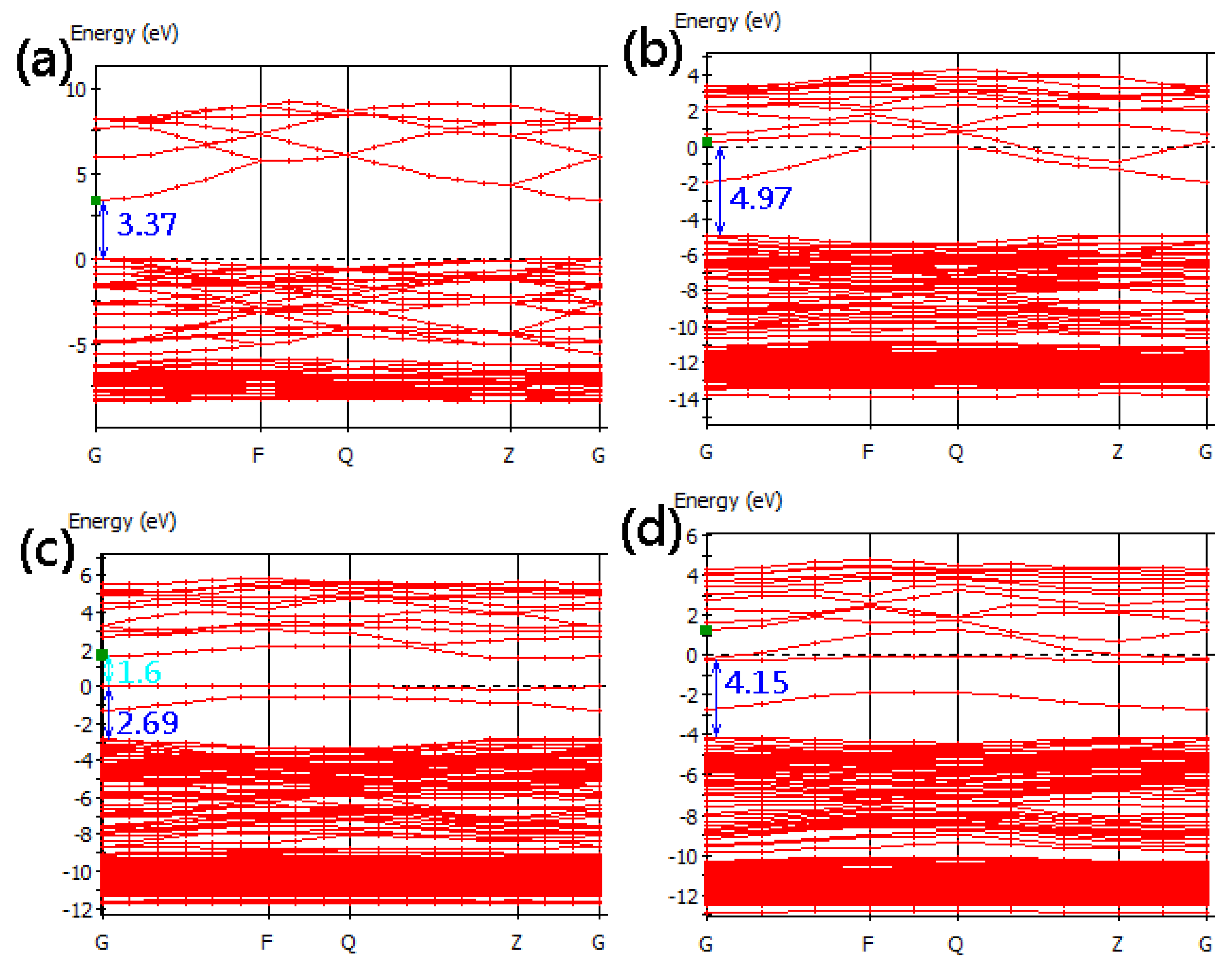
3.2. Band Structure

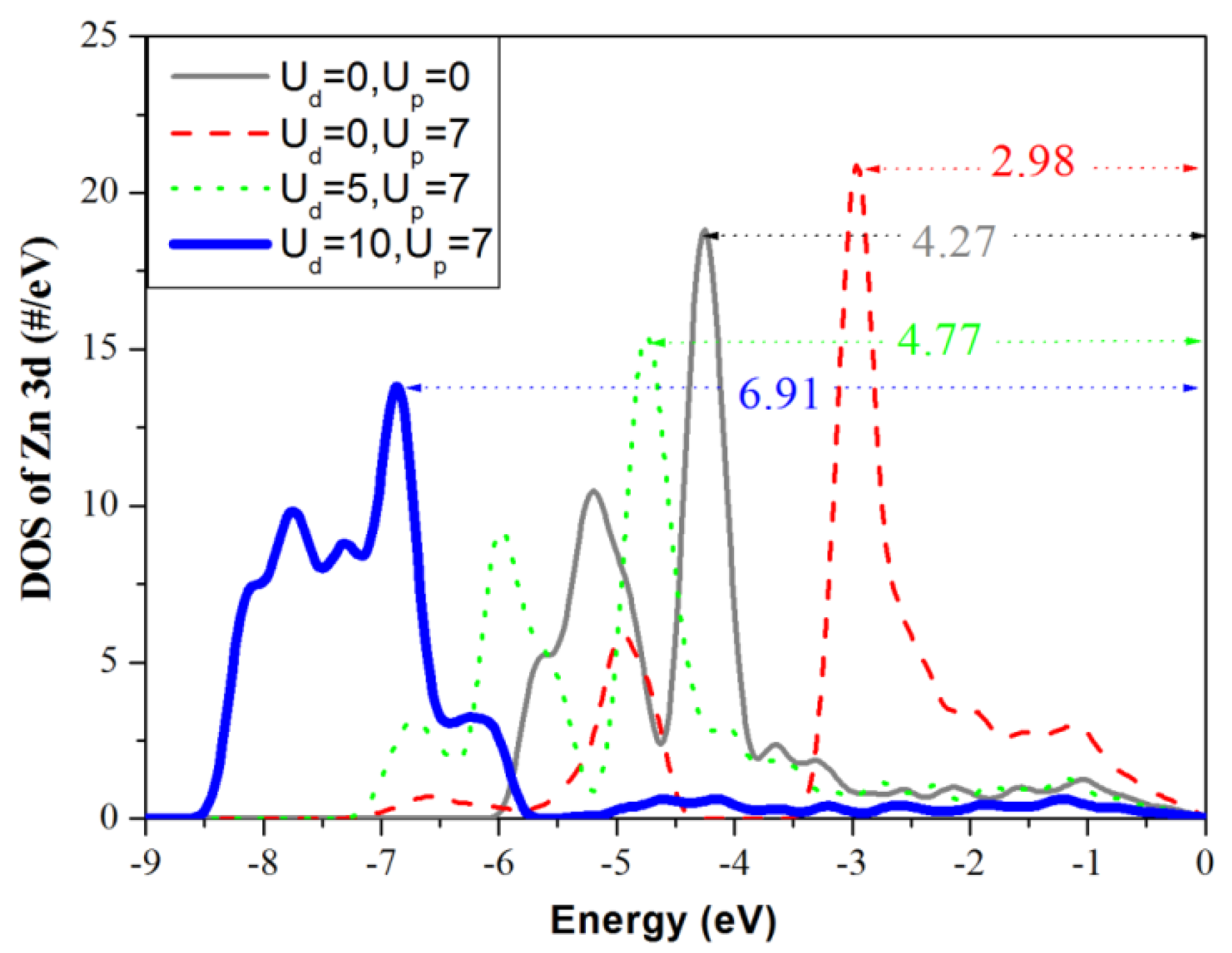
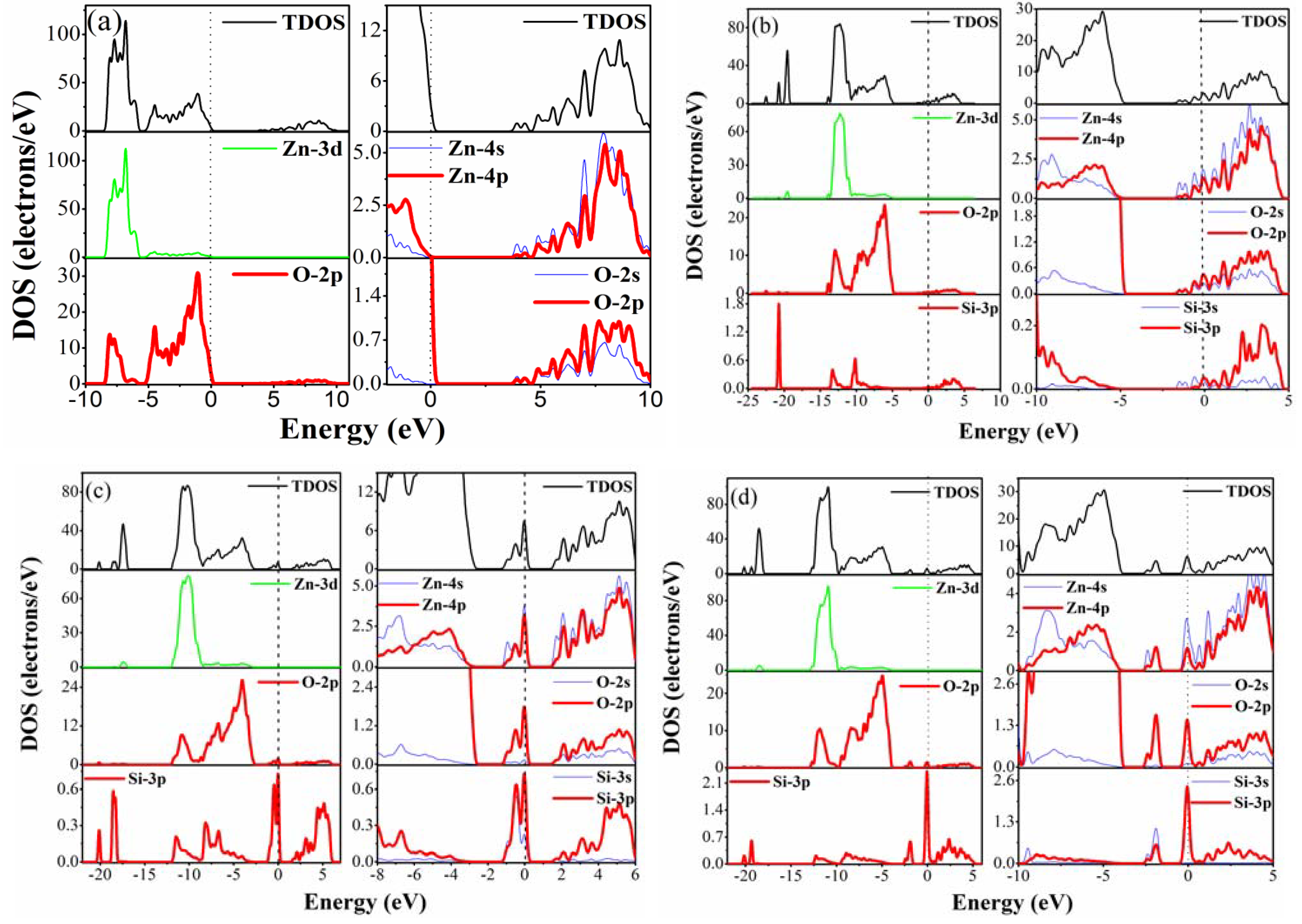
3.3. Density of States

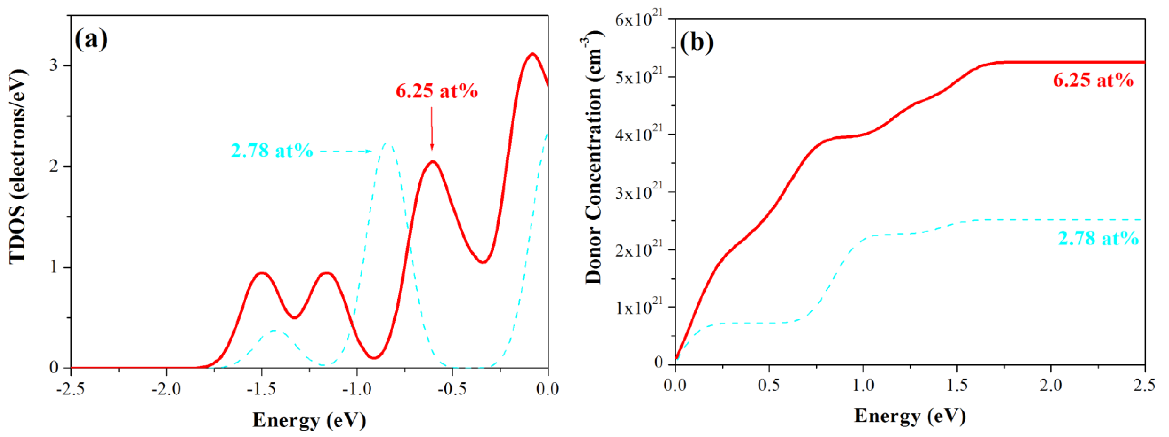
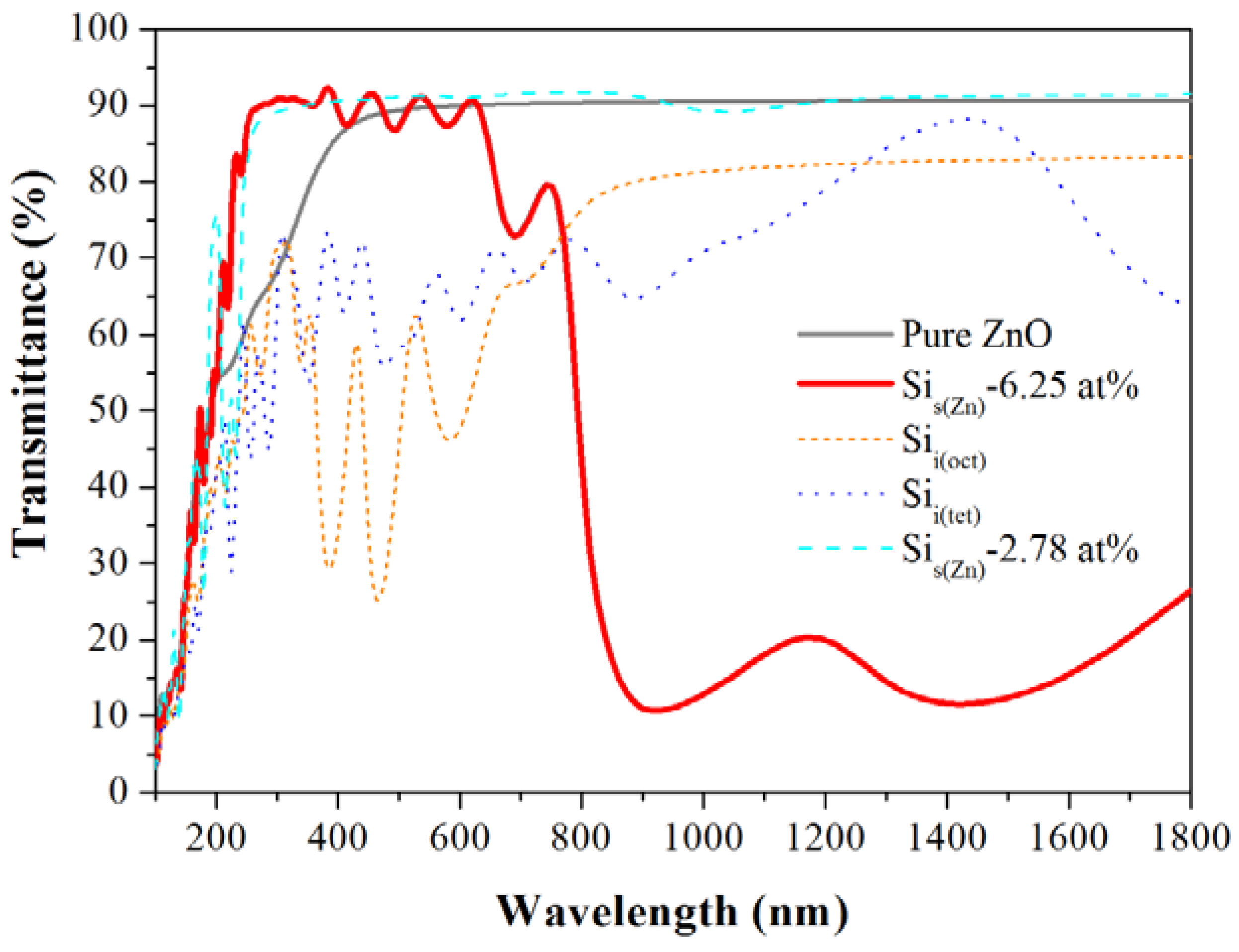
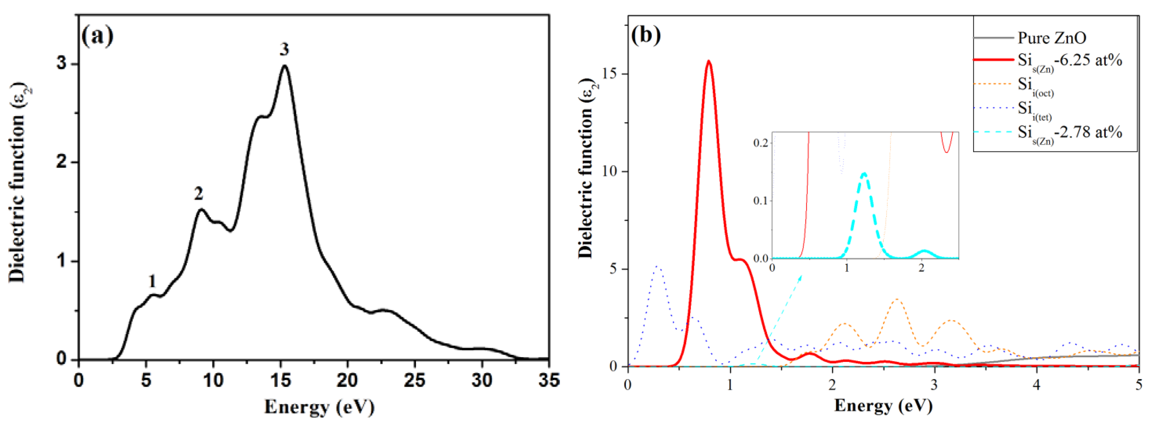
3.4. Optical Properties

4. Conclusions
Acknowledgments
References
- Vispute, R.D.; Talyansky, V.; Choopun, S.; Sharma, R.P.; Venkatesan, T.; He, M.; Tang, X.; Halpern, J.B.; Spencer, M.G.; Li, Y.X.; Salamanca-Riba, L.G.; Lliadis, A.A.; Jones, K.A. Heteroepitaxy of ZnO on GaN and its implications for fabrication of hybrid optoelectronic devices. Appl. Phys. Lett. 1998, 73, 348–351. [Google Scholar] [CrossRef]
- Clatot, J.; Campet, G.; Zeinert, A.; Labrugère, C.; Nistor, M.; Rougier, A. Low temperature Si doped ZnO thin films for transparent conducting oxides. Sol. Energy Mater. Sol. Cells 2011, 95, 2357–2362. [Google Scholar] [CrossRef]
- Wager, J.F. Transparent electronics. Science 2003, 300, 1245–1246. [Google Scholar] [CrossRef] [PubMed]
- Lu, M.P.; Lu, M.Y.; Chen, L.J. p-Type ZnO nanowires: From synthesis to nanoenergy. Nano Energy 2012, 1, 247–258. [Google Scholar] [CrossRef]
- Wu, K.; Gu, S.; Tang, K.; Ye, J.; Zhu, S.; Zhou, M.; Huang, Y.; Xu, M.; Zhang, R.; Zheng, Y. Temperature-dependent magnetization in (Mn, N)-codoped ZnO-based diluted magnetic semiconductors. J. Magn. Magn. Mater. 2012, 324, 1649–1654. [Google Scholar] [CrossRef]
- Zhang, Q.; Dandeneau, C.S.; Zhou, X.; Cao, G. ZnO Nanostructures for dye-sensitized solar cells. Adv. Mater. 2009, 21, 4087–4108. [Google Scholar] [CrossRef]
- Kim, Y.S.; Tai, W.P. Electrical and optical properties of Al-doped ZnO thin films by sol-gel process. Appl. Surf. Sci. 2007, 253, 4911–4916. [Google Scholar] [CrossRef]
- Tsay, C.Y.; Wu, C.W.; Lei, C.M.; Chen, F.S.; Lin, C.K. Microstructural and optical properties of Ga-doped ZnO semiconductor thin films prepared by sol–gel process. Thin Solid Films 2010, 519, 1516–1520. [Google Scholar] [CrossRef]
- Lucio-lópez, M.A.; Luna-arias, M.A.; Maldonado, A.; Olvera, M.; de la, L.; Acosta, D.R. Preparation of conducting and transparent indium-doped ZnO thin films by chemical spray. Sol. Energy Mater. Sol. Cells 2006, 90, 733–741. [Google Scholar] [CrossRef]
- Chang, H.P.; Wang, F.H.; Chao, J.C.; Huang, C.C.; Liu, H.W. Effects of thickness and annealing on the properties of Ti-doped ZnO films by radio frequency magnetron sputtering. Curr. Appl. Phys. 2011, 11, S185–S190. [Google Scholar] [CrossRef]
- Paul, G.K.; Bandyopadhyay, S.; Sen, S.K.; Sen, S. Structural, optical and electrical studies on sol-gel deposited Zr doped ZnO films. Mater. Chem. Phys. 2003, 79, 71–75. [Google Scholar] [CrossRef]
- Zhao, J.; Qin, L.; Zhang, L. Synthesis of quasi-aligned Si-doped ZnO nanorods on Si substrate. Physica E 2008, 40, 795–799. [Google Scholar] [CrossRef]
- Minami, T.; Sato, H.; Nanto, H.; Takata, S. Highly conductive and transparent sillicon doped zinc oxide thin films prepared by RF magnetron sputtering. Jpn. J. Appl. Phys. 1986, 25, L776–L779. [Google Scholar] [CrossRef]
- Das, A.K.; Misra, P.; Kukreja, L.M. Effect of Si doping on electrical and optical properties of ZnO thin films grown by sequential pulsed laser deposition. J. Phys. D: Appl. Phys. 2009, 42, 165405:1–165405:7. [Google Scholar]
- Luo, J.T.; Zhu, X.Y.; Chen, G.; Zeng, F.; Pan, F. The electrical, optical and magnetic properties of Si-doped ZnO films. Appl. Surf. Sci. 2012, 258, 2177–2181. [Google Scholar] [CrossRef]
- Sorar, I.; Saygin-Hinczewski, D.; Hinczewski, M.; Tepehan, F.Z. Optical and structural properties of Si-doped ZnO thin films. Appl. Surf. Sci. 2011, 257, 7343–7349. [Google Scholar] [CrossRef]
- Sato, H.; Minami, T.; Takata, S. Highly transparent and conductive group IV impurity-doped ZnO thin films prepared by radio frequency magnetron sputtering. J. Vac. Sci. Technol. A 1993, 11, 2975–2979. [Google Scholar] [CrossRef]
- Nomoto, J.; Miyata, T.; Minami, T. Transparent conducting Si-codoped Al-doped ZnO thin films prepared by magnetron sputtering using Al-doped ZnO powder targets containing SiC. J. Vac. Sci. Technol. A 2009, 27, 1001–1005. [Google Scholar] [CrossRef]
- Körner, W.; Elsässer, C. Density functional theory study for polycrystalline ZnO doped with Si or Nb. Phys. Rev. B 2011, 83, 205306:1–205306:6. [Google Scholar]
- Chowdhury, R.; Rees, P.; Adhikari, S.; Scarpa, F.; Wilks, S.P. Electronic structures of silicon doped ZnO. Physica B 2010, 405, 1980–1985. [Google Scholar] [CrossRef]
- Chowdhury, R.; Adhikari, S.; Rees, P. Optical properties of silicon doped ZnO. Physica B 2010, 405, 4763–4767. [Google Scholar] [CrossRef]
- Ma, X.; Lu, B.; Li, D.; Shi, R.; Pan, C.; Zhu, Y. Origin of photocatalytic activation of silver orthophosphate from First-principles. J. Phys. Chem. C 2011, 115, 4680–4687. [Google Scholar] [CrossRef]
- Ma, X.; Wu, Y.; Lu, Y.; Xu, J.; Wang, Y.; Zhu, Y. Effect of compensated codoping on the photoelectrochemical properties of Anatase TiO2 photocatalyst. J. Phys. Chem. C 2011, 115, 16963–16969. [Google Scholar] [CrossRef]
- Sheetz, R.M.; Ponomareva, I.; Richter, E.; Andriotis, A.N.; Menon, M. Defect-induced optical absorption in the visible range in ZnO nanowires. Phy. Rev. B 2009, 80, 195314:1–195314:4. [Google Scholar] [CrossRef]
- Segall, M.D.; Lindan, P.J.D.; Probert, M.J.; Pickard, C.J.; Hasnip, P.J.; Clark, S.J.; Payne, M.C. First-principles simulation: Ideas, illustrations and the CASTEP code. J. Phys. Condens. Matter 2002, 14, 2717–2744. [Google Scholar] [CrossRef]
- Vanderbilt, D. Soft self-consistent pseudopotentials in a generalized eigenvalue formalism. Phys. Rev. B 1990, 41, 7892–7895. [Google Scholar] [CrossRef]
- Monkhorst, H.J.; Pack, J.D. Special points for Brillouin-zone integrations. Phys. Rev. B 1976, 13, 5188–5192. [Google Scholar] [CrossRef]
- Oba, F.; Choi, M.; Togo, A.; Tanaka, I. Point defects in ZnO: An approach from first principles. Sci. Technol. Adv. Mater. 2011, 12. [Google Scholar] [CrossRef]
- Uddin, J.; Scuseria, G.E. Theoretical study of ZnO phases using a screened hybrid density functional. Phys. Rev. B 2006, 74, 245115:1–245115:7. [Google Scholar] [CrossRef]
- Hengehold, R.L.; Almassy, R.J.; Pedrotti, F.L. Electron energy-loss and ultraviolet-reflectivity spectra of crystalline ZnO. Phy. Rev. B 1970, 1, 4784–4791. [Google Scholar] [CrossRef]
© 2012 by the authors; licensee MDPI, Basel, Switzerland. This article is an open access article distributed under the terms and conditions of the Creative Commons Attribution license (http://creativecommons.org/licenses/by/4.0/).
Share and Cite
Wu, H.-C.; Peng, Y.-C.; Shen, T.-P. Electronic and Optical Properties of Substitutional and Interstitial Si-Doped ZnO. Materials 2012, 5, 2088-2100. https://doi.org/10.3390/ma5112088
Wu H-C, Peng Y-C, Shen T-P. Electronic and Optical Properties of Substitutional and Interstitial Si-Doped ZnO. Materials. 2012; 5(11):2088-2100. https://doi.org/10.3390/ma5112088
Chicago/Turabian StyleWu, Hsuan-Chung, Yen-Chun Peng, and Tsu-Ping Shen. 2012. "Electronic and Optical Properties of Substitutional and Interstitial Si-Doped ZnO" Materials 5, no. 11: 2088-2100. https://doi.org/10.3390/ma5112088