2.1. Crystal structure and XRD patterns
Generally, the crystal structure of (
MS)
1+x(TiS
2)
2 is composed of a layer of
MS sandwiched between two TiS
2 layers with a van der Waals gap [
3]. The crystal structure of (PbS)
1.18(TiS
2)
2 has been refined from XRD data [
7] and is shown in
Figure 1. The Pb and S(1) atom of the PbS subsystem are in 4(
i) sites of space group C2/m; each Pb atom is coordinated by five S atoms located at the corners of a slightly distorted square pyramid (NaC1 structure type). As Pb atoms protrude from the sulfur planes on both sides, each Pb atom is also bonded to two or three S atoms of the TiS
2 slabs by weak covalent force. The atoms of the (TiS
2)
2 subsystem are on 2(
e) sites of space group C2
1/m. Each Ti atom is coordinated by six S atoms in a trigonal antiprismatic arrangement. The (TiS
2)
2 slab is slightly distorted compared with 1
T-TiS
2 ,in which Ti is octahedrally coordinated. It is seen that the stacking of the two adjacent TiS
2 sandwiches are the same as in l
T-TiS
2.
The XRD patterns of the surfaces of the (
MS)
1+x(TiS
2)
2 sintered bodies perpendicular to the pressing direction are shown in
Figure 2. Sharp (0 0
l) peaks which correspond to the planes perpendicular to the
c-axis can be observed and very few (
h k l) planes are detected, showing that the
c-axes are preferentially oriented along the pressing direction. The atomic bondings in these misfit layer compounds are highly anisotropic, and the atomic bondings within the layers must be strong due to high covalency and the interlayer bonding formed mainly by van der Waals force is very weak. Under the pressure during SPS sintering, the crystals tend to slide along the layers and deflect until the layers become aligned perpendicular to the pressure, thereby resulting in high preferred-orientation of the (0 0
l) planes. Rocking curve is also measured to characterize the degree of preferred orientation. It shows that the full width at half maximum (FWHM) of the (0 0 12) peak of (BiS)
1.18(TiS
2)
2, (SnS)
1.2(TiS
2)
2 and (PbS)
1.18(TiS
2)
2 are 17.6°, 15.1° and 17.2° respectively. Although the values are not as low as those of the films, the degree of preferred orientation for the (0 0
l) planes of these polycrystalline samples is high enough to approach the in-plane transport prosperities of a single crystal. There are some minor peaks between 20°-30° in (PbS)
1.18(TiS
2)
2 and (SnS)
1.2(TiS
2)
2, which may have arisen from the stage-1 compounds (PbS)
1.18TiS
2 and (SnS)
1.2TiS
2, but their presence should have little influence on the thermoelectric properties because their content is negligible.
Figure 1.
Crystal structure of (PbS)1.18(TiS2)2 along the incommensurate direction.
Figure 1.
Crystal structure of (PbS)1.18(TiS2)2 along the incommensurate direction.
Figure 2.
XRD patterns of (BiS)1.2(TiS2)2, (SnS)1.2(TiS2)2 and (PbS)1.18(TiS2)2.
Figure 2.
XRD patterns of (BiS)1.2(TiS2)2, (SnS)1.2(TiS2)2 and (PbS)1.18(TiS2)2.
2.2. Electrical properties
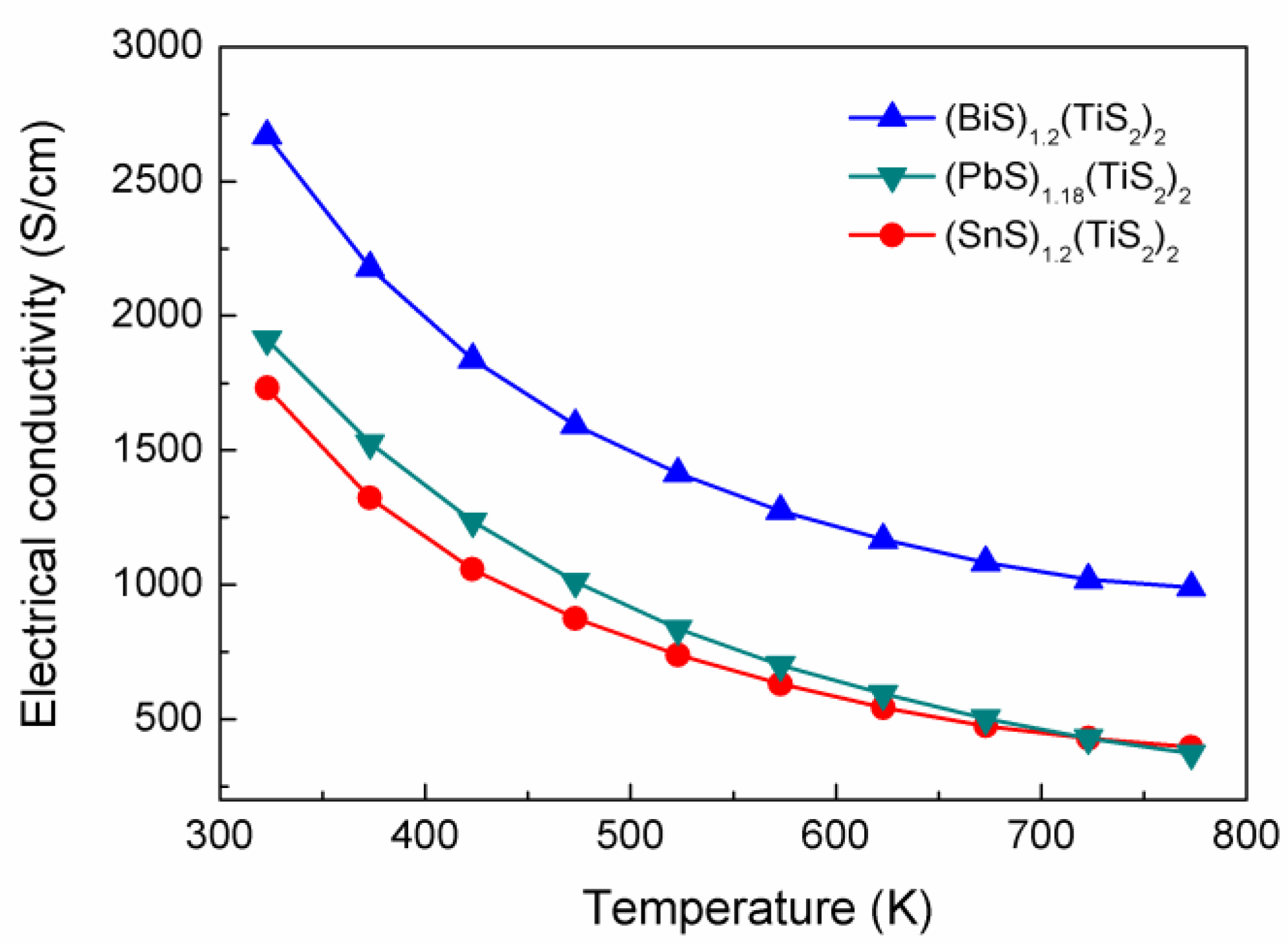
As shown in
Figure 3, all the (BiS)
1.2(TiS
2)
2, (SnS)
1.2(TiS
2)
2 and (PbS)
1.18(TiS
2)
2 compounds show metallic electrical conductivities of the order of 1,700~2,700 S/cm at room temperature. The electrical conductivity decreases in the sequence of Bi, Pb, Sn for (
MS)
1+x(TiS
2)
2 over the whole temperature range.
Figure 3.
Electrical conductivities of (BiS)1.2(TiS2)2, (SnS)1.2(TiS2)2 and (PbS)1.18(TiS2)2.
Figure 3.
Electrical conductivities of (BiS)1.2(TiS2)2, (SnS)1.2(TiS2)2 and (PbS)1.18(TiS2)2.
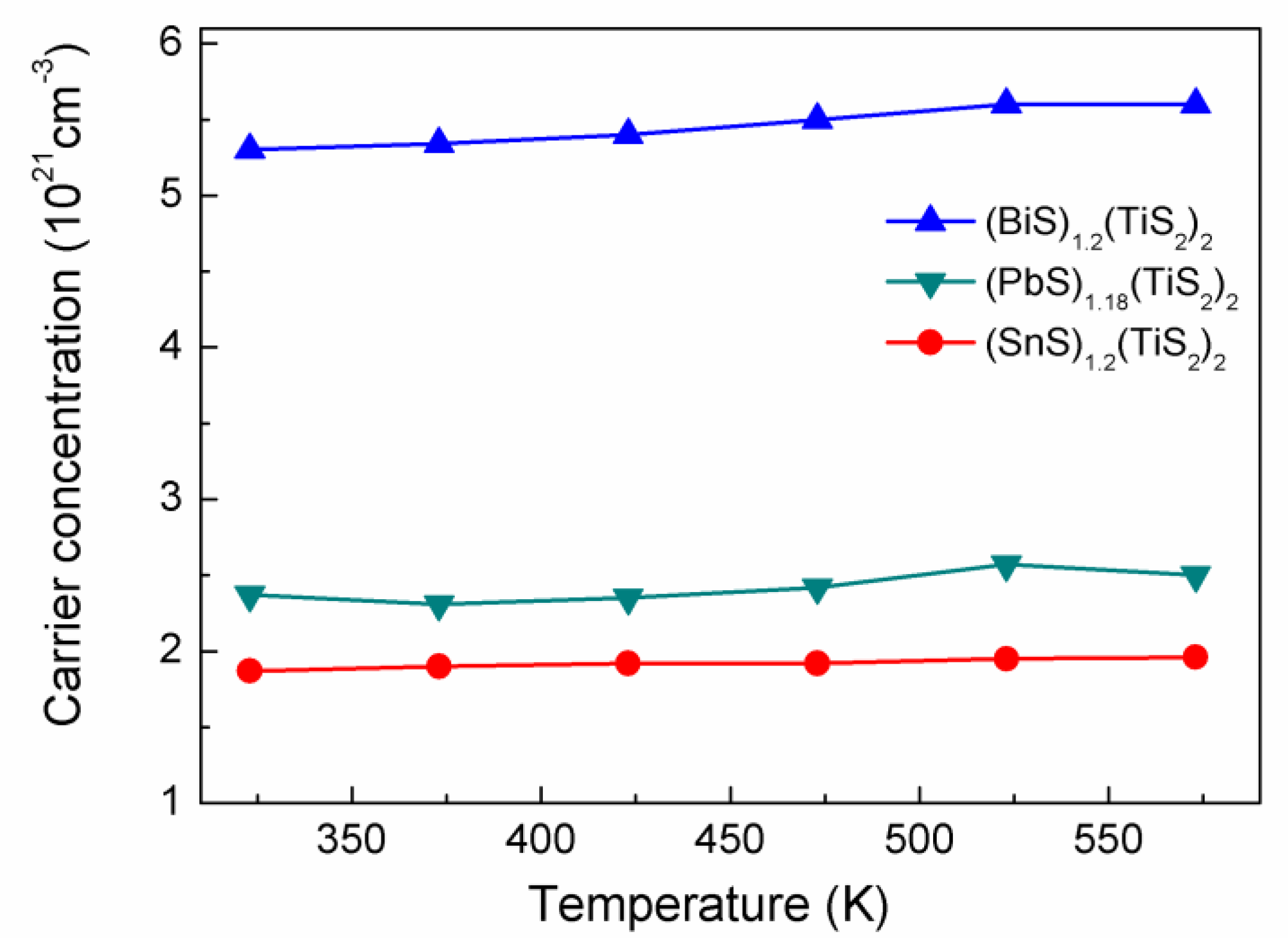
The electrical conductivity of materials is determined by the carrier concentration and mobility. Hall measurement was performed to analyze the electron transport properties in these misfit layer compounds. The Hall coefficients are all negative, showing that the dominant carriers in these compounds are electrons. As shown in
Figure 4, all the compositions show high carrier concentrations which are almost temperature independent, supporting the metallic conduction mechanism. For the (
MS)
1+x(TiS
2)
2 compositions, the carrier concentration decreases in the sequence of Bi, Sn, Pb which is consistent with the tendency of electrical conductivity. It has been known that pure TiS
2 is a small-bandgap semiconductor and the carrier concentration is 2.8 × 10
20 cm
-3 at room temperature [
4]. Since the misfit layer compound can be viewed as composite lattice of the
MS layer and the TiS
2 layer, the large carrier concentrations of the misfit layer compounds are believed to originate from electron transfer from the
MS layer to the TiS
2 layer [
3]. From the carrier concentrations and the lattice parameters, we can estimate the number of electrons per Ti atom received for (BiS)
1.2(TiS
2)
2, (SnS)
1.2(TiS
2)
2 and (PbS)
1.18(TiS
2)
2 is 0.45, 0.16 and 0.2, respectively. Much more electron transfer takes place in (BiS)
1.2(TiS
2)
2 than the other two compositions, because the valence of bismuth is 3+ here and one can easily deduce that one electron can be transferred from one BiS layer to two TiS
2 layers, leading to that each Ti atom receive 0.6 electrons, which is in reasonable agreement with the above estimation.
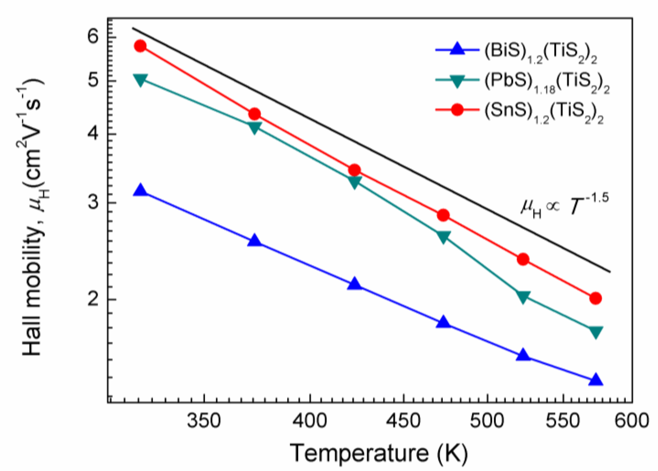
The Hall mobilities for the (
MS)
1+x(TiS
2)
2 compositions are plotted in
Figure 5. The mobilities for all the compositions have temperature dependences proportional to
T -1.5, showing that the electrons are mainly scattered by acoustic phonons. The degree of orientation of the (0 0
l) planes in these polycrystalline samples may affect the mobility, as the electron mobility is much lower in the cross-plane direction of these misfit layer compounds [
8]. However, the similar FWHM of the rocking curve shows that the degree of orientation is close for these three compositions and its effect on the mobility is limited.
Figure 4.
Carrier concentrations of (BiS)1.2(TiS2)2, (SnS)1.2(TiS2)2 and (PbS)1.18(TiS2)2.
Figure 4.
Carrier concentrations of (BiS)1.2(TiS2)2, (SnS)1.2(TiS2)2 and (PbS)1.18(TiS2)2.
Figure 5.
Hall mobilities for (BiS)1.2(TiS2)2, (SnS)1.2(TiS2)2 and (PbS)1.18(TiS2)2.
Figure 5.
Hall mobilities for (BiS)1.2(TiS2)2, (SnS)1.2(TiS2)2 and (PbS)1.18(TiS2)2.
The mobility in the (MS)1+x(TiS2)2 decreases in the order of Sn > Pb > Bi which is almost opposite to that of carrier concentration. The electron transfer from the MS layers to the TiS2 layers may also change the effective mass, resulting in different mobilities. An estimation of the effective mass will be shown below.
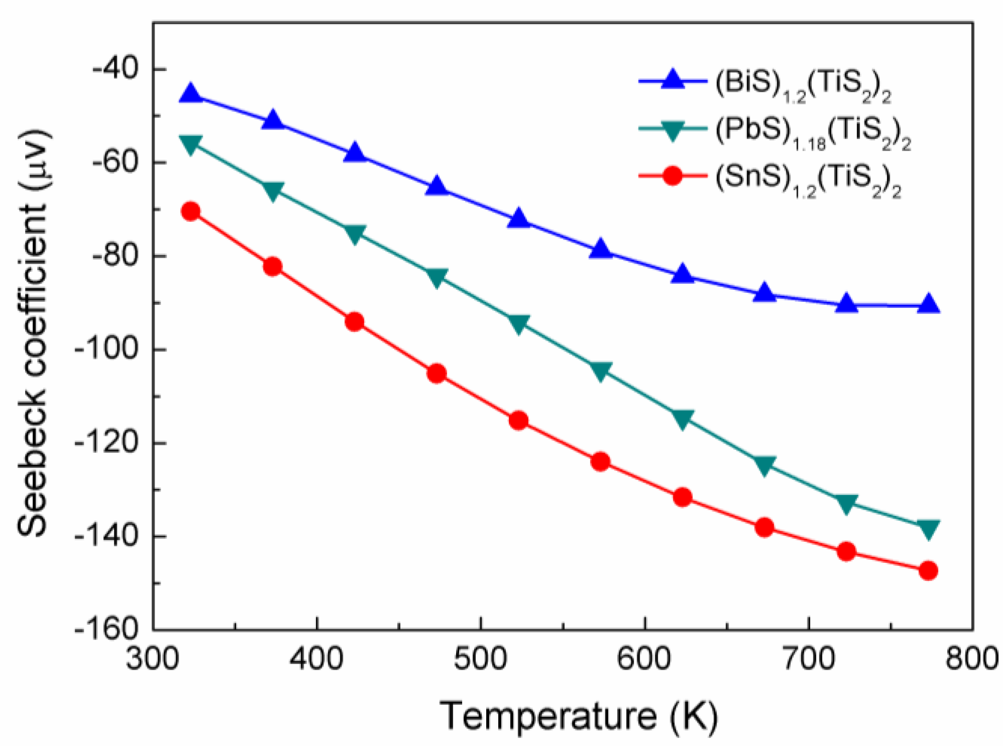
The (
MS)
1+x(TiS
2)
2 compositions show a relatively large Seebeck coefficient, as shown in
Figure 6. It can also be seen that the absolute Seebeck coefficient decreases in the order of Sn>Pb>Bi. In these intercalation compounds, electrical properties can be described by a rigid band model, which means that the only change in the electronic structure of the host is a change in a degree of band filling due to electron donation from the intercalated species to the host [
9]. It is realized that the
d orbitals of Ti plays an important role in determining the physical properties of TiS
2-based materials and the degree of band filling, their energy levels and the width of the
d-band significantly affect their thermoelectric properties [
9]. Accordingly, the Seebeck coefficient decreasing in the order of Sn>Pb>Bi strongly suggests an increase in the number of electrons per Ti atom received, namely indicating higher degree of band filling was achieved.
Figure 6.
Seebeck coefficients of (BiS)1.2(TiS2)2, (SnS)1.2(TiS2)2 and (PbS)1.18(TiS2)2.
Figure 6.
Seebeck coefficients of (BiS)1.2(TiS2)2, (SnS)1.2(TiS2)2 and (PbS)1.18(TiS2)2.
The density-of-states (DOS) effective mass,
m*, one of the main factors determining
S, were estimated by the use of the following equations [
10]:
where
h,
kB,
ne,
Fn and
ξ are the Plank constant, the Boltzmann constant, the carrier concentration, the Fermi integral, and the chemical potential, respectively.
Fn(
ξ) and
S can be expressed as [
10]:
where
e is the electron charge, and
r is the carrier scattering parameter of relaxation time which was assumed to be
r = 0 since the carriers are scattered only by acoustic phonons. The
m* values for (BiS)
1.2(TiS
2)
2, (SnS)
1.2(TiS
2)
2 and (PbS)
1.18(TiS
2)
2 were calculated to be 6.3
m0, 4.8
m0 and 4.5
m0, respectively, where
m0 is the bare electron mass. It can be seen that (BiS)
1.2(TiS
2)
2 has the highest effective mass, resulting in the lowest mobility as shown in
Figure 5.
As shown in
Figure 7, the power factors of the (
MS)
1+x(TiS
2)
2 compositions fall within the range of 5 × 10
-4 to 10
-3 W/K
2m, which is much lower than the conventional thermoelectric material Bi
2Te
3 (~5 × 10
-3 W/K
2m). At lower temperatures, the power factors almost increase in the order of Bi < Pb < Sn, indicative of increased carrier concentration. Although the carrier concentration in (
MS)
1+x(TiS
2)
2 is not yet optimized, it can be expected that further reduction in carrier concentration would increase the power factor. Acceptor doping may be employed to reduce the carrier concentration as in the case of TiS
2 doped with Mg and Cd [
11,
12].
Figure 7.
Power factors of (BiS)1.2(TiS2)2, (SnS)1.2(TiS2)2 and (PbS)1.18(TiS2)2.
Figure 7.
Power factors of (BiS)1.2(TiS2)2, (SnS)1.2(TiS2)2 and (PbS)1.18(TiS2)2.
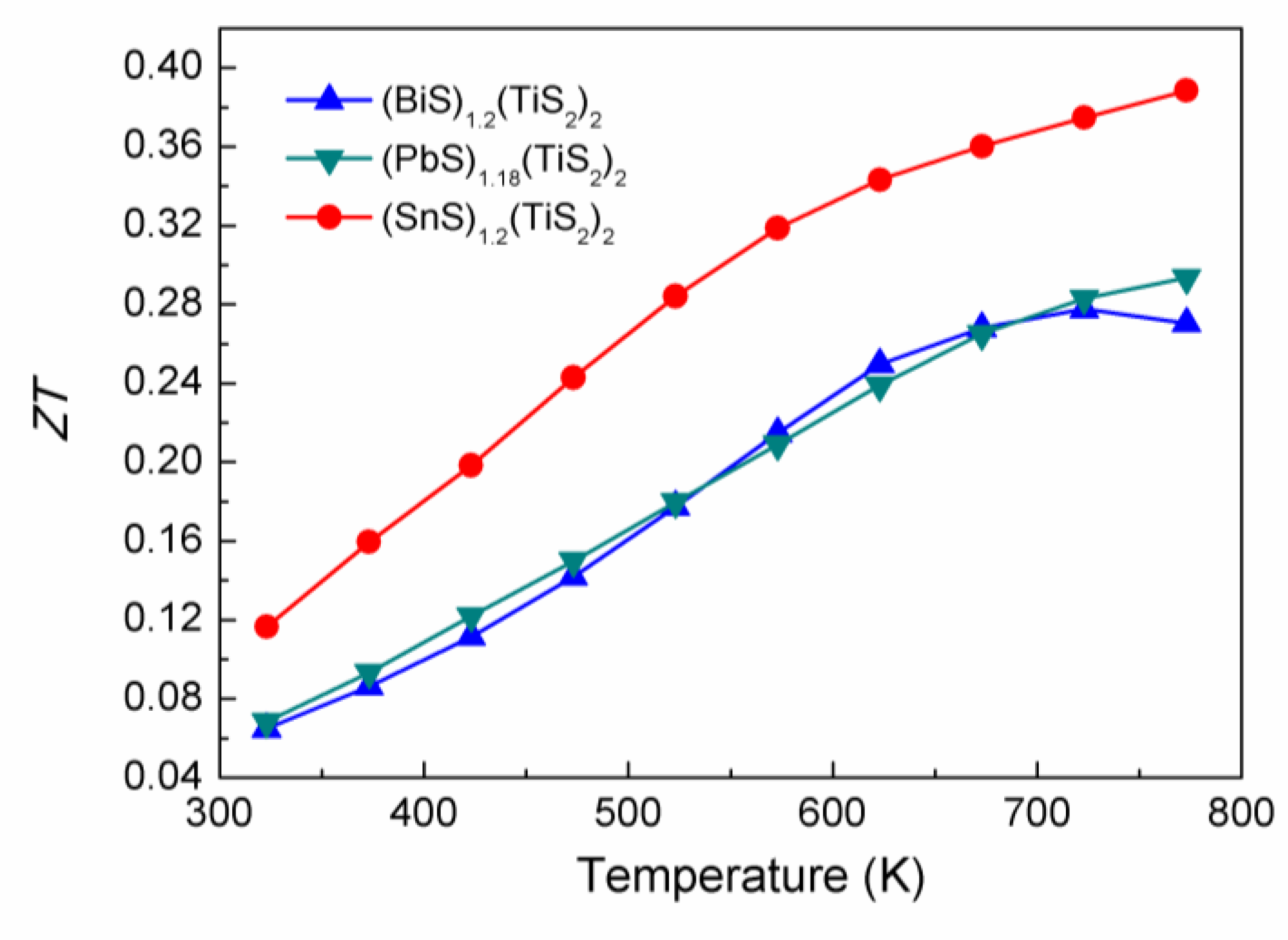
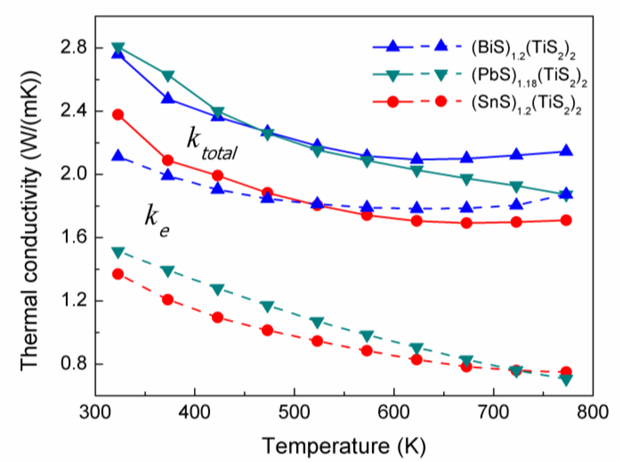
2.3. Thermal conductivity
As shown in
Figure 8, the (
MS)
1+x(TiS
2)
2 compositions exhibit relatively low thermal conductivity. (SnS)
1.2(TiS
2)
2 has lower thermal conductivity than the other compositions in the whole temperature range. Since the thermal conductivity comes from two sources: (1) electrons and holes transporting heat (
ke) and (2) phonons travelling through the lattice (
kl), the electronic thermal conductivity (
ke) is directly related to the electrical conductivity through the Wiedemann-Franz law:
ke=
L0Tσ, where the Lorenz number
L0 is 2.44 × 10
-8 J
-2C
-2K
-2. The values of
ke of these (
MS)
1+x(TiS
2)
2 compositions were calculated and plotted in
Figure 8. It can be seen that
ke largely contributes to the total thermal conductivity, especially in (BiS)
1.2(TiS
2)
2. (SnS)
1.2(TiS
2)
2 has the lowest carrier concentration and electrical conductivity, resulting in the lowest
ke and also the lowest
ktotal.
Figure 8.
Total thermal conductivities (ktotal, solid line) and electron thermal conductivities (ke, dashed line) of (BiS)1.2(TiS2)2, (SnS)1.2(TiS2)2 and (PbS)1.18(TiS2)2.
Figure 8.
Total thermal conductivities (ktotal, solid line) and electron thermal conductivities (ke, dashed line) of (BiS)1.2(TiS2)2, (SnS)1.2(TiS2)2 and (PbS)1.18(TiS2)2.
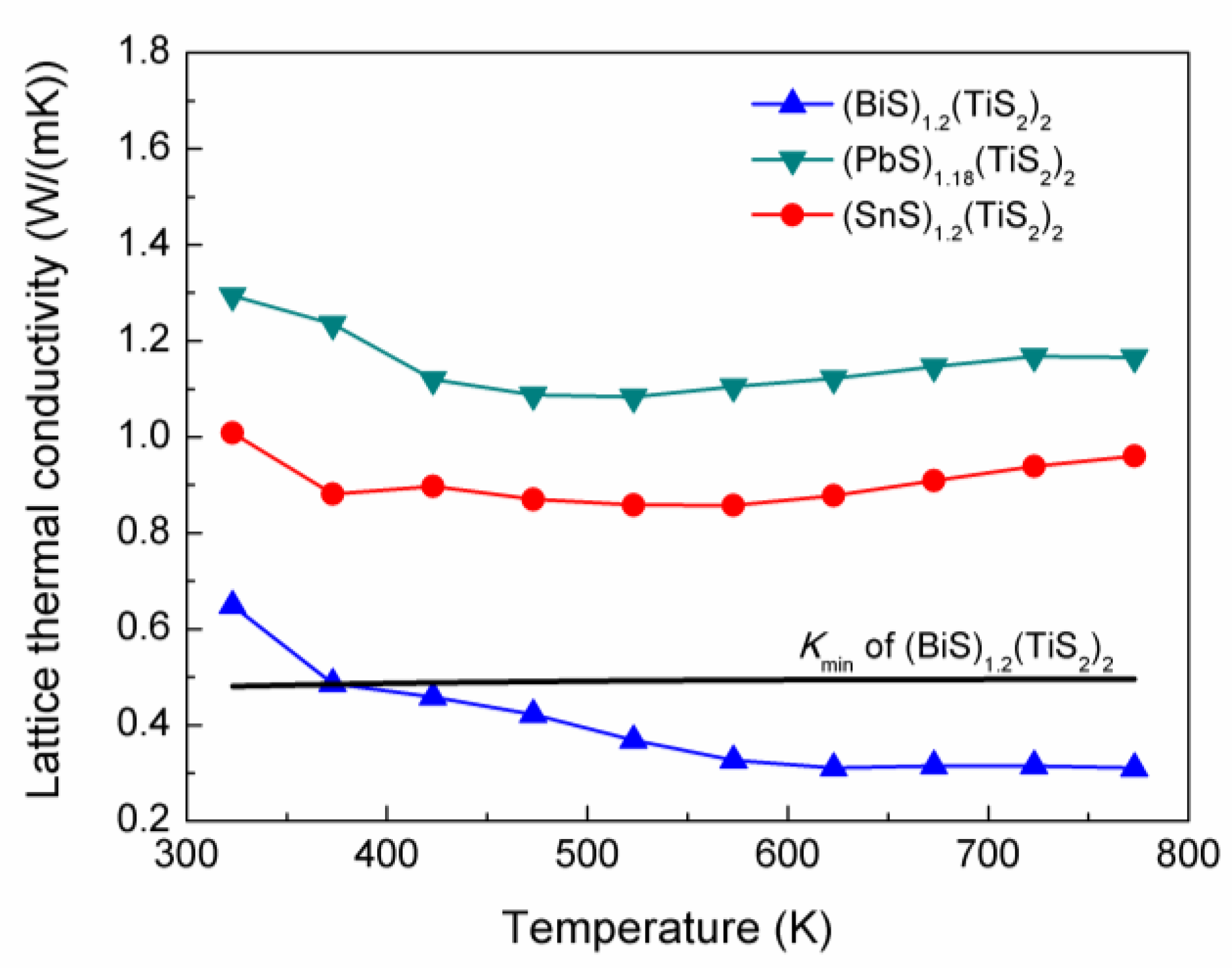
The lattice thermal conductivity was then calculated by subtracting
ke from
ktotal, which is shown in
Figure 9. It can be noticed that (
MS)
1+x(TiS
2)
2 has extremely low lattice thermal conductivity, which can be related to their modulated structure. (BiS)
1.2(TiS
2)
2 exhibits the lowest
kl and can even reach 0.3 W/mK around 700K. The minimum thermal conductivity can be calculated for this composition from the equation [
13]:
The sum is taken over the three sound modes including two transverse and one longitudinal modes with the speed of sound
vi.
θi is the Debye temperature for each polarization,
θi = υi(ħ/kB)6π2n)⅓, where
n is the number density of atoms [
13]. Using the measured values of
VL,
VT1,
VT2, the
kmin was calcuated and shown in
Figure 9.
kl of (BiS)
1.2(TiS
2)
2 is even lower than
kmin, which can hardly be observed in the bulk materials.
Figure 9.
Lattice thermal conductivities of (BiS)1.2(TiS2)2, (SnS)1.2(TiS2)2 and (PbS)1.18(TiS2)2. The calculated minimum thermal conductivity for (BiS)1.2(TiS2)2 is also included.
Figure 9.
Lattice thermal conductivities of (BiS)1.2(TiS2)2, (SnS)1.2(TiS2)2 and (PbS)1.18(TiS2)2. The calculated minimum thermal conductivity for (BiS)1.2(TiS2)2 is also included.
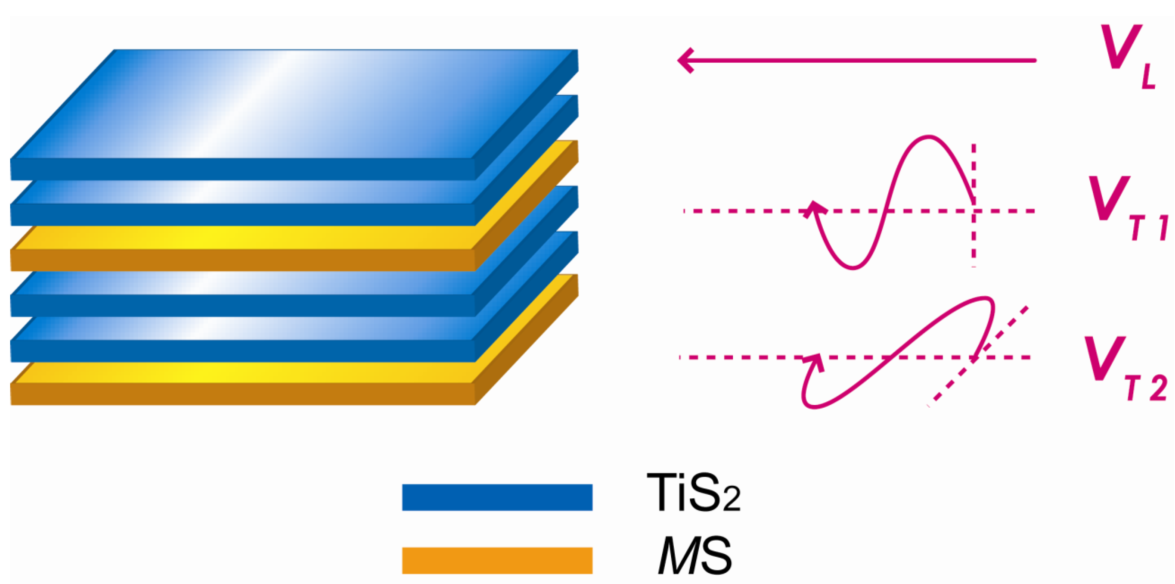
To analyze the ultra-low thermal conductivity, the kinetic theory of thermal conductivity was used:
where
Cv,
l and
V represent the heat capacity, phonon mean free path and speed of sound, respectively. The heat capacity makes limited contribution to the low thermal conductivity, as the heat capacity approaches 3
kB per atom at temperatures higher than the Debye temperature, according to the Dulong-Petit law. The phonon mean free path is restricted by various phonon scattering processes. The present study focused on the the sound velocity which is determined by the density and the elastic constant of a solid. The sound velocity has three polarizations, including one longitudinal mode and two transverse modes, as shown in
Figure 10.
A pulse-echo method was used to measure these sound velocities with a 30 MHz longitudinal transducer and a 20 MHz transverse transducer. The measured values are listed in
Table 1. The corresponding values for TiS
2 are also included for comparison.
Figure 10.
Schematic illustration of the longitudinal and transverse sound velocities of the layered (MS)1+x(TiS2)2 compounds.
Figure 10.
Schematic illustration of the longitudinal and transverse sound velocities of the layered (MS)1+x(TiS2)2 compounds.
Table 1.
Densities, longitudinal and transverse sound velocities, and shear moduli of TiS2, (BiS)1.2(TiS2)2, (SnS)1.2(TiS2)2 and (PbS)1.18(TiS2)2.
Table 1.
Densities, longitudinal and transverse sound velocities, and shear moduli of TiS2, (BiS)1.2(TiS2)2, (SnS)1.2(TiS2)2 and (PbS)1.18(TiS2)2.
| Material | ρ
g/cm3 | VL
m/s | VT1
m/s | VT2
m/s | G1
GPa | G2
GPa |
|---|
| TiS2 | 3.21 | 5284 | 2799 | 3295 | 25.0 | 34.7 |
| (BiS)1.2(TiS2)2 | 4.57 | 3662 | 1350 | 1688 | 8.3 | 13.0 |
| (PbS)1.18(TiS2)2 | 4.69 | 3834 | 1120 | 1837 | 5.9 | 15.8 |
| (SnS)1.2(TiS2)2 | 3.87 | 4111 | 1578 | 2352 | 9.6 | 21.4 |
Compared with pure TiS
2, the longitudinal velocities of the misfit layer compounds are a little decreased, which can be attributed to the increase of density. In contrast, the transverse sound velocities, especially
VT1, apparently decreased, which arises from the softening of atomic bonding. The transverse polarization is a kind of shear movement, and the velocity is determined by shear modulus as follows:
where
G is the shear modulus and
ρ is the density. The shear modulus is calculated by the above equation and shown in
Table 1. The shear moduli of the misfit layer compounds are much lower than those of pure TiS
2 due to the intercalation of the
MS layers into the TiS
2 layers. It can also be seen that the velocities of the two transverse waves (
VT1 and
VT2) are different, as
VT1 is mainly determined by the interlayer bonding while
VT2 is determined by the intralayer bonding. For
VT1, the weak interlayer bonding between the
MS layer and TiS
2 layer arises either from the electrostatic interaction due to electron transfer between these layers or a weak covalent force between the
M atom and the sulfur atoms in the TiS
2 layers [
14,
15]. For
VT2, the intralayer bonding is weakened, possibly due to the incommensurate structure or disruption of periodicity of TiS
2 layers in the direction perpendicular to the layers by the intercalated
MS layers.
It has been shown that the sound velocity decreased in the misfit layer compounds due to the weakened bonding, which can partially account for their low thermal conductivity. However, further investigation is required to understand the compositional dependence of lattice thermal conductivity of the (MS)1+x(TiS2)2 compounds, which mainly differ in phonon mean free path. It is anticipated that the electron transfer may play a role in determining the phonon transport, because (BiS)1.2(TiS2)2 which has the most electron transfer exhibits the lowest lattice thermal conductivity.


