Nonvolatile Resistive Switching Memory Utilizing Cobalt Embedded in Gelatin


Institute of Microelectronics, Department of Electrical Engineering, National Cheng-Kung University, Tainan 701, Taiwan
*
Author to whom correspondence should be addressed.
Materials 2018, 11(1), 32; https://doi.org/10.3390/ma11010032
Submission received: 30 October 2017
/
Revised: 21 December 2017
/
Accepted: 21 December 2017
/
Published: 26 December 2017
(This article belongs to the Special Issue Selected Papers from IEEE ICICE 2017)
Abstract
:This study investigates the preparation and electrical properties of Al/cobalt-embedded gelatin (CoG)/ indium tin oxide (ITO) resistive switching memories. Co. elements can be uniformly distributed in gelatin without a conventional dispersion procedure, as confirmed through energy dispersive X-ray analyzer and X-ray photoelectron spectroscopy observations. With an appropriate Co. concentration, Co. ions can assist the formation of an interfacial AlOx layer and improve the memory properties. High ON/OFF ratio, good retention capability, and good endurance switching cycles are demonstrated with 1 M Co. concentration, in contrast to 0.5 M and 2 M memory devices. This result can be attributed to the suitable thickness of the interfacial AlOx layer, which acts as an oxygen reservoir and stores and releases oxygen during switching. The Co. element in a solution-processed gelatin matrix has high potential for bio-electronic applications.
1. Introduction
Gelatin has excellent film formation properties and biodegradability, as well as superior solubility in water. In addition, gelatin memory devices possess a good ON/OFF ratio in the atmospheric environment for 90 days [1]. However, gelatin memory devices suffer from poor switching cycle endurance.
Most organic memory devices use metallic nanoparticles blended into an organic host to improve their memory properties and operational stability [2,3,4,5]. Organic nanocomposites, by dispersing metal nanoparticles into organic matrixes, possess greatly enhanced mechanical, optical, and electrical properties. However, metal nanoparticle dispersion in organic matrixes can weaken the repeatability of devices due to strong inter-particle interactions and weak polymer nanoparticle interfacial interaction (nanoparticle agglomeration). Moreover, controlling the size of metal nanoparticles is difficult [1].
In this study, cobalt-embedded gelatin (CoG) was used as an organic insulator layer, which is a one-component system that considerably simplifies the device structure and fabrication process. Based on the Al/CoG/ITO device structure, three Co.:gelatin mole ratios (2:1, 1:1, and 0.5:1) were adopted in the experiments. Device performance improvements were summarized and analyzed. With appropriate Co. concentration, the redox reaction of Co. can assist in the formation of the interfacial AlOx layer and improve the memory properties. Compared with CoG 0.5 M and 2 M memory devices, CoG 1 M memory devices exhibit good device performance, being forming-free, with a sufficient ON/OFF ratio (larger than 105), relatively good switching cycles, and extrapolated retention properties exceeding 10 years. According to the electrical properties and material analyses, the sufficient thickness of the interfacial AlOx layer and the smooth dielectric thin film is related to an appropriate Co. concentration in the gelatin matrix, which further enhances switching cycle endurance and retention capability.
2. Results
Figure 1a–c shows the X-ray photoelectron spectroscopy (XPS) patterns obtained after 90 s of Ar+ ion sputtering, thereby representing the bulk layer of CoG 0.5, 1, and 2 M thin films, respectively. XPS quantitative analyses revealed that the atomic percentages of Co. were 6%, 8%, and 14% for CoG 0.5, 1, and 2 M thin films, respectively. The Co. concentration tendency in the energy-dispersive X-ray spectroscopy (EDS) element mapping is consistent with the XPS quantitative analyses.
The fitting of high-resolution N 1s XPS peaks shows the presence of pyrrolic-N, oxidized-N, and pyridinic-N [6], with a relatively high content of pyridinic-N and pyrrolic-N in the CoG thin film. The simulated characteristics of Co. 2p peaks were able to be divided into two peaks at around 781.5 eV and 797.4 eV, which confirmed the existence of Co2+ and Co3+ in the CoG thin films by XPS analysis [7,8]. The O 1s peaks were able to be divided into two peaks at 530 eV and 532 eV, which were assigned to lattice and non-lattice oxygen, respectively. The C 1s peaks were able to be divided into two peaks at 284 eV and 288 eV, which were assigned to epoxyl C–O and carboxyl O–C=O, respectively.
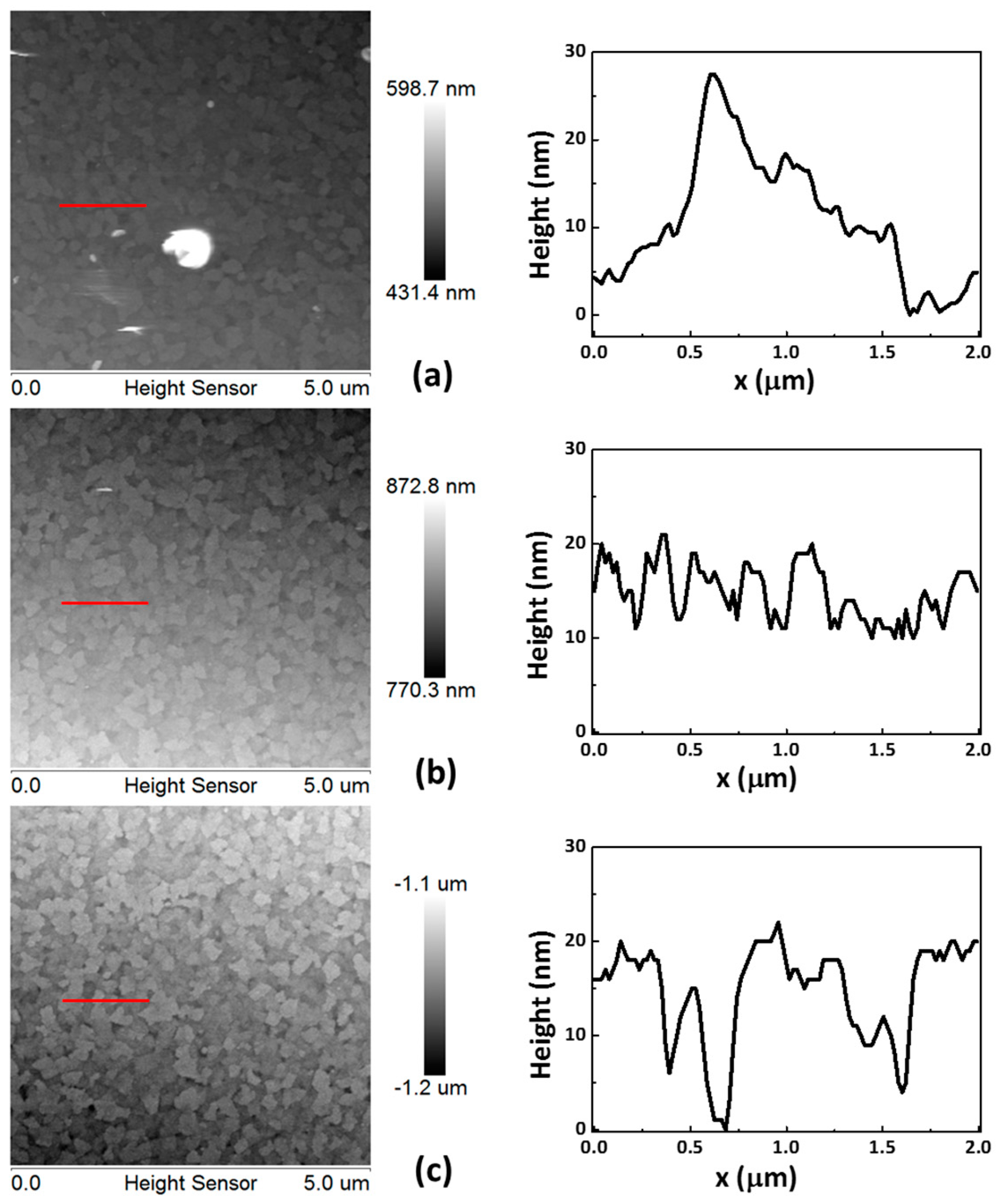
Figure 2a–c illustrates the surface topographies of the CoG 0.5, 1, and 2 M samples, respectively. The roughness values of the CoG 0.5, 1, and 2 M thin films are 5.1, 2.8, and 3.6 nm, respectively. These parameters confirm that CoG 1 M has the smoothest surface.
Figure 3a depicts the I–V characteristics of the Al/CoG 0.5 M/ITO, Al/CoG 1 M/ITO, and Al/CoG 2 M/ITO structures. Bipolar resistive switching behaviors are clearly observable. Similar to gelatin, the bipolar resistive switching behavior does not require an electroforming process. The forming voltage is usually far greater than the set voltage. In the CoG memory device case, the first and second I–V curves of the CoG 1 M memory device show nearly the same set voltage of around 1.3 V. Thus, a high-voltage forming process was avoided in the CoG memory device. Voltage series of 3 to −3 V, 4 to −4 V, and 5 to −5 V were used to operate the memory devices in this study. However, the voltage series of 3 V to −3V was insufficient to switch the device from a high-resistance state (HRS) to a low-resistance state (LRS). The voltage series of 5 V to −5 V has similar I–V characteristics with the voltage series of 4 V to −4 V. The switches can be operated with a smaller bias voltage of 4 V to −4 V, which may be preferable for memory devices with lower power consumption. Thus, the voltage was applied to the top Al electrode in a sequence of +4 V → 0 V → −4 V → 0 V → +4 V. The high ON/OFF ratio of over 105 can be achieved using a Co. concentration of 1 M.
Figure 3b shows how the I–V fittings resulted in low-resistance state (LRS) and high-resistance state (HRS), in order to better understand the switching mechanism of the CoG memory device. The space-charge-limited conduction (SCLC) model comprises three different conductive regions [9,10]: (1) a low-voltage region, which is the I–V curve with a slope of approximately 1 (I ∝ V) corresponding to the ohmic conduction mechanism; (2) a transition region where the slope increased to 2.2; and (3) considerable defects in the CoG 1 M thin film, such as non-lattice oxygen ions, as demonstrated in the XPS results. Defects in the thin film can form trap sites below the conduction band, where the injected charge carriers can be entrapped. When all the available traps are filled, the current density abruptly increases with an I–V slope larger than 2. In addition, the ln(I)–V1/2 and ln(I/V)–V1/2 plots of the I–V curve at the HRS were also investigated. However, the slope is not equal to 1 in both plots. Therefore, the HRS fitting result indicates that the SCLC is the dominant mechanism.
Figure 4 shows the TEM cross-sectional EDS mapping of the CoG 1 M thin film. When a positive bias is applied to the Al electrode, Co. ions drift toward the ITO electrode due to the applied electric field between the Al and ITO electrodes via an ion conduction process in the CoG layer. When the Co. ions are near the ITO electrode, they are subjected to a reduction process wherein the ITO supplies electrons, as shown in Equation (1).
ne− + Co3+ → Co.(3−n)+.
At the anode, the oxidation reaction may lead to the evolution of oxygen gas according to the following equation:
where Vo2+ denotes oxygen vacancies with a double-positive charge with respect to the regular lattice, and OO represents an oxygen ion. As an alternative to Equation (2), the metal electrode nearby may be oxidized [11]. The spontaneous oxidation of Al at the Al–CoG interface causes AlOx formation because Al is chemically active [12]. The interface between the Al and CoG thin film comprises Al, Co., and O.
Oo → 2e− + Vo2+ + 1/2O2,
Figure 5a,c,e shows the EDS of C (red), N (blue), O (green), and Co. (orange) element mapping images of the CoG 0.5, 1, and 2 M thin films. The chemical structure of the gelatin is Ala-Gly-Pro-Arg-Gly-Glu-4Hyp-Gly-Pro [13], which has a heteroatom (i.e., nitrogen or silicon) that is strongly coordinated with metal ions. However, the XPS analysis shows that the metallic Co. does not exist in the CoG thin film. Thus, an agglomeration of the Co. could be observed in the small region. However, Co. elements are uniformly distributed in most regions of the CoG thin film.
Figure 5b,d,f shows the switching I–V curves of the Al/CoG (0.5 M)/ITO, Al/CoG (1 M)/ITO, and Al/CoG (2 M)/ITO structures under the DC voltage sweep. Increasing the Co. concentration up to 1 M increases the switching cycle, but it decreases when the Co. concentration reaches 2 M. The Al/CoG (1 M)/ITO structure can maintain an ON/OFF ratio of over 103 after continuous DC voltage switching cycles of 1000 times. The low-field I–V characteristics corresponding to a typical pristine state (LRS and HRS) are shown in the inset of Figure 5d. All clearly exhibit significant field-dependent conductivity. The conductivity of the pristine state is similar to that of the HRS. The initial conduction property of CoG is relatively insulated.
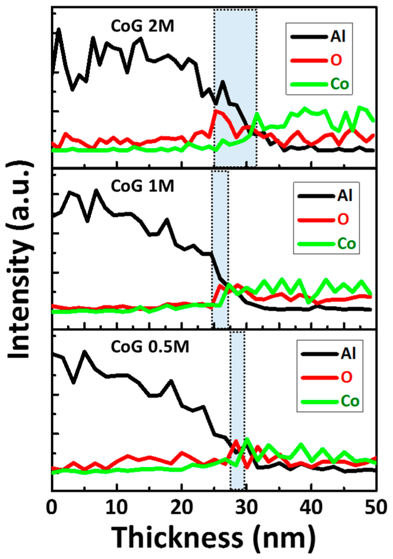
The thicknesses of native Al oxide were determined using TEM line-scan profiles. Figure 6 shows the TEM line-scan profiles of the CoG 0.5 M, 1 M, and 2 M memory devices. The native Al oxide layer measures around 5, 2, and ~1 nm for the CoG 2 M, 1 M, and 0.5 M memory devices, respectively.
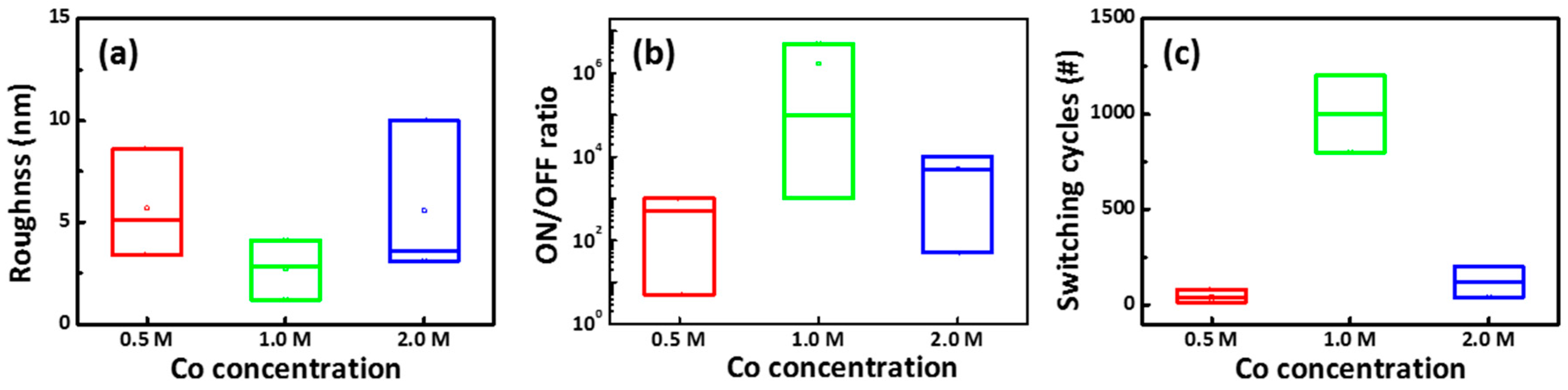
Figure 7a shows the relationship of the Rrms as a function of Co. concentration in the Al/CoG/ITO structure. The average Rrms values were counted by measuring six points in a 1.5 cm × 1.5 cm sample for each Co. concentration. As shown in Figure 7b,c, the statistical results for ON/OFF ratio and switching cycles of CoG 0.5, 1, and 2 M memory devices were randomly obtained from 20 out of 25 devices (80% in yield) in three fabricated substrates. Among these Co. concentrations, the smoothest surface, highest ON/OFF ratio, and best switching cycles occurred at 1 M Co. concentration. This result can be attributed to smooth roughness, which facilitates the stable resistive switching of the Resistive random-access memory (RRAM) device [14].
Figure 8a plots the scaling trend of the LRS current versus the cell area of the CoG 1 M memory device. The LRS current is mainly a filamentary conduction current, and the LRS only has a slight dependence on the cell area [15]. The independent LRS current with cell area confirms the filamentary nature of resistive switching in the CoG memory device. Temperature dependence of electrical transport can be used to gain insight into the nature of these conductive filaments. Figure 8b shows the temperature dependence of the LRS current in the CoG memory device. The thermally activated transport behavior excludes the possibility that the LRS comprises metallic filaments. CoG 1 M memory devices have improved endurance cycles. This property can be attributed to partial dissociation of conductive filaments in the CoG layer; by contrast, conductive filaments remain stable in the interfacial AlOx layer during subsequent switching cycles. The existence of the interfacial AlOx layer could considerably improve the device properties. The presence of the AlOx layer at the interface between CoG thin film and Al electrode correlates with the additional DC switching cycles observed in the Al/CoG 1 M/ITO cell. Intermediate oxide layers influenced their conduction behavior [16,17,18]. The suitable thickness of the interface AlOx layer acts as a diffusion barrier that prevents the infusion of oxygen into the atmosphere, similarly to an oxygen reservoir that stores and releases oxygen during switching.
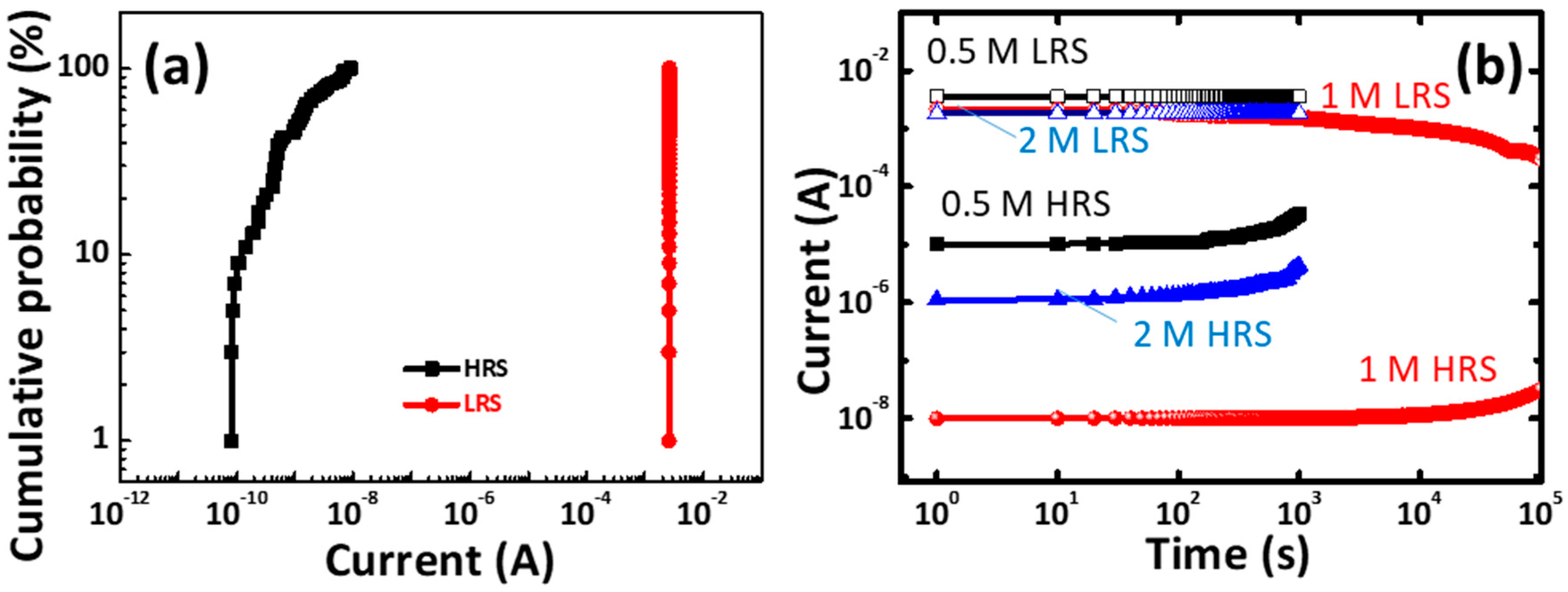
Figure 9a presents the statistical distribution parameters of the gelatin memory device The LRS and the HRS currents are measured at 0.1 V. Although the HRS was relatively broad, the LRS was well separated from the HRS, thereby allowing the two states to be distinguished. Figure 9b presents the retention capability of CoG 0.5, 1, and 2 M memory devices measured at room temperature and obtained at a voltage of 0.1 V. The ON/OFF ratio of the CoG memory device (1 M) remains higher than 105. The smooth roughness may facilitate stable resistive switching [19,20], and an improved retention capability is also achieved.
3. Materials and Methods
CoG thin films were fabricated on ITO/glass substrates by solution process. ITO/glass substrates (Aim Core Technology, Hsinchu, Taiwan) were cut to 2.0 cm × 1.5 cm and cleaned using acetone, methanol, and de-ionized (DI) water in an ultrasonic bath. Cobalt nitrate hexahydrate (Co.(NO3)2∙6H2O) and gelatin powder were added to DI water and stirred until the powders were completely dissolved. Then, the CoG solutions were spun on the cleaned ITO/glass substrates and baked at 80 °C for 10 min. The top electrode area of Al measured 3 mm2. The molar ratios of Co. and gelatin were fixed to 0.5:1, 1:1, and 2:1, and the Al/CoG 0.5 M/ITO, Al/CoG 1 M/ITO, and Al/CoG 2 M/ITO structures were fabricated.
Atomic force microscope (AFM) analysis (Dimension ICON with NanoScope V controller, Bruker, Billerica, MA, USA) was used to characterize the surface morphology and roughness of the obtained CoG/ITO samples. Scanning electron microscope (SEM) analysis was carried out using Hitachi SU8000 systems. The elements of the samples before measurement were mapped by EDX analysis (Bruker, Ettlingen, Germany). The electrical characteristics were measured by Agilent B1500 semiconductor characterization system (Agilent, Santa Clara, CA, USA).
4. Conclusions
In summary, a memory device based on simple solution-processed CoG thin film has been demonstrated. The uniform distribution of Co. in the CoG thin film can be observed by the EDX analyzer. The thicknesses of interfacial AlOx layer are suggested to increase with Co. concentration due to the assistance of the Co. redox reaction in the interfacial AlOx layer formation. The solution-processed Al/CoG 1 M/ITO structure exhibits excellent device performance, being forming-free, with a sufficient ON/OFF ratio of over 105 and extrapolated retention properties exceeding 10 years. In addition, increasing the Co. concentration up to 1 M increases the switching cycle, although it decreases when the Co. concentration reaches 2 M. The CoG 2 M memory device always fails at the LRS state, which means that the oxygen vacancies cannot obtain sufficient oxygen ions to rupture the filament paths. With Co. concentration of 1 M, the suitable thickness of the AlOx interface layer acts as an oxygen reservoir for storing and releasing oxygen during switching, which further improves the switching cycle endurance.
Acknowledgments
This work was supported in part by the National Science Council of Taiwan under Contracts NSC102-2221-E-006-182-MY3 and MOST 105-2221-E-006-193-MY3.
Author Contributions
Cheng-Jung Lee was responsible for device preparation and characterization, data analysis, and paper writing. Yu-Chi Chang was responsible for the modeling discussion and paper editing. Li-Wen Wang was also responsible for the material/device preparation and discussion. Yeong-Her Wang was an advisor in the monitoring of the progress of the paper, and in the editing.
Conflicts of Interest
The authors declare no conflict of interest.
References
- Chang, Y.C.; Wang, Y.H. Resistive switching behavior in gelatin thin films for nonvolatile memory application. ACS Appl. Mater. Interfaces 2014, 6, 5413–5421. [Google Scholar] [CrossRef] [PubMed]
- Ma, L.P.; Liu, J.; Yang, Y. Organic electrical bistable devices and rewritable memory cells. Appl. Phys. Lett. 2002, 80, 2997–2999. [Google Scholar] [CrossRef]
- Ma, L.P.; Pyo, S.M.; Ouyang, J.Y.; Xu, Q.F.; Yang, Y. Nonvolatile electrical bistability of organic/metal-nanocluster/organic system. Appl. Phys. Lett. 2003, 82, 1419–1421. [Google Scholar] [CrossRef]
- Busby, Y.; Monteiro, N.C.; Girleanu, M.; Brinkmann, M.; Ersen, O.; Pireaux, J.J. 3D imaging of filaments in organic resistive memory devices. Org. Electron. 2015, 16, 40–45. [Google Scholar] [CrossRef]
- Casula, G.; Cosseddu, P.; Busby, Y.; Pireaux, J.J.; Rosowski, M.; Szczesna, B.T.; Soliwoda, K.; Celichowski, G.; Grobelny, J.; Novák, J.; et al. Air-stable, non-volatile resistive memory based on hybrid organic/inorganic nanocomposites. Org. Electron. 2015, 18, 17–23. [Google Scholar] [CrossRef]
- Pollack, B.; Holmberg, S.; George, D.; Tran, I.; Madou, M.; Ghazinejad, M. Nitrogen-Rich Polyacrylonitrile-Based Graphitic Carbons for Hydrogen Peroxide Sensing. Sensors 2017, 17, 2047. [Google Scholar] [CrossRef] [PubMed]
- Ai, G.; Mo, R.; Li, H.; Zhong, J. Cobalt phosphate modified TiO2 nanowire arrays as co-catalysts for solar water splitting. Nanoscale 2015, 7, 6722–6728. [Google Scholar] [CrossRef] [PubMed]
- Andrew Lin, K.-Y.; Chen, Y.-C.; Huang, C.-F. Magnetic carbon-supported cobalt prepared from one-step carbonization of hexacyanocobaltate as an efficient and recyclable catalyst for activating Oxone. Sep. Purif. Technol. 2016, 170, 173–182. [Google Scholar] [CrossRef]
- Lampert, M.A. Simplified theory of space-charge-limited currents in an insulator with traps. Phys. Rev. 1956, 103, 1648. [Google Scholar] [CrossRef]
- Nishi, Y.; Suzuki, M.; Koyama, M. Bipolar resistive switch effects in calcium fluoride thin films deposited on silicon bottom electrodes. Appl. Phys. Express 2013, 6, 041202. [Google Scholar] [CrossRef]
- Waser, R.; Aono, M. Nanoionics-based resistive switching Memories. Nat. Mater. 2007, 6, 833–840. [Google Scholar] [CrossRef] [PubMed]
- Lv, H.; Wang, M.; Wan, H.; Song, Y.; Luo, W.; Zhou, P.; Tang, T.; Lin, Y.; Huang, R.; Song, S.; et al. Endurance enhancement of Cu-oxide based resistive switching memory with Al top electrode. Appl. Phys. Lett. 2009, 94, 213502. [Google Scholar] [CrossRef]
- Tungkavet, T.; Pattavarakorn, D.; Sirivat, A. Bio-compatible gelatins (Ala-Gly-Pro-Arg-Gly-Glu-4HypGly-Pro-) and electromechanical properties: Effects of temperature and electric field. J. Polym. Res. 2012, 19, 9759. [Google Scholar] [CrossRef]
- Hwang, Y.H.; An, H.M.; Cho, W.J. Performance improvement of the resistive memory properties of InGaZnO thin films by using microwave irradiation. Jpn. J. Appl. Phys. 2014, 53, 04EJ04. [Google Scholar] [CrossRef]
- Wong, H.S.P.; Lee, H.Y.; Yu, S.; Chen, Y.S.; Wu, Y.; Chen, P.S.; Lee, B.; Chen, F.T.; Tsai, M.J. Metal-oxide RRAM. Proc. IEEE 2012, 100, 1951–1970. [Google Scholar] [CrossRef]
- Do, Y.H.; Kwak, J.S.; Bae, Y.C.; Jung, K.; Im, H.; Hong, J.P. Oxygen ion drifted bipolar resistive switching behaviors in TiO2-Al electrode interfaces. Thin Solid Films 2010, 518, 4408–4411. [Google Scholar] [CrossRef]
- Shima, H.; Takano, F.; Muramatsu, H.; Akinaga, H.; Tamai, Y.; Inque, I.H.; Takagi, H. Voltage polarity dependent low-power and high-speed resistance switching in CoO resistance random access memory with Ta electrode. Appl. Phys. Lett. 2008, 93, 113504. [Google Scholar] [CrossRef]
- Wu, X.; Zhou, P.; Li, J.; Chen, L.Y.; Lv, H.B.; Lin, Y.Y.; Tang, T.A. Reproducible unipolar resistance switching in stoichiometric ZrO2 films. Appl. Phys. Lett. 2007, 90, 183507. [Google Scholar] [CrossRef]
- Chang, Y.C.; Lee, K.J.; Lee, C.J.; Wang, L.W.; Wang, Y.H. Bipolar resistive switching behavior in sol-gel MgTiNiOx memory device. IEEE J. Electron Devices Soc. 2016, 4, 321–327. [Google Scholar] [CrossRef]
- Visinoiu, A.; Scholz, R.; Alexe, M.; Hesse, D. Morphology dependence of the dielectric properties of epitaxial BaTiO3 films and epitaxial BaTiO3/SrTiO3 multilayers. Appl. Phys. A 2005, 80, 229–235. [Google Scholar] [CrossRef]
Figure 1.
X-ray photoelectron spectroscopy (XPS) survey spectra of cobalt embedded gelatin (CoG) (a) 0.5, (b) 1, and (c) 2 M thin films.
Figure 1.
X-ray photoelectron spectroscopy (XPS) survey spectra of cobalt embedded gelatin (CoG) (a) 0.5, (b) 1, and (c) 2 M thin films.
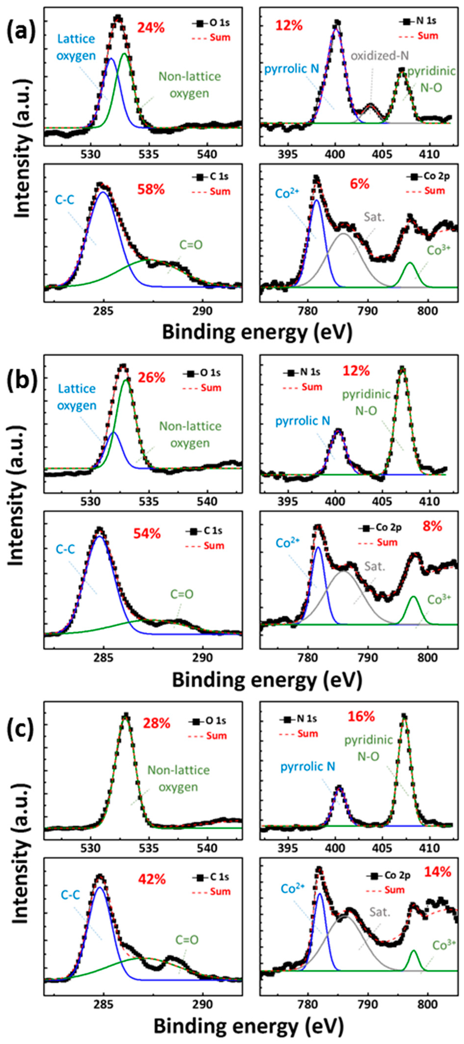
Figure 2.
Atomic force microscope (AFM) image of the CoG (a) 0.5, (b) 1, and (c) 2 M thin films. The height profiles shown are taken along the red lines.
Figure 2.
Atomic force microscope (AFM) image of the CoG (a) 0.5, (b) 1, and (c) 2 M thin films. The height profiles shown are taken along the red lines.

Figure 3.
(a) Typical I–V curves of the Al/CoG (concentrations of Co. = 0.5, 1, and 2 M)/ITO structures. (b) I–V fitting of the high-resistance state (HRS) and low-resistance state (LRS) for the Al/CoG/ITO structure.
Figure 3.
(a) Typical I–V curves of the Al/CoG (concentrations of Co. = 0.5, 1, and 2 M)/ITO structures. (b) I–V fitting of the high-resistance state (HRS) and low-resistance state (LRS) for the Al/CoG/ITO structure.

Figure 4.
TEM cross-sectional energy-dispersive X-ray spectroscopy (EDS) mapping of the CoG 1 M memory devices.
Figure 4.
TEM cross-sectional energy-dispersive X-ray spectroscopy (EDS) mapping of the CoG 1 M memory devices.
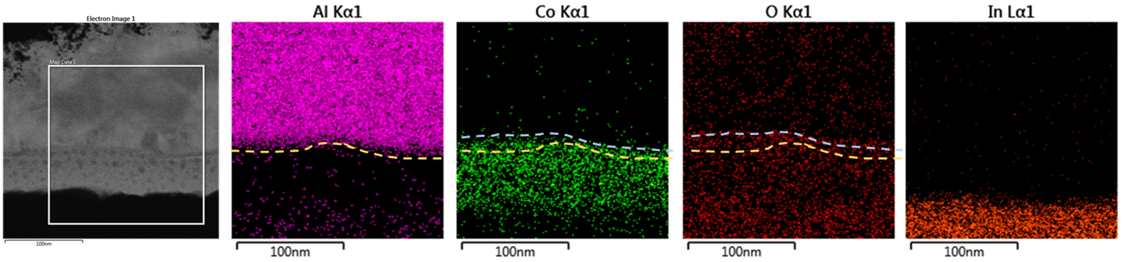
Figure 5.
Here, EDS C (red), N (blue), O (green), and Co. (orange) element mapping images of CoG (a) 0.5, (c) 1, and (e) 2 M thin films are shown. The switching cycles of (b) Al/CoG (0.5 M)/ITO, (d) Al/CoG (1 M)/ITO, and (f) Al/CoG (2 M)/ITO structures can also be seen. The inset of (d) shows the low-field I–V characteristics corresponding to a typical pristine state (LRS and HRS).
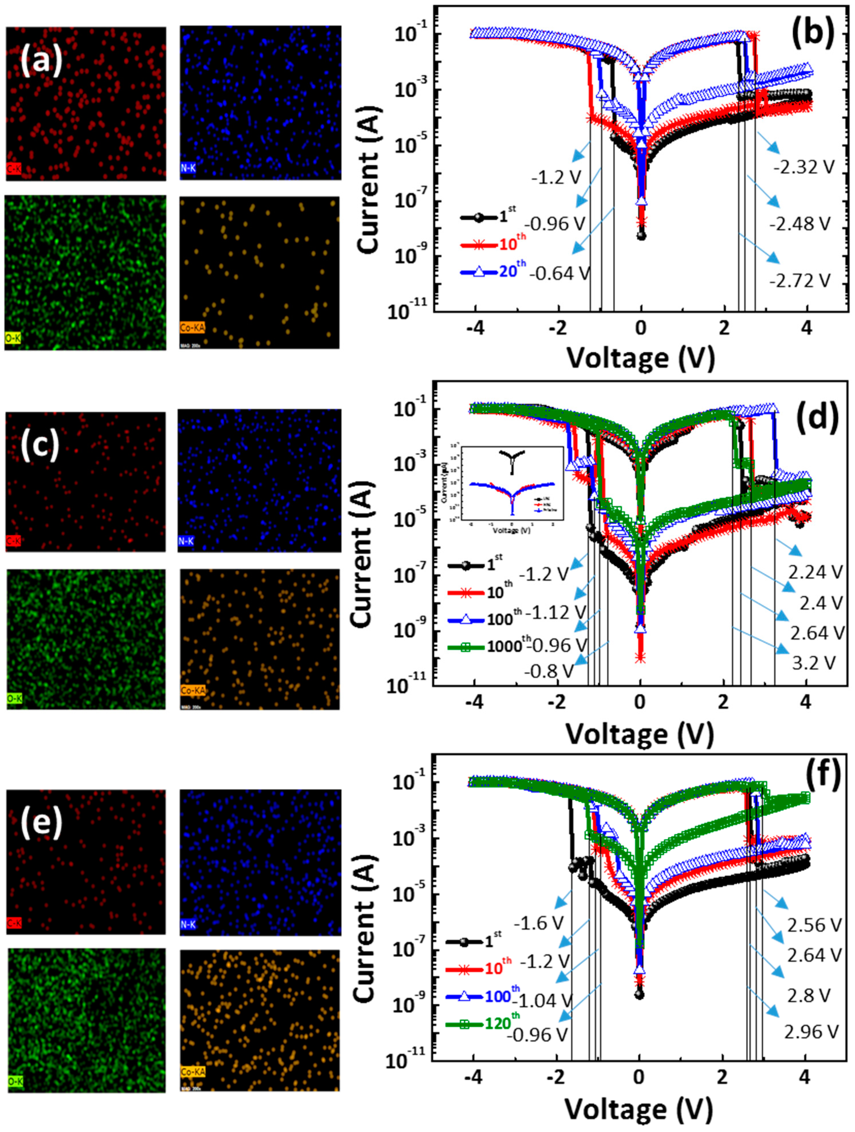
Figure 6.
TEM line-scan profiles of the CoG 0.5 M, 1 M, and 2 M memory devices.

Figure 7.
Relationship among the (a) Rrms; (b) ON/OFF ratio; (c) switching cycles, and Co. concentrations in the Al/CoG/ITO (read at 0.5 V).
Figure 7.
Relationship among the (a) Rrms; (b) ON/OFF ratio; (c) switching cycles, and Co. concentrations in the Al/CoG/ITO (read at 0.5 V).

Figure 8.
(a) LRS current versus cell area; and (b) electrical transport thermally activated for the set states of the CoG 1 M memory device.
Figure 8.
(a) LRS current versus cell area; and (b) electrical transport thermally activated for the set states of the CoG 1 M memory device.
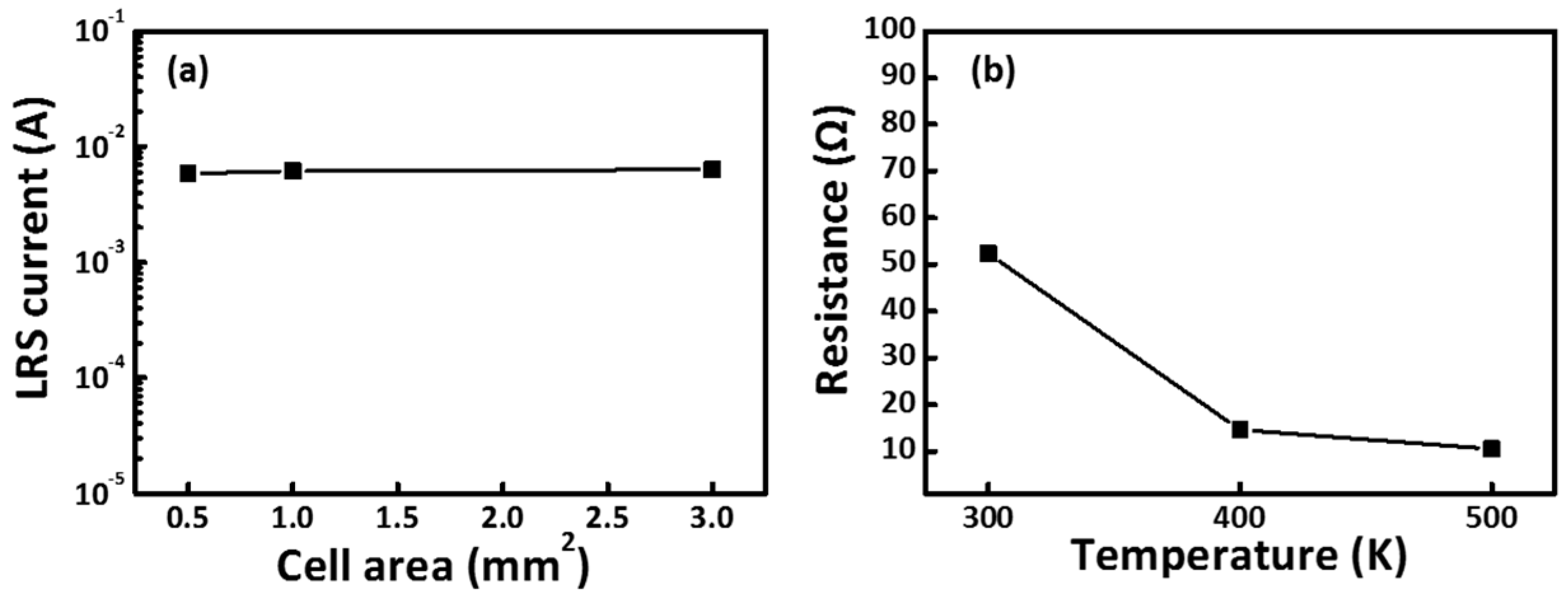
Figure 9.
(a) Statistical distributions of current values of Al/CoG (1 M)/ITO structure; (b) Retention characteristics of the CoG (0.5, 1, and 2 M) memory devices.
Figure 9.
(a) Statistical distributions of current values of Al/CoG (1 M)/ITO structure; (b) Retention characteristics of the CoG (0.5, 1, and 2 M) memory devices.

© 2017 by the authors. Licensee MDPI, Basel, Switzerland. This article is an open access article distributed under the terms and conditions of the Creative Commons Attribution (CC BY) license (http://creativecommons.org/licenses/by/4.0/).
Share and Cite
MDPI and ACS Style
Lee, C.-J.; Chang, Y.-C.; Wang, L.-W.; Wang, Y.-H. Nonvolatile Resistive Switching Memory Utilizing Cobalt Embedded in Gelatin. Materials 2018, 11, 32. https://doi.org/10.3390/ma11010032
AMA Style
Lee C-J, Chang Y-C, Wang L-W, Wang Y-H. Nonvolatile Resistive Switching Memory Utilizing Cobalt Embedded in Gelatin. Materials. 2018; 11(1):32. https://doi.org/10.3390/ma11010032
Chicago/Turabian StyleLee, Cheng-Jung, Yu-Chi Chang, Li-Wen Wang, and Yeong-Her Wang. 2018. "Nonvolatile Resistive Switching Memory Utilizing Cobalt Embedded in Gelatin" Materials 11, no. 1: 32. https://doi.org/10.3390/ma11010032
Note that from the first issue of 2016, this journal uses article numbers instead of page numbers. See further details here.