Perpendicular Magnetic Anisotropy in Heusler Alloy Films and Their Magnetoresistive Junctions


1
Department of Electronic Engineering, University of York, York YO10 5DD, UK
2
Department of Physics, University of York, York YO10 5DD, UK
*
Author to whom correspondence should be addressed.
Materials 2018, 11(1), 105; https://doi.org/10.3390/ma11010105
Submission received: 21 December 2017
/
Revised: 4 January 2018
/
Accepted: 5 January 2018
/
Published: 11 January 2018
(This article belongs to the Special Issue Magnetoresistance Effects and Their Application to Spintronic Devices)
Abstract
:For the sustainable development of spintronic devices, a half-metallic ferromagnetic film needs to be developed as a spin source with exhibiting 100% spin polarisation at its Fermi level at room temperature. One of the most promising candidates for such a film is a Heusler-alloy film, which has already been proven to achieve the half-metallicity in the bulk region of the film. The Heusler alloys have predominantly cubic crystalline structures with small magnetocrystalline anisotropy. In order to use these alloys in perpendicularly magnetised devices, which are advantageous over in-plane devices due to their scalability, lattice distortion is required by introducing atomic substitution and interfacial lattice mismatch. In this review, recent development in perpendicularly-magnetised Heusler-alloy films is overviewed and their magnetoresistive junctions are discussed. Especially, focus is given to binary Heusler alloys by replacing the second element in the ternary Heusler alloys with the third one, e.g., MnGa and MnGe, and to interfacially-induced anisotropy by attaching oxides and metals with different lattice constants to the Heusler alloys. These alloys can improve the performance of spintronic devices with higher recording capacity.
1. Introduction
Since the discovery of giant magnetoresistance (GMR) by Fert [1] and Grünberg [2] independently, magnetoresistive (MR) junctions have been used widely in many spintronic devices [3,4], e.g., a read head in a hard disk drive (HDDs) [5], and a cell in a magnetic random access memory (MRAM) [6]. The maximum GMR ratio achieved in a [Co (0.8)/Cu (0.83)]60 (thickness in nm) junction was reported to be 65% at 300 K [7]. Here, the MR ratio is determined by
where RP and RAP represent the resistance measured for parallel and antiparallel configurations of the ferromagnet magnetisations, respectively. In parallel, tunnelling magnetoresistance (TMR) [8] has been observed by utilising an oxide barrier instead of a non-magnetic spacer at room temperature (RT) [9,10], and have been improved its ratio very rapidly to 81% in a Co0.4Fe0.4B0.2 (3)/Al (0.6)-Ox/Co0.4Fe0.4B0.2 (2.5) (thickness in nm) junction at RT [11]. By replacing amorphous AlOx with epitaxial MgO [12,13] as theoretically predicated [14,15], 604% TMR ratio has been achieved in a Co0.2Fe0.6B0.2 (6)/MgO (2.1)/Co0.2Fe0.6B0.2 (4) (thickness in nm) junction at RT [16]. Such drastic increase in the TMR ratio has increased the areal density of HDD by almost four times over the last decade, for example [3].
MR ratio = ΔR/R = (RAP − RP)/RP,
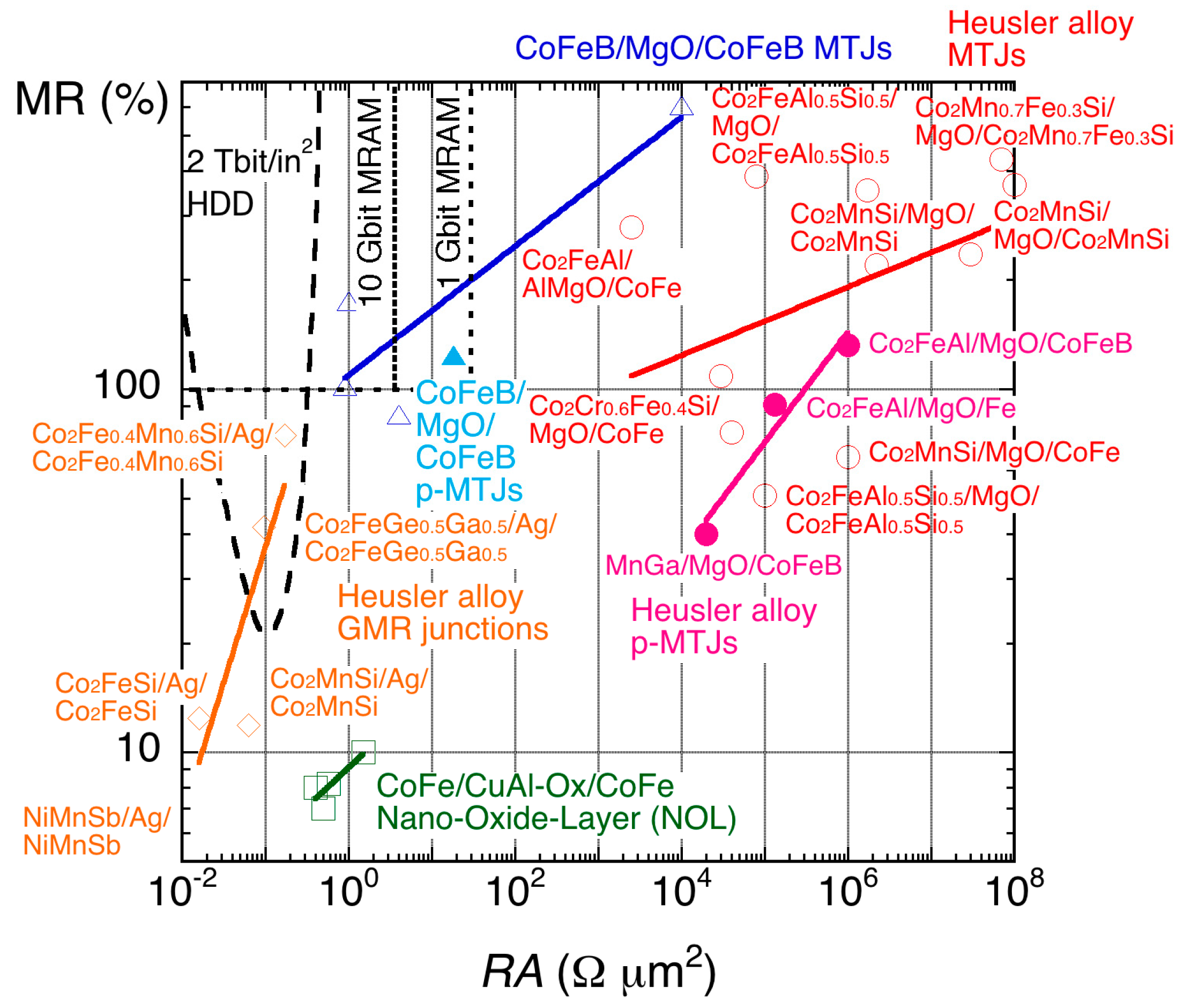
For further improvement in HDD and MRAM, it is critical to satisfy two criteria: (i) low resistance-area product (RA) and (ii) perpendicular magnetic anisotropy. The low RA is important to reduce power consumption and resulting unfavourable side effects, such as Joule heating and possible damage on spintronic devices. The perpendicular anisotropy is essential to achieve faster magnetisation switching [17,18] and to minimise stray fields from a MR junction and the associated cross-talk between the junction cells for MRAM. The recent development in MR ratios and RA is summarised in Figure 1. Figure 1 also includes the target requirements to achieve 1 Gbit MRAM, 10 Gbit MRAM and 2 Tbit/in2 HDD [19].
For the 1 Gbit MRAM, the junction cell diameter (fabrication rule) should be <65 nm with RA < 30 Ω·µm2 and MR ratio > 100% [19]. For the 10 Gbit MRAM, the cell diameter should be <20 nm with RA < 3.5 Ω·µm2 and MR ratio >100%. Here, low RA is required to satisfy the impedance matching [20] with a transistor attached to one MRAM cell and a large MR ratio is essential to maintain a signal-to-noise ratio allowing for a read-out signal voltage to be detected by a small-current application. In order to achieve these requirements, intensive research has been performed on the CoFeB/MgO/CoFeB junctions. As shown as open triangles with a blue fit in Figure 1, in-plane CoFeB/MgO/CoFeB magnetic tunnel junctions (MTJs) have successfully satisfied the requirement for the 10 Gbit MRAM by achieving RA = 0.9 Ω·µm2 and TMR = 102% at RT [21]. Later, a perpendicularly-magnetised MTJ (p-MTJ) also achieved the requirement for the 1 Gbit MRAM with RA = 18 Ω·µm2 and TMR = 124% at RT [22], which requires further improvement for the 10 Gbit MRAM target. Such MTJs will replace the current-generation 256 Mbit MRAM with perpendicular magnetic anisotropy produced by Everspin [23].
For the 2 Tbit/in2 HDD, on the other hand, the MTJs cannot be used as the requirement for RA is almost one order of magnitude smaller than that for the 10 Gbit MRAM [24]. One attempt is nano-oxide layers (NOL), which restrict the current paths perpendicular to the GMR stack by oxidising a part of the Cu or Al spacer layer [25]. In a Co0.5Fe0.5 (2.5)/Al-NOL/Co0.5Fe0.5 (2.5) junction, RA = 0.5~1.5 Ω·µm2 and MR = 7~10% at RT has been achieved. These values are below the requirement for the 2 Tbit/in2 HDD, and hence further improvement in GMR or TMR junctions are crucial.
2. Heusler-Alloy Junctions
For the further improvement in the MR junctions to meet the requirements for 10 Gbit MRAM and 2 Tbit/in2 HDD, a half-metallic ferromagnet needs to be developed to achieve 100% spin polarisation at the Fermi energy at RT, leading to an infinite MR ratio using Equation (1). The half-metallicity is induced by the formation of a bandgap only in one of the electron-spin bands. There have been five types of half-metallic ferromagnets theoretically proposed and experimentally demonstrated to date: (i) oxide compounds (e.g., rutile CrO2 [26] and spinel Fe3O4 [27]); (ii) perovskites (e.g., (La,Sr)MnO3 [28]); and, (iii) magnetic semiconductors, including Zinc-blende compounds (e.g., EuO and EuS [29], (Ga,Mn)As [30] and CrAs [31]) and (iv) Heusler alloys (e.g., NiMnSb [32]). Magnetic semiconductors have been reported to show 100% spin polarisation due to their Zeeman splitting in two spin bands. However, their Curie temperature is still below RT [33]. Low-temperature Andreev reflection measurements have confirmed that both rutile CrO2 and perovskite La0.7Sr0.3MnO3 compounds possess almost 100% spin polarisation [34], however, no experimental report has been proved the half-metallicity at RT. As the most promising candidate for the RT half-metallicity, a Heusler alloy has been studied extensively as detailed in the following sections [35,36,37].
2.1. Heusler Alloys
2.1.1. Crystalline Structures
Since the initial discovery of ferromagnetism in a ternary Cu2MnAl alloy, consisting of non-magnetic elements by Heusler in 1903 [38], the Heusler alloys have been studied for various applications, including magnetic refrigeration [39] and shape memory [40]. The Heulser alloys are categorised into two types: full- and half-Heusler alloys in the forms of X2YZ and XYZ, respectively, where X and Y are transition metals and Z is a semiconductor or non-magnet. Figure 2a shows a schematic crystalline structure of the full-Heusler alloy in the perfectly ordered L21-phase. By mixing Y and Z, the alloy forms the partially-mixed B2-phase, while further mixing among X, Y, and Z makes the fully-disordered A2-phase. By replacing a half of X atoms with Y-site atoms, Y atoms with Z-site atoms and Z atoms with X-site atoms, inverse Heusler alloys in the D03-phase can be formed. The removal of a half of the X atoms makes the half-Heusler alloys in the C1b-phase. Additionally, a part of the constituent atoms can be replaced with the other atoms, allowing for controlling their crystalline and magnetic properties, such as lattice constants, magnetic moments, and magnetic anisotropy.
Due to the above complicated crystalline structures for the Heusler alloys, they require very high temperature (typically >1000 K in the bulk form and >650 K in the thin-film form) for their crystallisation [41]. This prevents the Heusler alloys to be used in spintronic devices. Recently, layer-by-layer growth in the Heusler alloy (110) plane (see Figure 2b) has been reported to decrease the crystallisation energy, i.e., the annealing temperature, by over 50% [42]. A similar crystallisation process has been demonstrated at higher temperature to uniformly crystallise the Heusler-alloy films [43].
2.1.2. Magnetic Properties
The robustness of the half-metallicity depends on the size and definition of the bandgap formed in one electron-spin band in the vicinity of Fermi energy. The bandgap is formed by the strong d-band hybridisation between the two transition metals of X and Y, according to ab initio calculations [34]. Typically, the bandgap of 0.4~0.8 eV is expected to be formed at 0 K [36]. At a finite temperature, however, the bandgap becomes smaller and the edge definition of the gap becomes poorly-defined. The bandgap has been measured by detecting photon absorption of circularly-polarised infrared light with energy corresponding to the bandgap [44].
The other advantage of the Heusler alloys is their controllability of their magnetic properties, such as their saturation magnetisation and Curie temperature. The total spin moments per Heusler alloy formula unit (f.u.) (Mt) have been reported to follow the generalised Slater-Pauling curve as Mt = Zt − 24 (full-Heusler) and Mt = Zt − 18 (half-Heusler), where Zt is the total number of valence-band electrons (see Figure 3) [45]. The atomic substitutions of any constituent atoms in the Heusler alloys can continuously change their magnetic moments and allows for customising the alloys for a specific application. There are over 2500 combinations to form Heusler alloys [36], among which a few tens of alloys have been reported to become half-metallic ferromagnets according to theoretical calculations. The atomic substitution further increase the applicability of the alloys for custom design.
2.2. Heusler Alloy Junctions with In-Plane Magnetic Anisotropy
2.2.1. Tunnelling Magnetoresistive Junctions
(1) Co2(Cr,Fe)Z
A pioneering work on a Heusler-alloy junction has been carried out by Block et al. [46]. They have reported a large negative MR ratio at RT in a quarternary full-Heusler Co2Cr0.6Fe0.4Al alloy, which experimentally demonstrates the controllability of the magnetic properties of the alloys by substituting their constituent elements. They report 30% MR at RT with pressed powder compacts, which acts as a series of MTJs. The Co2(Cr,Fe)Al alloys have then been used in MTJs in their polycrystalline form. A MTJ with the structure of Co2Cr0.6Fe0.4Al/AlOx/CoFe shows 16% TMR at RT [47], which is later improved up to 19% at RT by the barrier optimisation [48].
Recently, an epitaxial L21-Co2Cr0.6Fe0.4Al film sputtered onto MgO(001) substrate has been adopted for a fully epitaxial MTJ, consisting of Co2Cr0.6Fe0.4Al/MgO/CoFe, showing 42% at RT (74% at 55 K) [49]. Even though this film possesses the crystalline relationship Co2Cr0.6Fe0.4Al(001)[100]||MgO(001)[110], the magnetic moment is estimated to be 3.3 µB/f.u., which is smaller than the calculation (3.7 µB/f.u.) [50]. This indicates that the film contains an atomically disordered phase, which is also suggested from the decrease in the TMR ratios that are measured below 55 K. Further optimisation results in the TMR ratio to become 109% at RT and 317% at 4 K with RA ~ 3 × 10⁴ Ω·µm2 [51].
The half-metallicity of the Co2Cr1-xFexAl full-Heusler alloys has been found to be robust against the atomic disorder using first-principles calculations by Shirai et al. [52]. In the Co2CrAl alloys, the atomic disorder between Cr and Al, which eventually deforms the crystalline structure from L21 into B2 at a disorder level of 0.5, maintains the very high spin polarisation (P) of 97% for L21 and 93% for B2. The Co-Cr type disorder, however, destroys the half-metallicity rapidly, i.e., P to zero at a disorder level of 0.4 and Mt to be 2.0 µB/f.u. at the full disorder. For the Fe substitution x with Cr, high P is calculated to be maintained above 90% up to x = 0.35. Similarly, the CrFe-Al type disorder preserves both spin polarisation and the magnetic moment to be above 80% and 3.7 µB/f.u., respectively, up to the disorder level of 0.5, while the Co-CrFe disorder eliminates P at the disorder level of 0.3. These findings may explain the decrease in the measured TMR ratios as compared with the theoretically predicted value due to the interfacial disorder.
Strain also affects the half-metallicity in the Co2CrAl alloy, according to calculations [53]. P stays 100% in the lattice strain range between 1 and +3%, and is even higher than 90% up to +10% strain. The bandgap is also maintained against the strain and can be maximised under +3% strain. P also remains 100% against the tetragonal distortion in the range of ±2%, which is a great advantage for the epitaxial growth study on a GaAs substrate [54] and the other seed layers.
Unlike Co2CrAl, Co2FeAl is not theoretically predicted to be half-metallic [50]. Even so, Epitaxial Co2FeAl films are grown on GaAs(001) with the relationship Co2FeAl(001)[110]||GaAs(001)[110]. Accordingly, an epitaxial full Heusler Co2FeAl film with the L21 structure is also applied for a MTJ but shows only 9% TMR at RT [54]. These small TMR ratios may be caused by the selective oxidation at the interface between the Heusler films and the oxide barriers. The TMR ratios have been increased to 330% at RT (700% at 10 K) with RA = 1 × 10³ Ω·µm2 in a MTJ with Co2FeAl/MgO/Co0.75Fe0.25 by utilising the Δ1-band connection between Co2FeAl and MgO [55]. Using a MgAlOx barrier instead of MgO to maintain the Δ1-band connection and to make better lattice matching with B2-Co2FeAl, TMR ratios are found to be increased to 342% at RT (616% at 4 K) with RA = 2.5 × 10³ Ω·µm2 [56]. The departure of the TMR ratios from theoretically predicted almost infinity may also be due to the interfacial atomic disorder, due to the presence of a light element of aluminium.
By replacing a half of Al with Si in Co2FeAl to stabilise the crystallisation, MTJs with an oriented MgO barrier for which TMR ratios of 175% have been achieved at RT when using B2-Co2FeAl0.5Si0.5 [57]. Using L21-Co2FeAl0.5Si0.5, the TMR ratios of 386% at RT and 832% at 9 K with RA = 80 × 103 Ω·µm2 has been reported later [58]. The decrease in the TMR ratio with increasing temperature is much faster than the temperature dependence of the magnetisation T3/2, suggesting that a small fraction of atomically disordered phases cannot be ignored in the spin-polarised electron transport at finite temperatures [59]. The elimination of such disordered interfacial phases improves the TMR ratios further and realises the half-metallicity at RT.
Theoretical calculations suggest that the interface states within the half-metallic bandgap formed at the half-metal/insulator interfaces prevent the highly spin-polarised electron transport [60]. This is because the tunneling rate is slower than the spin-flip rate, and therefore the interface states for the minority spins are effectively coupled to the metallic spin reservoir of the majority spin states. In order to avoid the spin-flip scattering, a sharp interface without the interface states is crucially required.
(2) Co2MnZ
Another pioneering work on the growth of full Heusler alloy films has been performed for a Co2MnGe/GaAs(001) hybrid structure by Ambrose et al. [61]. They achieve an epitaxial Co2MnGe film with a slightly enhanced lattice constant as compared with bulk. Mt is estimated to be 5.1 µB/f.u., which almost perfectly agrees with the bulk and theoretically predicted value from the generalised Slater-Pauling curve. Consequently, systematic study has been widely carried out over Co2Mn-based full Heusler alloys to realise the RT half-metallicity: Co2MnAl [62,63], Co2MnSi [64,65], Co2MnGa [66], and Co2MnSn [64]. For example, an epitaxial Co2MnAl film has been grown on a Cr buffer layer by sputtering with the crystalline relationship Co2MnAl(001)[110]||Cr(001)[110]||MgO(001)[100] with the B2 structure [60]. For Co2MnSi, the L21 structure has been deposited by using both dc magnetron sputtering [67] and MBE [68].
Calculations imply that the strain induced can control the half-metallicity in the Co2MnZ alloys. For Co2MnSi, for example, the lattice compression of 4% increases the bandgap by 23%, and a similar behavior is expected for the other alloy compounds [69]. Similarly, ±2% change in the lattice constant preserves the half-metallicity in the Co2MnZ alloys [33].
A MTJ with an epitaxial L21-Co2MnSi film has been reported to show very large TMR ratios of 70% at RT and 159% at 2 K with RA = 106 Ω·µm2 [70]. These values are the largest TMR ratios obtained in a MTJ employing a Heusler-alloy film and AlOx barrier. This is purely induced by the intrinsic P of the Heusler electrodes. Similarly, a MTJ with Co2MnAl/AlOx/CoFe shows 40% TMR at RT [63], followed by the further improvement up to 61% at RT (83% at 2 K) [71]. All of these Heusler films in the MTJs have been reported to be B2 structure. By comparing the TMR ratios at RT with those at low temperature, the TMR ratios are found to show very weak temperature dependence as similarly observed for a conventional metallic MTJ. On the contrary, a MTJ with a highly ordered Co2MnSi film shows strong temperature dependence; 33% at RT and 86% at 10 K [72], and 70% at RT and 159% at 2 K [70]. Such rapid decrease in the TMR ratio with an increasing temperature is similar to that observed in MTJs with Co2(Cr,Fe)Al.
By replacing AlOx with MgO, a fully epitaxial MTJ, consisting of Co2MnSi/MgO/Co2MnSi, has been reported to achieve much higher TMR ratios, 217% at RT (753% at 2 K) [73] and 236% at RT (1135% at 4 K), but with larger RA of 3 × 10⁷ Ω·µm2 [74]. Further improvements in the TMR ratio to be 354% at RT (1995% at 4 K) have been achieved in the same system [75], followed by 366% at RT (2110% at 4 K) with RA = 108 Ω·µm2 [76]. Partial substitution of Mn with Fe in these MTJs to form Co2Mn0.73Fe0.27Si, TMR ratios are increased to 429% at RT (2610% at 4 K) with RA = 7 × 10⁷ Ω·µm2 [77], which is the largest TMR ratio reported to date. A similar MTJ with Co2MnGe/MgO/Co2MnGe has been fabricated to show similar TMR ratios of 220% (650% at 4 K), but with large RA of 2.2 × 10⁶ Ω·µm2 [78].
(3) Ni2MnZ
Even though Ni2MnZ alloys are not predicted to become half-metallic ferromagnets by calculations, detailed studies on epitaxial growth on GaAs and InAs has been reported by Palmstrøm et al. [79]. By using a Sc0.3Er0.7As buffer layer on GaAs(001), both Ni2MnAl [80] and Ni2MnGa [81,82] films are epitaxially grown with the crystalline relation-ship Ni2MnGa(001)[100]||GaAs(001)[100] [83]. All the films are slightly tetragonally elongated along the plane normal as compared with the bulk values due to the minor lattice mismatch with the semiconductor substrates. First-principles calculations demonstrate that a broad energy minimum of tetragonal Ni2MnGa can explain stable pseudomorphic growth of Ni2MnGa on GaAs despite a nominal 3% lattice mismatch [84].
(4) Half-Heusler
After the first theoretical prediction of the half-metallicity of the half-Heusler NiMnSb alloy [30], this alloy has been intensively investigated to confirm its half-metallicity experimentally. Mt and the bandgap are calculated to be approximately 3.99 µB/f.u. and 0.5 eV [85], respectively, resulting in calculated spin polarisation of 99.3% [86]. Epitaxial NiMnSb(001) growth on GaAs(001) has also been studied systematically by van Roy et al. [87]. An epitaxial half Heusler NiMnSb film has been first used as an electrode in a MTJ, showing 9% TMR at RT [88].
2.2.2. Giant Magnetoresistive Junctions
Similar to the TMR junctions as discussed in Section 2.1.1, GMR junctions with Heusler-alloy films have been studied over the last decades. For example, a GMR junction, consisting of Co2MnGe (6)/V (1.6)/Co2MnGe (3)/Fe (0.3)/ZnSe (50)/GaAs(001) (thickness in nm) have been fabricated and measured along the two [110] directions [89]. The GMR ratio is measured to be less than 1%. Since then, a series of GMR juncstions have been designed and evaluated. An epitaxial film is deposited on a MgO(001) substrate with the crystalline relationship Co2Cr0.6Fe0.4Al(001)[100]||MgO(001)[110]. Here, by repeating [Co2Cr0.6Fe0.4Al (10)/Cu (2.5)/Fe0.1Co0.9 (8.1)] stack, current-in-the-plane (CIP) GMR has been measured, showing only 2% GMR at RT (4% at 15 K) [90]. Further enhancement has been reported in CPP-GMR devices, consisting of Co2FeAl0.5Si0.5 (2.5)/Ag (5)/Co2FeAl0.5Si0.5 (2.5) (thickness in nm), to be GMR ratios and RA of 34% and 8 × 10⁻³ Ω·μm2 at 290 K (80% at 14 K) [91].
Simultaneously, a large GMR ratio of 42% has been reported using Co2FeGe0.5Ga0.5/Ag/Co2FeGe0.5Ga0.5 junctions [92]. Theoretically, a larger GMR ratios are expected, e.g., 90% and ~60% for L21- and B2-Co2MnAl/Ag/Co2MnAl junctions, respectively [93]. These junctions clearly have the capability of being used as a next-generation read head.
Similar argument can be applied for the GMR junctions with the half-Heusler-alloy films. PtMnSb films are deposited on Al2O3(0001) by sputtering to form spin-valve structures, PtMnSb(111)/CuMnSb(111)/PtMnSb(111)/MnFe, showing 0.47% GMR at RT [94]. This may also be due to the empty site disorder. Calculations suggest the decrease in the surface spin polarisation dependent upon the terminated layers: spin polarisation of ~46% and 22% for the MnSb and Pt termination, respectively [95]. The other half Heusler alloy CoMnSb shows a similar decrease in the surface spin polarisation and the bandgap change by the strain: +2% and −2% lattice deformation shifts the bandgap by 0.8 eV and +0.9 eV, respectively [96]. Recently, current-perpendicular-to-the-plane (CPP)-GMR ratios of 8% at RT (21% at 4 K) has been reported in fully-epitaxial NiMnSb (20)/Ag (5)/NiMnSb (7) (thickness in nm) junctions with the (001) orientation [97]. The junctions achieve RA = (26 ± 1) × 10−3 Ω·μm2, which is highly advantageous for device applications with further improvement in the GMR ratios. By repeating two sets of epitaxial GMR junctions, consisting of NiMnSb (9)/Ag (5)/NiMnSb (3)/Ag (5)/NiMnSb (9) (thickness in nm), an increase in the CPP-GMR ratio up to 11% (41% at 4 K) has been reported later [98]. Here, RA is found to be reduced to 3.9 × 10⁻³ Ω·μm2, which is favourable for device application.
2.3. Heusler Alloy Junctions with Perpendicular Magnetic Anisotropy
2.3.1. Tunnelling Magnetoresistive Junctions
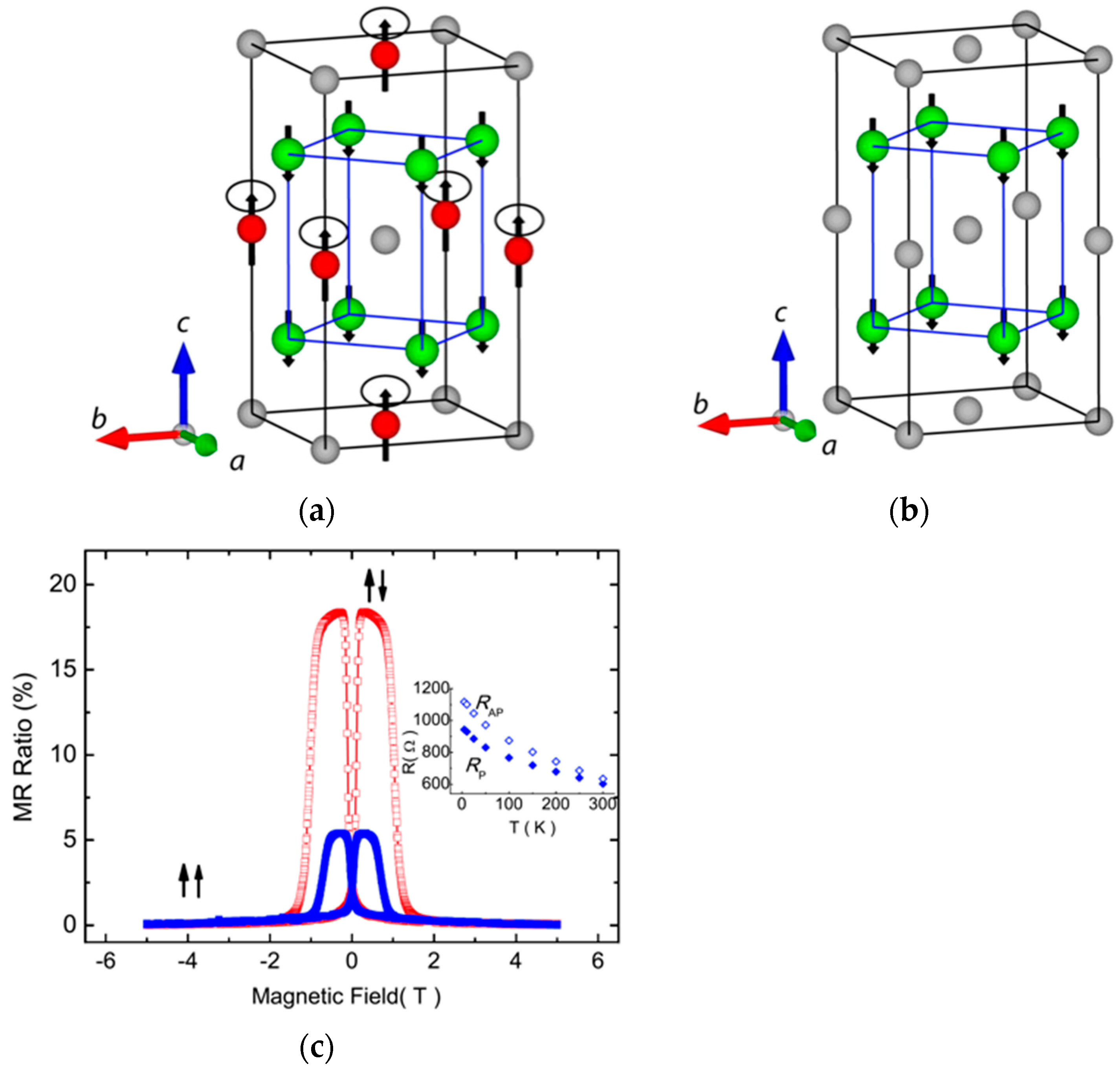
By replacing Y atoms with X atoms, binary Heusler alloys can be formed. For example, Mn3Ga shows ferrimagnetic behaviour in the tetragonal D022-phase with perpendicular magnetic anisotropy, as schematically shown in Figure 4a,b. The ferrimagnetic Mn3Ga has been reported to possess a large uniaxial anisotropy of 1 × 10⁷ erg/cm3 [99] and high Curie temperature of around 770 K [100]. Mn3Ga has been used in a MTJ, consisting of Mn3Ga/MgO/CoFe and has shown 9.8% TMR at 300 K with the perpendicular anisotropy of 1.2 × 10⁷ erg/cm3 [101]. The TMR ratio has then been improved by adjusting the Mn-Ga composition to be 40% at RT for the MTJ, consisting of Mn0.62Ga0.38 (30)/Mg (0.4)/MgO (1.8)/CoFeB (1.2) (thickness in nm) (see Figure 4c) [102]. This improvement may be due to the increase in the perpendicular anisotropy to be 5 × 10⁶ erg/cm3 in a similar MTJ [103], which is almost the same with that for the film reported above. However, the MTJ has 20 × 103 Ω·µm2, which requires further reduction for the spintronic device applications.
By inserting Co2MnSi between Mn-Ga and MgO, the perpendicular anisotropy of the Mn-Ga layer can induce perpendicular anisotropy in the half-metallic Co2MnSi layer, which is expected to achieve a large TMR ratio. Experimentally, TMR ratios of 10% at RT and 65% at 10 K have been achieved [105], which is smaller than the Mn-Ga/MgO/Mn-Ga junctions, as above. Additionally, the Co2MnSi magnetisation is in tilted states during the reversal process, which makes the TMR curves to be not well-defined.
Similar to the CoFeB/MgO/CoFeB systems, as described in Section 1, perpendicular anisotropy has been induced by attaching a MgO tunnel barrier. In a p-MTJ, consisting of Co2FeAl/MgO/Co0.2Fe0.6B0.2, a TMR ratio of 53% has been reported at RT (see Figure 5) [106]. By inserting a 0.1-nm-thick Fe (Co0.5Fe0.5) layer between the MgO and Co0.2Fe0.6B0.2 layers, the TMR ratio was significantly enhanced to 91% (82%), due to the improved interface. The corresponding RA is 1.31 × 10⁵ Ω·µm2. By further improving the MTJ quality, consisting of Co2FeAl (1.2)/MgO (1.8)/Fe (0.1)/CoFeB (1.3) (thickness in nm), it has been reported to show TMR = 132% and RA = 1 × 10⁶ Ω·µm2 at RT [107].
A perpendicularly magnetised seed layer has also been used to induce perpendicular anisotropy onto the Heusler-alloy films. For example, a MTJ stack with L10-CoPt/Co2MnSi/MgO/FePt has been demonstrated [108], as similarly reported in a conventional CoFeB/MgO/CoFeB junctions.
2.3.2. Giant Magnetoresistive Junctions
Recently, body-centred cubic (bcc) seed layers have been used to minimise the interfacial mixing with face-centred cubic (fcc) Heusler-alloy layer. For a bcc vanadium seed layer, X-ray analysis shows that 25-nm-thick vanadium introduces a strong (110) orientation in the Co2FeSi Heusler alloy [109]. The B2-texture of the Co2FeSi is found to match that of the vanadium proving that the texture is defined by the seed layer. Reduction of the Co2FeSi thickness is found to result in a reduction in the strength of the in-plane anisotropy, as expected from the cubic nature. Since the perpendicular magnetic anisotropy (PMA) is induced at the interface between the Co2FeSi and vanadium, a second vanadium interface is added and found to increase the observed PMA. Further reduction in the thickness of the Co2FeSi layer lead to an increase in the PMA where 4-nm-thick Co2FeSi exhibited a strong PMA (see Figure 6a). Here, the magnetic moment of the Co2FeSi layers all fell short of the bulk value with the saturation magnetisation (MS) of 700~800 emu/cm3. This may indicate magnetic dead layers at the interfaces due to roughness or intermixing; or could be due to a lack of full L21-ordering resulting in a drop in net moment.
Vanadium and tungsten are similar materials in that both are transition metal elements, which crystallise in a bcc structure. They have similar lattice parameters of aV = 0.3030 and aW = 0.31648 nm, leading to 3.3% and 17% strain in Co2FeSi, respectively. Tungsten is, however, of much lower bulk resistivity with a value of 5.6 × 10⁻⁶ Ω·cm [110], which is around half the value for vanadium to be 1.9 × 10⁻⁵ Ω·cm [111]. As such, tungsten should give similar if not superior results to vanadium as a seed layer.
Accordingly, tungsten layers of 10~20 nm are deposited under 5-nm-thick Co2FeSi, resulting in the (110) texture in Co2FeSi, as similarly observed for the V seed samples. However, the W seed layer is found to be heavily oxidised [112]. X-ray reflectivity (XRR) indicates a smooth film with low interfacial roughness of 0.4 nm for W/WOx/Co2FeSi, which is comparable with 0.5 nm for V/Co2FeSi. The sample with a 20 nm W/WOx seed layer exhibited clear in-plane anisotropy with a typical out-of-plane hard axis loop. The value of the anisotropy is low at only 1.58 × 10⁴ erg/cm3. This low value is due to the low value of MS of ~400 emu/cm3. The 10 nm thick W/WOx sample, however, exhibited a strong PMA in the Co2FeSi layer.
In an attempt to improve the quality of the tungsten seed layers, high temperature growth was utilised. The substrate is preheated to 673 K before deposition of 20 nm of tungsten. The resulting film shows a drastic reduction in oxidation with strongly crystallised tungsten. However, there is a lack of global texture as demonstrated by the multiple phases of tungsten. Scherrer analysis of the (110) peak gives an approximate crystallite size of 9 nm. The magnetisation of the W/Co2FeSi sample is measured to be 400 emu/cm3 with the perpendicular anisotropy of 8 × 10⁵ erg/cm3. These properties are summarised in Table 1.
3. Towards Device Implementation
Since the crystalline plane induced by the bcc seed layers is (110), which is a favourable orientation to promote the layer-by-layer crystallisation, low-temperature crystallisation has been demonstrated with PMA [115]. Samples consisting of W (10)/Co2FeAl0.5Si0.5 (12.5)/W (1.2)/Co2Fe Al0.5Si0.5 (2.5)/Ta (2) (thickness in nm) have been deposited with pre-growth heating at 300 ≤ T ≤ 370 K. Increasing temperature is found to cause a large increase in the crystallinity in the W(110) direction. As the heating time is increased, the position of the peak relaxed towards the bulk location, as shown in Figure 7a, corresponding a change in lattice spacing Δd = (0.0053 ± 0.0001) nm out-of-plane, i.e., a change in strain of Δs = (−2.4 ± 0.1) %. The position of the Heusler-alloy peak is not changed by increased deposition heating time. However, the intensity of the reflection increased significantly, indicating an increased crystallisation, as expected.
Magnetic characterisation of the samples is performed under both in- and out-of-the-plane fields. All of the samples with heated substrates showed perpendicular anisotropy. Figure 7b shows the coercivities (HC) and saturation magnetisations (MS) for the samples. HC and MS both increase monotonically with substrate temperature in agreement with the XRD data. The increased moment is due to the increase in the crystallisation of the material. After T = 305 K (30 s) the loop squareness decreases from MR/MS = 1, but remains high (>0.8) up to T = 370 K (120 s). MS reaches almost 1060 emu/cm3, which is almost 85% of the theoretically predicted value, and it is ideal for device implementation due to the low-temperature crystallisation.
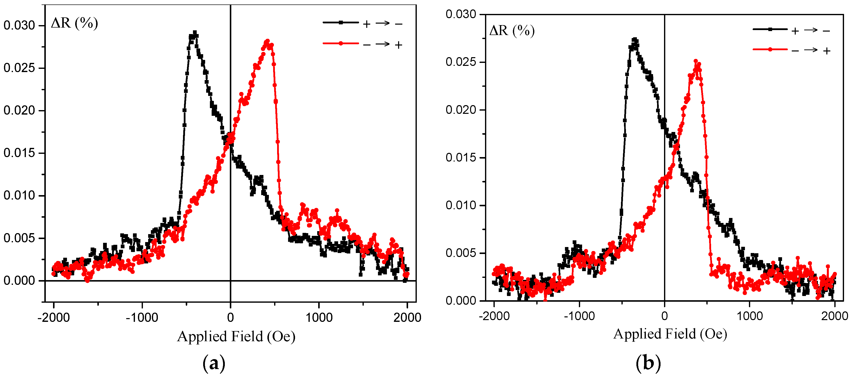
Due to band-structure matching silver makes an ideal conduction layer for Heusler alloy CPP-GMR devices. A 3 nm thick layer of Ag was deposited into a device structure Si sub./W (10)/Co2FeAl0.5Si0.5 (12.5)/Ag (3)/Co2FeAl0.5Si0.5 (5)/Ru (3) where thicknesses are in nm. These were patterned using e-beam lithography into elliptical devices with dimensions from (1000 × 500) nm2 to (150 × 100) nm2. The ΔR vs. field of these devices with a perpendicular applied field is shown in Figure 8 where a small but distinct GMR of 0.03% is observed at room temperature.
The shape of the MR curve matches that of the hysteresis loop for the sample, where domain rotation occurs to the antiparallel state, followed by a rapid nucleation reversal. This explains the asymmetry of the GMR peak, with a slow approach to a high resistance state, but a rapid return to the low resistance state at a definite field.
4. Materials and Methods
Epitaxial Heusler-alloy films have been deposited using ultrahigh vacuum (UHV) sputtering or molecular beam epitaxy (MBE) with precise control of compositions to satisfy their stoichiometry. For the UHV sputtering, compositions of targets need to be carefully optimised or combinatorial sputtering needs to be employed. For UHV MBE, simultaneous deposition is typically used on a single-crystal substrate. Polycrystalline Heusler-alloy films, on the other hand, have been grown by high-target utilisation sputtering system (HiTUS) [116]. In both of the films, substrate heating is often utilised to assist crystalline formation of the Heusler alloys. Here, the sputtering has higher energy on the materials to be deposited than those for UHV MBE by almost three orders of magnitude, allowing for the deposited films to be atomically well-mixed to form complex crystalline structures, as described in Section 2.1.1.
The deposited films have been characterised structurally and magnetically. The crystalline structures of the films are determined by X-ray diffraction (XRD, Rigaku, Tokyo, Japan) with chemical composition analysis, such as energy dispersive X-ray spectroscopy (EDX) and electron energy loss spectroscopy (EELS). Cross-sectional transmission electron microscopy (TEM, JEOL, Tokyo, Japan) is also used to investigate atomic ordering and interfacial structures of the films. The magnetisation loops of the films are measured using a vibrating sample magnetometer (VSM, MicroSense, Lowell, MA, USA) or similar methods under elevating temperatures. Temperature-dependent electrical resistivity measurements can also reveal the detailed scattering mechanism by defects in the films [52]. The half-metallicity can be determined by point-contact Andreev reflection (PCAR) [32] and infrared photoexcitation [42]. Additionally, X-ray magnetic circular dichroism (XMCD) with synchrotron radiation can reveal spin and orbital moments per constituent atoms [34].
The optimised Heusler-alloy films can be used as a ferromagnetic electrode in TMR and GMR junctions. The TMR junctions can be characterised using current-in-plane tunneling (CIPT) [117], which provides accurate TMR ratios. The GMR junctions can also be analysed by a conventional four-terminal method in a current-in-the-plane (CIP) configuration, which is more than one order of magnitude smaller than that in a CPP configuration. Therefore, these films are required to be patterned into nanometre-scale pillar junctions by electron beam lithography (EBL) and Ar-ion milling. The TMR or GMR junctions are patterned into nanopillars by EBL and Ar-ion milling, followed by the insulator deposition to isolate the pillars. For preparing the sample for electrical measurement, the top and the bottom of the pillar were connected to large contact pads via two-step lithography. Finally, smaller contacts were fabricated by EBL, and then the large contact pads were made by optical lithography.
5. Conclusions
The importance of the development of half-metallic ferromagnetic films for room-temperature operation has been increasing significantly. Among candidates for them, Heusler-alloy films have the greatest potential and have attracted intensive attention. Even though the bulk of the Heusler alloys have already been proven to be half-metallic, the film form still suffers from the interfacial atomic disorder against the neighbouring tunnelling barrier or non-magnetic spacer in magnetic tunnel or giant magnetoresistive junctions, respectively. For further improvement, the optimisation of growth conditions and the selection of better seed or barrier/spacer layers are crucial. Such improvement can also induce perpendicular magnetic anisotropy for the device miniaturisation. MgO- or bcc-seed-induced perpendicular anisotropy may lead to the Heusler-alloy films to satisfy the requirements for the next-generation spintronic devices.
Acknowledgments
William Frost and Atsufumi Hirohata acknowledge the financial support from Seagate Technologies in Northern Ireland. This study has been partially supported by Engineering and Physical Sciences Research Council (EPSRC) grant (EP/M02458X/1) in the United Kingdom.
Author Contributions
William Frost performed experiments and analyzed the data; Marjan Samiepour fabricated devices; Jun-young Kim contributed device characterization; Atsufumi Hirohata designed the experiments and analyzed the data; all the authors wrote the paper.
Conflicts of Interest
The authors declare no conflict of interest.
References
- Baibich, M.N.; Broto, J.M.; Fert, A.; Nguyen Van Dau, F.; Petroff, F.; Etienne, P.; Creuzet, G.; Friederich, A.; Chazelas, J. Giant magnetoresistance of (001)Fe/(001)Cr magnetic superlattices. Phys. Rev. Lett. 1988, 61, 2472–2475. [Google Scholar] [CrossRef] [PubMed]
- Binasch, G.; Grünberg, P.; Saurenbach, F.; Zinn, W. Enhanced magnetoresistance in layered magnetic structures with antiferromagnetic interlayer exchange. Phys. Rev. B 1989, 39, 4828(R)–4830(R). [Google Scholar] [CrossRef]
- Hirohata, A.; Takanashi, K. Future perspectives for spintronic devices. J. Phys. D Appl. Phys. 2014, 47, 193001. [Google Scholar] [CrossRef]
- Fullerton, E.E.; Schuller, I.K. The 2007 Nobel Prize in Physics: Magnetism and Transport at the Nanoscale. ACS Nano 2007, 1, 384–389. [Google Scholar] [CrossRef] [PubMed]
- Terris, B.D.; Thomson, T. Nanofabricated and self-assembled magnetic structures as data storage media. J. Phys. D Appl. Phys. 2005, 38, R199–R222. [Google Scholar] [CrossRef]
- Bhatti, S.; Sbiaa, R.; Hirohata, A.; Ohno, H.; Fukami, S.; Piramanayagam, S.N. Spintronics based random access memory: A review. Mater. Today 2017, 20, 530–548. [Google Scholar] [CrossRef]
- Parkin, S.S.P.; Li, Z.G.; Smith, D.J. Giant magnetoresistance in antiferromagnetic Co/Cu multilayers. Appl. Phys. Lett. 1991, 58, 2710–2712. [Google Scholar] [CrossRef]
- Jullière, M. Tunneling between ferromagnetic films. Phys. Lett. A 1975, 54, 225–226. [Google Scholar] [CrossRef]
- Miyazaki, T.; Tezuka, N. Giant magnetic tunneling effect in Fe/Al2O3/Fe junction. J. Magn. Magn. Mater. 1995, 139, L231–L234. [Google Scholar] [CrossRef]
- Moodera, J.S.; Kinder, L.R.; Wong, T.M.; Meservey, R. Large magnetoresistance at room temperature in ferromagnetic thin film tunnel junctions. Phys. Rev. Lett. 1995, 74, 3273–3276. [Google Scholar] [CrossRef] [PubMed]
- Wei, H.X.; Qin, Q.H.; Ma, M.; Sharif, R.; Han, X.F. 80% tunneling magnetoresistance at room temperature for thin Al–O barrier magnetic tunnel junction with CoFeB as free and reference layers. J. Appl. Phys. 2007, 101, 09B501. [Google Scholar] [CrossRef]
- Parkin, S.S.P.; Kaiser, C.; Panchkula, A.; Rice, P.M.; Hughes, B.; Samant, M.; Yang, S.-H. Giant tunnelling magnetoresistance at room temperature with MgO(100) tunnel barriers. Nat. Mater. 2004, 3, 862–867. [Google Scholar] [CrossRef] [PubMed]
- Yuasa, S.; Nagahama, T.; Fukushima, A.; Suzuki, Y.; Ando, K. Giant room-temperature magnetoresistance in single-crystal Fe/MgO/Fe magnetic tunnel junctions. Nat. Mater. 2004, 3, 868–871. [Google Scholar] [CrossRef] [PubMed]
- Butler, W.H.; Zhang, X.-G.; Schulthess, T.C.; MacLaren, J.M. Spin-dependent tunneling conductance of Fe|MgO|Fe sandwiches. Phys. Rev. B 2001, 63, 054416. [Google Scholar] [CrossRef]
- Mathon, J.; Umerski, A. Theory of tunneling magnetoresistance of an epitaxial Fe/MgO/Fe(001) junction. Phys. Rev. B 2001, 63, 220403(R). [Google Scholar] [CrossRef]
- Ikeda, S.; Hayakawa, J.; Ashizawa, Y.; Lee, Y.M.; Miura, K.; Hasegawa, H.; Tsunoda, M.; Matsukura, F.; Ohno, H. Tunnel magnetoresistance of 604% at 300 K by suppression of Ta diffusion in CoFeB/MgO/CoFeB pseudo-spin-valves annealed at high temperature. Appl. Phys. Lett. 2008, 93, 082508. [Google Scholar] [CrossRef]
- Rizal, C.; Fullerton, E.E. Perpendicular magnetic anisotropy and microstructure properties of nanoscale Co/Au multilayers. J. Phys. D Appl. Phys. 2017, 50, 355002. [Google Scholar] [CrossRef]
- Dieny, B.; Chshiev, M. Perpendicular magnetic anisotropy at transition metal/oxide interfaces and applications. Rev. Mod. Phys. 2017, 89, 025008. [Google Scholar] [CrossRef]
- Institute of Electrical and Electronics Engineers. Available online: http://www.ewh.ieee.org/r6/scv/mag/MtgSum/Meeting2012_05_Presentation.pdf (accessed on 20 August 2017).
- Schmidt, G.; Ferrand, D.; Molenkamp, L.W.; Filip, A.T.; van Wees, B.J. Fundamental obstacle for electrical spin injection from a ferromagnetic metal into a diffusive semiconductor. Phys. Rev. B 2000, 62, 4790(R)–4793(R). [Google Scholar] [CrossRef]
- Nagamine, Y.; Maehara, H.; Tsunekawa, K.; Djayaprawira, D.D.; Watanabe, N. Ultralow resistance-area product of 0.4 Ω(μm)2 and high magnetoresistance above 50% in CoFeB/MgO/CoFeB magnetic tunnel junctions. Appl. Phys. Lett. 2006, 89, 162507. [Google Scholar] [CrossRef]
- Ikeda, S.; Miura, K.; Yamamoto, H.; Mizunuma, K.; Gan, H.D.; Endo, M.; Kanai, S.; Hayakawa, J.; Matsukura, F.; Ohno, H. A perpendicular-anisotropy CoFeB–MgO magnetic tunnel junction. Nat. Mater. 2010, 9, 721–724. [Google Scholar] [CrossRef] [PubMed]
- Everspin. Available online: https://www.everspin.com/news/everspin-256mb-st-mram-perpendicular-mtj-sampling (accessed on 20 August 2017).
- Takagishi, M.; Yamada, K.; Iwasaki, H.; Fuke, H.N.; Hashimoto, S. Magnetoresistance ratio and resistance area design of CPP-MR film for 2–5 Tb/in2 read sensors. IEEE Trans. Magn. 2010, 46, 2086–2089. [Google Scholar] [CrossRef]
- Fuke, H.N.; Hashimoto, S.; Takagishi, M.; Iwasaki, H.; Kawasaki, S.; Miyake, K.; Sahashi, M. Magnetoresistance of FeCo nanocontacts with current-perpendicular-to-plane spin-valve structure. IEEE Trans. Magn. 2007, 43, 2848–2850. [Google Scholar] [CrossRef]
- Schwarz, K. CrO2 predicted as a half-metallic ferromagnet. J. Phys. F 1986, 16, L211–L215. [Google Scholar] [CrossRef]
- Yamase, A.; Shiratori, K. Band structure in the high temperature phase of Fe3O4. J. Phys. Soc. Jpn. 1984, 53, 312–317. [Google Scholar] [CrossRef]
- Okimoto, Y.; Katsufuji, T.; Ishikawa, T.; Urushibara, A.; Arima, T.; Tokura, Y. Anomalous variation of optical spectra with spin polarization in double-exchange ferromagnet: La1−xSrxMnO3. Phys. Rev. Lett. 1995, 75, 109–112. [Google Scholar] [CrossRef] [PubMed]
- Moodera, J.S.; Meservey, R.H. Spin-polarized tunneling. In Magnetoelectronics; Johnson, M., Ed.; Elsevier: Amsterdam, The Netherlands, 2004; pp. 163–204. ISBN 0-12-088487-9. [Google Scholar]
- Ohno, H. Ferromagnetic III–V semiconductors and their hetero-structures. In Semiconductor Spintronics and Quantum Computation; Awschalom, D.D., Loss, D., Samarth, N., Eds.; Springer: Berlin, Germany, 2002; pp. 1–30. ISBN 3-540-42176-9. [Google Scholar]
- Akinaga, H.; Manago, T.; Shirai, M. Material design of half-metallic Zinc-blende CrAs and the synthesis by molecular-beam epitaxy. Jpn. J. Appl. Phys. 2000, 39, L1118–L1120. [Google Scholar] [CrossRef]
- De Groot, R.A.; Mueller, F.M.; van Engen, P.G.; Buschow, K.H.J. New class of materials: Half-metallic ferromagnets. Phys. Rev. Lett. 1983, 50, 2024–2027. [Google Scholar] [CrossRef]
- Dietl, T.; Ohno, H.; Matsukura, F.; Cibert, J.; Ferrand, D. Zener model description of ferromagnetism in Zinc-Blende magnetic semiconductors. Science 2000, 287, 1019–1022. [Google Scholar] [CrossRef] [PubMed]
- Soulen, R.J., Jr.; Byers, J.M.; Osofsky, M.S.; Nadgorny, B.; Ambrose, T.; Cheng, S.F.; Broussard, C.T.; Tanaka, P.R.; Nowak, J.; Moodera, J.S.; et al. Measuring the spin polarization of a metal with a superconducting point contact. Science 1998, 282, 85–88. [Google Scholar] [CrossRef]
- Galanakis, I. Theory of Heusler and full-Heusler compounds. In Heusler Alloys; Felser, C., Hirohata, A., Eds.; Springer: Berlin, Germany, 2016; pp. 3–36. ISBN 978-3-319-21449-8. [Google Scholar]
- Hirohata, A.; Kikuchi, M.; Tezuka, N.; Inomata, K.; Claydon, J.S.; Xu, Y.B.; van der Laan, G. Heusler alloy/semiconductor hybrid structures. Curr. Opin. Solid State Mater. Sci. 2006, 10, 93–107. [Google Scholar] [CrossRef]
- Hirohata, A.; Sukegawa, H.; Yanagihara, H.; Žutić, I.; Seki, T.; Mizukami, S.; Swaminathan, R. Roadmap for emerging magnetic materials for spintronic device applications. IEEE Trans. Magn. 2015, 51, 0800511. [Google Scholar] [CrossRef]
- Heusler, F. Mangan-Aluminium-Kupferlegierungen. Verh. DPG 1903, 5, 219. [Google Scholar]
- Gutfleisch, O.; Gottschall, T.; Fries, M.; Benke, D.; Radulov, I.; Skokov, K.P.; Wende, H.; Gruner, M.; Acet, M.; Entel, P.; et al. Mastering hysteresis in magnetocaloric materials. Philos. Trans. R. Soc. A 2016, 85, 4358–4360. [Google Scholar] [CrossRef] [PubMed]
- Yu, G.-H.; Xu, Y.-L.; Liu, Z.-H.; Qiu, H.-M.; Zhu, Z.-Y.; Huang, X.-P.; Pan, L.-Q. Recent progress in Heusler-type magnetic shape memory alloys. Rare Met. 2015, 34, 527–539. [Google Scholar] [CrossRef]
- Hirohata, A.; Sagar, J.; Lari, L.; Fleet, L.R.; Lazarov, V.K. Heusler alloy films for spintronic devices. Appl. Phys. A 2013, 111, 423–430. [Google Scholar] [CrossRef]
- Sagar, J.; Fleet, L.R.; Walsh, M.; Lari, L.; Boyes, E.D.; Whear, O.; Huminiuc, T.; Vick, A.; Hirohata, A. Over 50% reduction in the formation energy of Co-based Heusler alloy films by two-dimensional crystallisation. Appl. Phys. Lett. 2014, 105, 032401. [Google Scholar] [CrossRef]
- Fleet, L.R.; Cheglakov, G.; Yoshida, K.; Lazarov, V.K.; Nakayama, T.; Hirohata, A. Layer-by-layer crystallization of Co2FeSi Heusler alloy thin films. J. Phys. D Appl. Phys. 2012, 45, 032001. [Google Scholar] [CrossRef]
- Alhuwaymel, T.F.; Abdullah, R.M.; Whear, O.; Huminiuc, T.; Carpenter, R.; El-Gomati, M.; Hirohata, A. New bandgap measurement technique for a half-metallic ferromagnet. IEEE Trans. Magn. 2014, 50, 2600504. [Google Scholar] [CrossRef]
- Skaftouros, S.; Özdoğan, K.; Şaşoğlu, E.; Galanais, I. Generalized Slater-Pauling rule for the inverse Heusler compounds. Phys. Rev. B 2013, 87, 024420. [Google Scholar] [CrossRef]
- Block, T.; Felser, C.; Jakob, G.; Ensling, J.; Mühling, B.; Gütlich, P.; Cava, R.J. Large negative magnetoresistance effects in Co2Cr0.6Fe0.4Al. J. Solid State Chem. 2003, 176, 646–651. [Google Scholar] [CrossRef]
- Inomata, K.; Okamura, S.; Goto, R.; Tezuka, N. Large tunneling magnetoresistance at room temperature using a Heusler alloy with the B2 structure. Jpn. J. Appl. Phys. 2004, 42, L419–L422. [Google Scholar] [CrossRef]
- Okamura, S.; Goto, R.; Sugimoto, S.; Tezuka, N.; Inomata, K. Structural, magnetic, and transport properties of full-Heusler alloy Co2(Cr1−xFex)Al thin films. J. Appl. Phys. 2004, 96, 6561–6564. [Google Scholar] [CrossRef]
- Marukame, T.; Kasahara, T.; Matsuda, K.-I.; Uemura, T.; Yamamoto, M. High tunnel magnetoresistance in epitaxial Co2Cr0.6Fe0.4Al/MgO/CoFe tunnel junctions. IEEE Trans. Magn. 2005, 41, 2603–2605. [Google Scholar] [CrossRef]
- Miura, Y.; Shirai, M.; Nagao, K. First-principles study on half-metallicity of disordered Co2(Cr1−xFex)Al. J. Appl. Phys. 2004, 95, 7225–7227. [Google Scholar] [CrossRef]
- Marukame, T.; Yamamoto, M. Tunnel magnetoresistance in fully epitaxial magnetic tunnel junctions with a full-Heusler alloy thin film of Co2Cr0.6Fe0.4Al and a MgO tunnel barrier. J. Appl. Phys. 2007, 101, 083906. [Google Scholar] [CrossRef]
- Miura, Y.; Nagao, K.; Shirai, M. Atomic disorder effects on half-metallicity of the full-Heusler alloys Co2(Cr1-xFex)Al: A first-principles study. Phys. Rev. B 2004, 69, 144413. [Google Scholar] [CrossRef]
- Block, T.; Carey, M.J.; Gurney, B.A.; Jepsen, O. Band-structure calculations of the half-metallic ferromagnetism and structural stability of full- and half-Heusler phases. Phys. Rev. B 2004, 70, 205114. [Google Scholar] [CrossRef]
- Hirohata, A.; Kurebayashi, H.; Okamura, S.; Kikuchi, M.; Masaki, T.; Nozaki, T.; Tezuka, N.; Inomata, K. Structural and magnetic properties of epitaxial L21-structured Co2(Cr,Fe)Al films grown on GaAs(001) substrates. J. Appl. Phys. 2005, 97, 103714. [Google Scholar] [CrossRef]
- Wang, W.; Sukegawa, H.; Shan, R.; Mitani, S.; Inomata, K. Giant tunneling magnetoresistance up to 330% at room temperature in sputter deposited Co2FeAl/MgO/CoFe magnetic tunnel junctions. Appl. Phys. Lett. 2009, 95, 182502. [Google Scholar] [CrossRef]
- Scheike, T.; Sukegawa, H.; Inomata, K.; Ohkubo, T.; Hono, K.; Mitani, S. Chemical ordering and large tunnel magnetoresistance in Co2FeAl/MgAl2O4/Co2FeAl(001) junctions. Appl. Phys. Exp. 2016, 9, 053004. [Google Scholar] [CrossRef]
- Tezuka, N.; Ikeda, N.; Sugimoto, S.; Inomata, K. 175% tunnel magnetoresistance at room temperature and high thermal stability using Co2FeAl0.5Si0.5 full-Heusler alloy electrodes. Appl. Phys. Lett. 2006, 89, 252508. [Google Scholar] [CrossRef]
- Tezuka, N.; Ikeda, N.; Mitsuhashi, F.; Sugimoto, S. Improved tunnel magnetoresistance of magnetic tunnel junctions with Heusler Co2FeAl0.5Si0.5 electrodes fabricated by molecular beam epitaxy. Appl. Phys. Lett. 2009, 94, 162504. [Google Scholar] [CrossRef]
- Hirohata, A.; Otani, Y. Heusler alloys: Experimental approach towards room-temperature half-metallicity. In Epitaxial Ferromagnetic Films and Spintronic Applications; Hirohata, A., Otani, Y., Eds.; Research Signpost: Kerala, India, 2009; pp. 224–225. ISBN 978-81-308-0319-7. [Google Scholar]
- Mavropoulos, P.; Ležaić, M.; Blügel, S. Half-metallic ferromagnets for magnetic tunnel junctions by ab initio calculations. Phys. Rev. B 2005, 72, 174428. [Google Scholar] [CrossRef]
- Ambrose, T.; Krebs, J.J.; Prinz, G.A. Epitaxial growth and magnetic properties of single-crystal Co2MnGe Heusler alloy films on GaAs(001). Appl. Phys. Lett. 2000, 76, 3280. [Google Scholar] [CrossRef]
- Kubota, H.; Nakata, J.; Oogane, M.; Ando, Y.; Sakuma, A.; Miyazaki, T. Large magnetoresistance in magnetic tunnel junctions using Co-Mn-Al full Heusler alloy. Jpn. J. Appl. Phys. 2004, 43, L984–L986. [Google Scholar] [CrossRef]
- Sakuraba, Y.; Nakata, J.; Oogane, M.; Kubota, H.; Ando, Y.; Sakuma, A.; Miyazaki, T. Fabrication of Co2MnAl Heusler alloy epitaxial film using Cr buffer layer. Jpn. J. Appl. Phys. 2005, 44, 6535–6537. [Google Scholar] [CrossRef]
- Geiersbach, U.; Bergmann, A.; Westerholt, K. Structural, magnetic and magnetotransport properties of thin films of the Heusler alloys Cu2MnAl, Co2MnSi, Co2MnGe and Co2MnSn. J. Magn. Magn. Mater. 2002, 240, 546–549. [Google Scholar] [CrossRef]
- Hashimoto, M.; Herfort, J.; Schönherr, H.-P.; Ploog, K.H. Epitaxial Heusler alloy Co2FeSi/GaAs(001) hybrid structures. Appl. Phys. Lett. 2005, 87, 102506. [Google Scholar] [CrossRef]
- Holmes, S.N.; Pepper, M. Magnetic and electrical properties of Co2MnGa grown on GaAs(001). Appl. Phys. Lett. 2002, 81, 1651–1653. [Google Scholar] [CrossRef]
- Singh, L.J.; Barber, Z.H.; Miyoshi, Y.; Branford, W.R.; Cohen, L.F. Structural and transport studies of stoichiometric and off-stoichiometric thin films of the full Heusler alloy Co2MnSi. J. Appl. Phys. 2004, 95, 7231–7233. [Google Scholar] [CrossRef]
- Wang, W.H.; Przybylski, M.; Kuch, W.; Chelaru, L.I.; Wang, J.; Lu, Y.F.; Barthel, J.; Meyerheim, H.L.; Kirschner, J. Magnetic properties and spin polarization of Co2MnSi Heusler alloy thin films epitaxially grown on GaAs(001). J. Phys. Rev. B 2005, 71, 144416. [Google Scholar] [CrossRef]
- Picozzi, S.; Continenza, A.; Freeman, A.J. Co2MnX (X = Si, Ge, Sn) Heusler compounds: An ab initio study of their structural, electronic, and magnetic properties at zero and elevated pressure. Phys. Rev. B 2002, 66, 094421. [Google Scholar] [CrossRef]
- Sakuraba, Y.; Nakata, J.; Oogane, M.; Kubota, H.; Ando, Y.; Sakuma, A.; Miyazaki, T. Huge Spin-polarization of L21-ordered Co2MnSi epitaxial Heusler alloy film. Jpn. J. Appl. Phys. 2005, 44, L1100–L1102. [Google Scholar] [CrossRef]
- Sakuraba, Y.; Nakata, J.; Oogane, M.; Ando, Y.; Kato, H.; Sakuma, A.; Miyazaki, T. Magnetic tunnel junctions using B2-ordered Co2MnAl Heusler alloy epitaxial electrode. Appl. Phys. Lett. 2006, 88, 022503. [Google Scholar] [CrossRef]
- Kämmerer, S.; Thomas, A.; Hütten, A.; Reiss, G. Co2MnSi Heusler alloy as magnetic electrodes in magnetic tunnel junctions. Appl. Phys. Lett. 2004, 85, 79–81. [Google Scholar] [CrossRef]
- Tsunegi, S.; Sakuraba, Y.; Oogane, M.; Takanashi, K.; Ando, Y. Large tunnel magnetoresistance in magnetic tunnel junctions using a Co2MnSi Heusler alloy electrode and a MgO barrier. Appl. Phys. Lett. 2008, 93, 112506. [Google Scholar] [CrossRef]
- Ishikawa, T.; Liu, H.; Taira, T.; Matsuda, K.; Uemura, T.; Yamamoto, M. Influence of film composition in Co2MnSi electrodes on tunnel magnetoresistance characteristics of Co2MnSi/MgO/Co2MnSi magnetic tunnel junctions. Appl. Phys. Lett. 2009, 95, 232512. [Google Scholar] [CrossRef]
- Liu, H.; Honda, Y.; Taira, T.; Matsuda, K.; Arita, M.; Uemura, T.; Yamamoto, M. Giant tunneling magnetoresistance in epitaxial Co2MnSi/MgO/Co2MnSi magnetic tunnel junctions by half-metallicity of Co2MnSi and coherent tunnelling. Appl. Phys. Lett. 2012, 101, 132418. [Google Scholar] [CrossRef]
- Hu, B.; Moges, K.; Honda, Y.; Liu, H.; Uemura, T.; Yamamoto, M.; Inoue, J.; Shirai, M. Temperature dependence of spin-dependent tunneling conductance of magnetic tunnel junctions with half-metallic Co2MnSi electrodes. Phys. Rev. B 2012, 94, 094428. [Google Scholar] [CrossRef]
- Liu, H.; Kawami, T.; Moges, K.; Uemura, T.; Yamamoto, M.; Shi, F.; Voyles, P.M. Influence of film composition in quaternary Heusler alloy Co2(Mn,Fe)Si thin films on tunnelling magnetoresistance of Co2(Mn,Fe)Si/MgO-based magnetic tunnel junctions. J. Phys. D Appl. Phys. 2015, 48, 164001. [Google Scholar] [CrossRef]
- Yamamoto, M.; Ishikawa, T.; Taira, T.; Li, G.; Matsuda, K.; Uemura, T. Effect of defects in Heusler alloy thin films on spin-dependent tunnelling characteristics of Co2MnSi/MgO/Co2MnSi and Co2MnGe/MgO/Co2MnGe magnetic tunnel junctions. J. Phys. Condens. Matter 2010, 22, 164212. [Google Scholar] [CrossRef] [PubMed]
- Palmstrøm, C. Epitaxial Heusler alloys: New materials for semiconductor spintronics. MRS Bull. 2003, 28, 725–728. [Google Scholar] [CrossRef]
- Dong, X.Y.; Dong, J.W.; Xie, J.Q.; Shih, T.C.; McKernan, S.; Leighton, C.; Palmstrøm, C. Growth temperature controlled magnetism in molecular beam epitaxially grown Ni2MnAl Heusler alloy. J. Cryst. Growth 2003, 254, 384–389. [Google Scholar] [CrossRef]
- Dong, J.W.; Chen, L.C.; Palmstrøm, C.J.; James, R.D.; McKernan, S. Molecular beam epitaxy growth of ferromagnetic single crystal (001) Ni2MnGa on (001) GaAs. Appl. Phys. Lett. 1999, 75, 1443–1445. [Google Scholar] [CrossRef]
- Dong, J.W.; Lu, J.; Xie, J.Q.; Chen, L.C.; James, R.D.; McKernan, S.; Palmstrøm, C.J. MBE growth of ferromagnetic single crystal Heusler alloys on (001)Ga1−xInxAs. Physica E 2001, 10, 428–432. [Google Scholar] [CrossRef]
- Dong, J.W.; Chen, L.C.; Xie, J.Q.; Müller, T.A.R.; Carr, D.M.; Palmstrøm, C.J. Epitaxial growth of ferromagnetic Ni2MnGa on GaAs(001) using NiGa interlayers. J. Appl. Phys. 2000, 88, 7357–7359. [Google Scholar] [CrossRef]
- Godlevsky, V.V.; Rabe, K.M. Soft tetragonal distortions in ferromagnetic Ni2MnGa and related materials from first principles. Phys. Rev. B 2001, 63, 134407. [Google Scholar] [CrossRef]
- Galanakis, I.; Mavropoulos, P.; Dederichs, P.H. Electronic structure and Slater-Pauling behaviour in half-metallic Heusler alloys calculated from first principles. J. Phys. D Appl. Phys. 2006, 39, 765–775. [Google Scholar] [CrossRef]
- Mavropoulos, P.; Galanakis, I.; Popescu, V.; Dederichs, P.H. The influence of spin-orbit coupling on the band gap of Heusler alloys. J. Phys. Condens. Matter 2004, 16, S5759–S5762. [Google Scholar] [CrossRef]
- Van Roy, W.; de Boeck, J.; Brijs, B.; Borghs, G. Epitaxial NiMnSb films on GaAs(001). Appl. Phys. Lett. 2000, 77, 4190–4192. [Google Scholar] [CrossRef]
- Tanaka, C.T.; Nowak, J.; Moodera, J.S. Magnetoresistance in ferromagnet-insulator-ferromagnet tunnel junctions with half-metallic ferromagnet NiMnSb compound. J. Appl. Phys. 1997, 86, 5515–5517. [Google Scholar] [CrossRef]
- Ambrose, T.; Krebs, J.J.; Prinz, G.A. Magnetotransport properties of single crystal Co2MnGe/NM/Co2MnGe trilayers epitaxially grown on GaAs (001). J. Appl. Phys. 2001, 89, 7522–7524. [Google Scholar] [CrossRef]
- Kelekar, R.; Clemens, B.M. Epitaxial growth of the Heusler alloy Co2Cr1−xFexAl. J. Appl. Phys. 2004, 96, 540–543. [Google Scholar] [CrossRef]
- Nakatani, T.M.; Furubayashi, T.; Kasai, S.; Sukegawa, H.; Takahashi, Y.K.; Mitani, S.; Hono, K. Bulk and interfacial scatterings in current-perpendicular-to-plane giant magnetoresistance with Co2FeAl0.5Si0.5 Heusler alloy layers and Ag spacer. Appl. Phys. Lett. 2010, 96, 212501. [Google Scholar] [CrossRef]
- Takahashi, Y.K.; Srinivasan, A.; Varaprasad, B.; Rajanikanth, A.; Hase, N.; Nakatani, T.M.; Kasai, S.; Furubayashi, T.; Hono, K. Large magnetoresistance in current-perpendicular-to-plane pseudospin valve using a Co2Fe(Ge0.5Ga0.5) Heusler alloy. Appl. Phys. Lett. 2011, 98, 152501. [Google Scholar] [CrossRef]
- Li, Y.; Xia, J.; Wang, G.; Yuan, H.; Chen, H. High-performance giant-magnetoresistance junction with B2-disordered Heusler alloy based Co2MnAl/Ag/Co2MnAl trilayer. J. Appl. Phys. 2015, 118, 053902. [Google Scholar] [CrossRef]
- Johnson, P.R.; Kautzky, M.C.; Mancoff, F.B.; Kondo, R.; Clemens, B.M.; White, R.L. Observation of giant magnetoresistance in a Heusler alloy spin valve. IEEE Trans. Magn. 1996, 32, 4615–4617. [Google Scholar] [CrossRef]
- Galanakis, I. Surface properties of the half-and full-Heusler alloys. J. Phys. Condens. Matter 2002, 14, 6329–6340. [Google Scholar] [CrossRef]
- Van Engen, P.G.; Buschow, K.H.J.; Jongebreur, R. PtMnSb, a material with very high magneto-optical Kerr effect. Appl. Phys. Lett. 1983, 42, 202–204. [Google Scholar] [CrossRef]
- Wen, Z.; Kubota, T.; Yamamoto, T.; Takanashi, K. Fully epitaxial C1b-type NiMnSb half-Heusler alloy films for current-perpendicular-to-plane giant magnetoresistance devices with a Ag spacer. Sci. Rep. 2015, 5, 18387. [Google Scholar] [CrossRef] [PubMed]
- Wen, Z.; Kubota, T.; Yamamoto, T.; Takanashi, K. Enhanced current-perpendicular-to-plane giant magnetoresistance effect in half-metallic NiMnSb based nanojunctions with multiple Ag spacers. Appl. Phys. Lett. 2016, 108, 232406. [Google Scholar] [CrossRef]
- Bang, H.-W.; Yoo, W.; Choi, Y.; You, C.-Y.; Hong, J.-I.; Dolinšek, J.; Jung, M.-H. Perpendicular magnetic anisotropy properties of tetragonal Mn3Ga films under various deposition conditions. Curr. Appl. Phys. 2016, 16, 63–67. [Google Scholar] [CrossRef]
- Winterlik, J.; Balke, B.; Fecher, G.H.; Felser, C.; Alves, M.C.M.; Bernardi, F.; Morais, J. Structural, electronic, and magnetic properties of tetragonal Mn3−xGa: Experiments and first-principles calculations. Phys. Rev. B 2008, 77, 054406. [Google Scholar] [CrossRef]
- Kubota, T.; Miura, Y.; Watanabe, D.; Mizukami, S.; Wu, F.; Naganuma, H.; Zhang, X.; Oogane, M.; Shirai, M.; Ando, Y. Magnetoresistance effect in tunnel junctions with perpendicularly magnetized D022-Mn3−δGa electrode and MgO barrier. Appl. Phys. Exp. 2011, 4, 043002. [Google Scholar] [CrossRef]
- Ma, Q.L.; Kubota, T.; Mizukami, S.; Zhang, X.M.; Naganuma, H.; Oogane, M.; Ando, Y.; Miyazaki, T. Magnetoresistance effect in L10-MnGa/MgO/CoFeB perpendicular magnetic tunnel junctions with Co interlayer. Appl. Phys. Lett. 2012, 101, 032402. [Google Scholar] [CrossRef]
- Suzuki, K.Z.; Ranjbar, R.; Okabayashi, J.; Miura, Y.; Sugihara, A.; Tsuchiura, H.; Mizukami, S. Perpendicular magnetic tunnel junction with a strained Mn-based nanolayer. Sci. Rep. 2016, 6, 30249. [Google Scholar] [CrossRef] [PubMed]
- Kurt, H.; Coey, J.M.D. Magnetic and electronic properties of thin films of Mn-Ga and Mn-Ge compounds with cubic, tetragonal and hexagonal crystal structures. In Heusler Alloys; Felser, C., Hirohata, A., Eds.; Springer: Berlin, Germany, 2016; pp. 3–36. ISBN 978-3-319-21449-8. [Google Scholar]
- Mao, S.; Lu, J.; Zhao, X.; Wang, X.; Wei, D.; Liu, J.; Xia, J.; Zhao, J. MnGa-based fully perpendicular magnetic tunnel junctions with ultrathin Co2MnSi interlayers. Sci. Rep. 2017, 7, 43064. [Google Scholar] [CrossRef] [PubMed]
- Wen, Z.; Sukegawa, H.; Kasai, S.; Hayashi, M.; Mitani, S.; Inomata, K. Magnetic tunnel junctions with perpendicular anisotropy using a Co2FeAl full-Heusler alloy. Appl. Phys. Exp. 2012, 5, 063003. [Google Scholar] [CrossRef]
- Wen, Z.; Sukegawa, H.; Furubayashi, T.; Koo, J.; Inomata, K.; Mitani, S.; Hadorn, J.P.; Ohkubo, T.; Hono, K. A 4-fold-symmetry hexagonal ruthenium for magnetic heterostructures exhibiting enhanced perpendicular magnetic anisotropy and tunnel magnetoresistance. Adv. Mater. 2014, 26, 6483–6490. [Google Scholar] [CrossRef] [PubMed]
- Hiratsuka, T.; Kim, G.; Sakuraba, Y.; Kubota, T.; Kodama, K.; Inami, N.; Naganuma, H.; Oogane, M.; Nakamura, T.; Takanashi, K.; et al. Fabrication of perpendicularly magnetized magnetic tunnel junctions with L10-CoPt/Co2MnSi hybrid electrode. J. Appl. Phys. 2010, 107, 09C714. [Google Scholar] [CrossRef]
- Frost, W.; Hirohata, A. Perpendicular anisotropy in Heusler alloy layers induced by a V seed layer. IEEE Trans. Magn. 2016, 52, 4400604. [Google Scholar] [CrossRef]
- Serway, R.A. Principles of Physics, 2nd ed.; Broks Cole: Fort Worth, TX, USA, 1997; p. 602. ISBN 978-0030204579. [Google Scholar]
- Jung, W.D.; Schmidt, F.A.; Danielson, G.C. Thermal conductivity of high-purity vanadium. Phys. Rev. B 1977, 15, 659–665. [Google Scholar] [CrossRef]
- Frost, W.; Hirohata, A. Heusler alloys with perpendicular anisotropy induced by bcc tungsten seed layers. J. Magn. Magn. Mater. 2017. under review. [Google Scholar]
- Ono, A.; Suzuki, K.Z.; Ranjbar, R.; Sugihara, A.; Mizukami, S. Ultrathin films of polycrystalline MnGa alloy with perpendicular magnetic anisotropy. Appl. Phys. Exp. 2017, 10, 023005. [Google Scholar] [CrossRef]
- Cui, Y.; Khodadadi, B.; Schäfer, S.; Mewes, T.; Lu, J.; Wolf, S.A. Interfaceial perpendicular magnetic anisotropy and damping parameter in ultra thin Co2FeAl films. Appl. Phys. Lett. 2013, 102, 162403. [Google Scholar] [CrossRef]
- Frost, W.; Hirohata, A. Heusler Alloys with bcc Tungsten Seed Layers for GMR Junctions. In Proceedings of the Conference on Magnetism and Magnetic Materials, New Orleans, LA, USA, 3 November 2016. [Google Scholar]
- Vopsaroiu, M.; Thwaites, M.J.; Rand, S.; Grundy, P.J.; O’Grady, K. Novel sputtering technology for grain-size control. IEEE Trans. Magn. 2004, 40, 2443–2445. [Google Scholar] [CrossRef]
- Worledge, D.C.; Trouilloud, P.L. Magnetoresistance measurement of unpatterned magnetic tunnel junction wafers by current-in-plane tunneling. Appl. Phys. Lett. 2003, 83, 84–86. [Google Scholar] [CrossRef]
Figure 1.
Relationship between magnetoresistance (MR) and resistance-area product (RA) of magnetic tunnel junctions (MTJs) with CoFeB/MgO/CoFeB (blue triangles), nano-oxide layers (NOL, green squares) and Heusler alloys (red circles) with in-plane (open symbols) and perpendicular magnetic anisotropy (closed symbols) together with that of giant magnetoresistive (GMR) junctions with Heusler alloys (orange rhombus). The target requirements for 2 Tbit/in2 hard disk drive (HDD) read heads as well as 1 and 10 Gbit magnetic random access memory (MRAM) applications are shown as purple and yellow shaded regions, respectively.

Figure 2.
(a) Schematic unit cell of the L21-ordered full-Heusler alloy consisting of X2YZ atoms (X: red, Y: blue and Z: green); (b) (110) plane projection of the corresponding Heusler alloy.
Figure 2.
(a) Schematic unit cell of the L21-ordered full-Heusler alloy consisting of X2YZ atoms (X: red, Y: blue and Z: green); (b) (110) plane projection of the corresponding Heusler alloy.
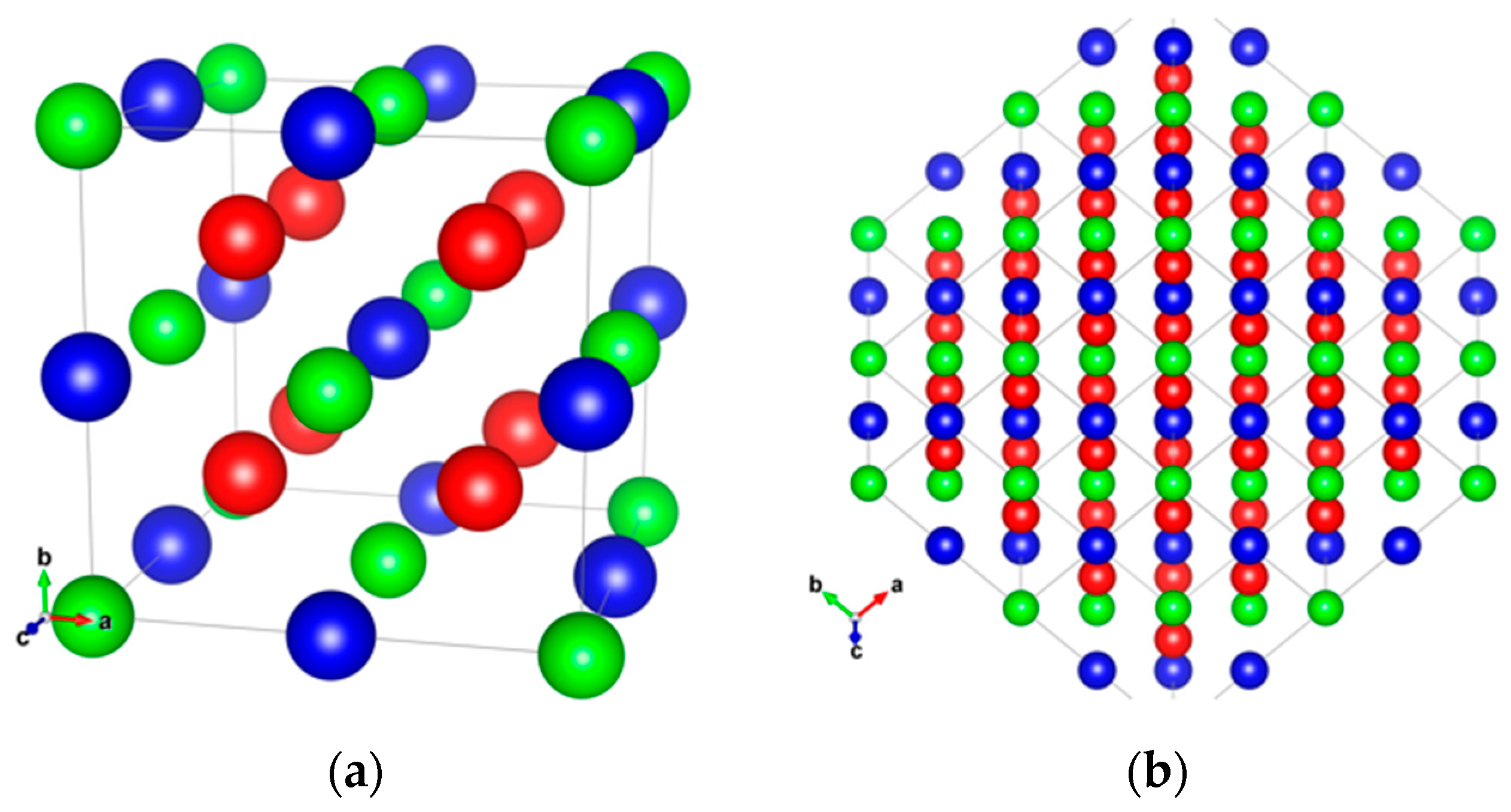
Figure 3.
Total spin magnetic moments per unit cell (Mt/f.u.) as a function of the total number of valence electrons in the unit cell for major Heusler alloys. The lines represent three different forms of the generalised Slater-Pauling curves [45].
Figure 3.
Total spin magnetic moments per unit cell (Mt/f.u.) as a function of the total number of valence electrons in the unit cell for major Heusler alloys. The lines represent three different forms of the generalised Slater-Pauling curves [45].
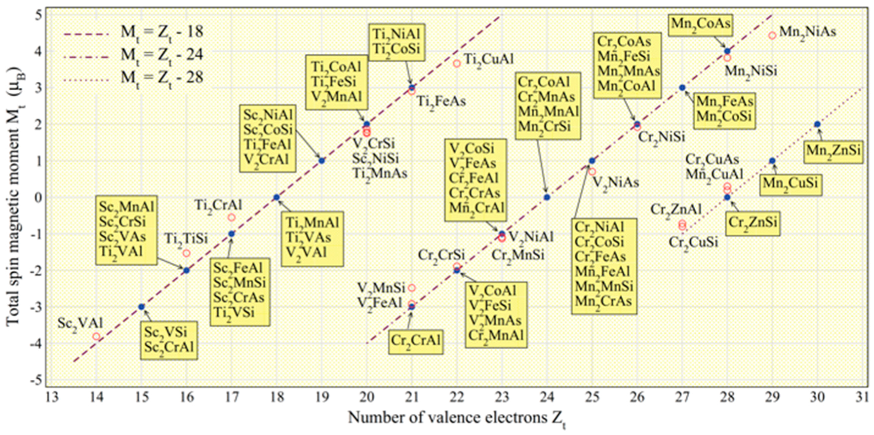
Figure 4.
(a) The ferrimagnetic structure of D022 Mn3Ga or D022 Mn3Ge. There is overall c-axis anisotropy but the structure is noncollinear and the 2b sublattice has a soft, in-plane component, which is indicated by small circles; (b) Ferromagnetic structure of L10 MnGa. The Mn atoms in the 4d positions all couple ferromagnetically [104]; (c) Perpendicular magnetoresistance (MR) loops for Mn0.62Ga0.38 (30)/Mg (0.4)/MgO (1.8)/CoFeB (1.2) (thickness in nm) measured at 300 K (blue solid squares) and 5 K (red open squares). The inset shows the temperature dependence of parallel and antiparallel resistances (RP and RAP) [102].

Figure 5.
Tunneling resistance, R, as a function of out-of-plane magnetic field, H, measured at RT and 10 K for a p-MTJ, consisting of Co2FeAl (1.2)/MgO (1.8)/Fe (0.1)/CoFeB (1.3) (thickness in nm). Wide arrows illustrate the magnetisation states (P or AP) of bottom and top electrodes. The dashed lines with arrows represent sweeping directions of the magnetic fields with different traces. The directions of the magnetisations of the bottom and top electrodes were determined from M–H loops by checking the differences in magnetic moments and switching fields, respectively [107].
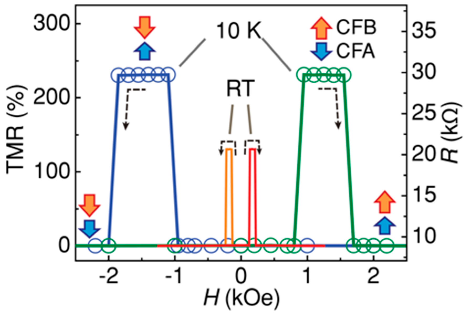
Figure 6.
(a) Magnetisation curves of a Co2FeSi film grown on a V seed layer, consisting of Si sub./V (25)/Co2FeSi (4)/V (1.5)/Ru (3) (thickness in nm) measured under the magnetic field application in-plane (red) and perpendicular to the plane (blue); (b) Magnetisation curves of a Co2FeSi film grown on a W seed layer, consisting of Si sub./W (25)/Co2FeSi (4)/W (1.5)/Ru (3) (thickness in nm) measured under the magnetic field application in-plane (red) and perpendicular to the plane (black).
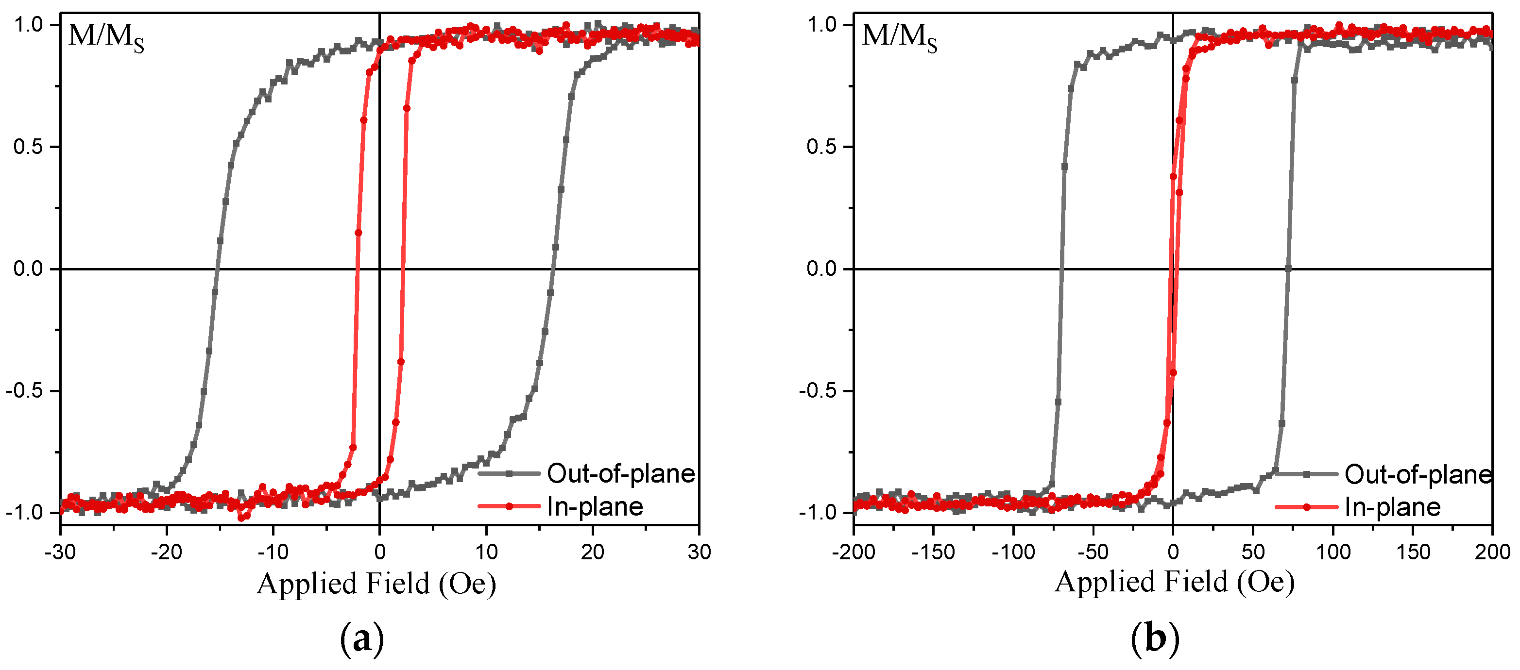
Figure 7.
(a) W lattice constants calculated from the W(110) peak positions measured by X-ray diffraction for the W-seed sample, consisting of Si sub./W (10)/Co2Fe Al0.5Si0.5 (12.5)/W (1.2)/Co2Fe Al0.5Si0.5 (2.5)/Ta (2) (thickness in nm), as a function of pre-growth heating between 300 ≤ T ≤ 370 K. The bulk value is shown as a reference. (b) Corresponding evolution of saturation magnetisation and coercivity (Hc) calculated from magnetisation curves.
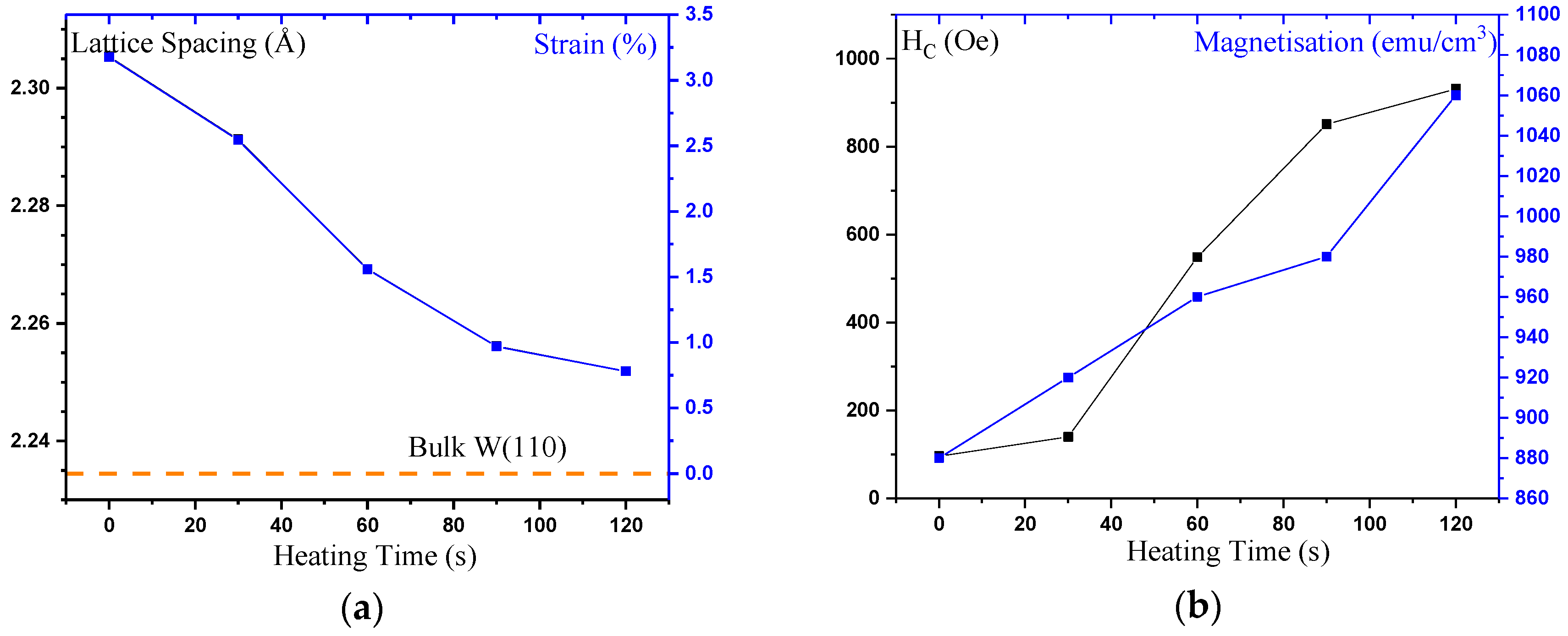
Figure 8.
(a) Current-perpendicular-to-the-plane giant magnetoresistance (CPP-GMR) effect measured under perpendicular fields for the (a) V- and (b) W-seed Co2FeSi junctions, consisting of W (10)/Co2FeAl0.5Si0.5 (12.5)/Ag(3)/Co2FeAl0.5Si0.5 (5) (thickness in nm) with dimensions of (a) (1000 × 500) μm2 and (b) (150 × 100) μm2.

Table 1.
List of measured saturation magnetisation (MS) and perpendicular magnetic anisotropy (PMA) for major Heusler alloys.
© 2018 by the authors. Licensee MDPI, Basel, Switzerland. This article is an open access article distributed under the terms and conditions of the Creative Commons Attribution (CC BY) license (http://creativecommons.org/licenses/by/4.0/).
Share and Cite
MDPI and ACS Style
Hirohata, A.; Frost, W.; Samiepour, M.; Kim, J.-y. Perpendicular Magnetic Anisotropy in Heusler Alloy Films and Their Magnetoresistive Junctions. Materials 2018, 11, 105. https://doi.org/10.3390/ma11010105
AMA Style
Hirohata A, Frost W, Samiepour M, Kim J-y. Perpendicular Magnetic Anisotropy in Heusler Alloy Films and Their Magnetoresistive Junctions. Materials. 2018; 11(1):105. https://doi.org/10.3390/ma11010105
Chicago/Turabian StyleHirohata, Atsufumi, William Frost, Marjan Samiepour, and Jun-young Kim. 2018. "Perpendicular Magnetic Anisotropy in Heusler Alloy Films and Their Magnetoresistive Junctions" Materials 11, no. 1: 105. https://doi.org/10.3390/ma11010105
Note that from the first issue of 2016, this journal uses article numbers instead of page numbers. See further details here.