Mie-Metamaterials-Based Thermal Emitter for Near-Field Thermophotovoltaic Systems

1
Department of Mechanical, Industrial and Systems Engineering, University of Rhode Island, Kingston, RI 02881, USA
2
College of Life Sciences, Northwest University, Xi’an 710069, China
3
National Engineering Research Center for Miniaturized Detection Systems, Northwest University, Xi’an 710069, China
*
Author to whom correspondence should be addressed.
Materials 2017, 10(8), 885; https://doi.org/10.3390/ma10080885
Submission received: 28 June 2017
/
Revised: 26 July 2017
/
Accepted: 29 July 2017
/
Published: 31 July 2017
(This article belongs to the Special Issue Advance in Plasmonics and Metamaterials)
Abstract
:In this work, we theoretically analyze the performance characteristics of a near-field thermophotovoltaic system consisting a Mie-metamaterial emitter and GaSb-based photovoltaic cell at separations less than the thermal wavelength. The emitter consists of a tungsten nanoparticle-embedded thin film of SiO deposited on bulk tungsten. Numerical results presented here are obtained using formulae derived from dyadic Green’s function formalism and Maxwell-Garnett-Mie theory. We show that via the inclusion of tungsten nanoparticles, the thin layer of SiO acts like an effective medium that enhances selective radiative heat transfer for the photons above the band gap of GaSb. We analyze thermophotovoltaic (TPV) performance for various volume fractions of tungsten nanoparticles and thicknesses of SiO.
1. Introduction
Thermophotovoltaics (TPVs) have been the focus of several works as an alternative to power generation technologies and a technology for waste heat recovery systems [1,2,3]. A typical TPV system consists of a high-temperature (∼1500 K) thermal emitter and a photovoltaic (PV) cell that converts the energy of incident photons into electricity. While ideal TPV systems convert radiative energy into electricity at an efficiency of the Carnot engine, practical TPV systems suffer from mismatch between the emission spectra of the emitter and absorption spectra of PV cell [4,5,6,7,8]. Several studies have investigated the use of metamaterials [9,10,11], surface gratings and photonics crystals [12,13,14,15,16,17], and complex surface patterns [18] to improve efficiency of TPV systems. In the last few years, it was demonstrated that near-field thermal radiation has a great potential in improving TPV systems [19,20,21,22,23,24]. Several theoretical studies were focused on exploiting near-field coupling of surface waves between emitter and PV cell at nanometer separation to improve the efficiency. It is challenging to develop materials that can withstand high temperatures as well as allow an enhanced coupling of surface waves for the energies above the band gap of the PV cell. One-dimensional gratings, hyperbolic metamaterials, and photonic crystals have shown a great potential in TPV applications. Dielectric mixtures and nanoparticle-embedded thin films can also be utilized to tune near-field thermal radiation [25]. It has been previously demonstrated that Mie-metamaterials or Mie-resonance metamaterials that utilize Mie resonances of inclusions into host materials can be used for spectral tuning of near-field thermal radiation. Authors demonstrated the possible use of tungsten nanoparticle-embedded thin film of SiO to achieve a selective thermal emitter for a far-field TPV system [26]. The effect of nanoparticle inclusions into host material on near-field radiative heat transfer has been investigated in several theoretical studies [27,28,29]. Stemming from earlier work, we demonstrate the use of a Mie-metamaterial thermal emitter that consists of tungsten nanoparticles embedded in a thin film of SiO deposited on a thick layer of tungsten for a near-field TPV system. We also explore possible alternative of W nanoparticles by refractive materials such as titanium nitride (TiN), tantalum (Ta), and molybdenum (Mo). We investigate the performance of such a TPV system for various configurations. While many recent works have dealt with gratings, photonic crystals, and other metamaterials, this is the first time nanoparticle-embedded thin films have been investigated for a near-field TPV system.
The configuration of the near-field TPV system considered in the present study is shown in Figure 1. The emitter side is a Mie-metamaterial consisting of tungsten nanoparticles embedded in SiO thin film on the top of a tungsten layer. The radius of the nanoparticles was fixed at 20 nm. The volume fraction and thickness of the SiO layer can be varied to investigate behaviour of the system. The layer of tungsten blocks radiation from the substrate, making the emitter essentially opaque. The PV cell considered here is GaSb (which has a bandgap of 0.726 eV), whose properties can be found in Reference [30]. Calculations reported in this work are for emitter temperature of 1500 K, while the PV cell is assumed to be at 300 K. The separation between the emitter and PV cell is comparable to or less than the thermal wavelength at 1500 K (= 1.93 m).
While we mostly concern ourselves with the theoretical side of the proposed thermal emitter, there are various ways to fabricate nanoparticle-embedded thin films. For example, it has been demonstrated that a stack of metallic nanoparticle arrays and SiO arrays can be fabricated [31]. Alternatively, as suggested by [32], core-shell nanoparticle arrays can be fabricated using tungsten core and SiO shell. This is followed by sputtering or chemical vapor deposition of SiO. W Nanoparticles-SiO composites can also be fabricated using sputtering deposition process [33,34,35]. A mixture of W and SiO powders can be prepared using PVDF (polyvinylidene fluoride) and sintering/pressing onto a sputtering cooling plate. W-SiO composites can be fabricated by RF sputtering of W followed by sputtering of W-SiO powder. During the sputtering process, tungsten nanoparticles would form.
2. Results and Discussion
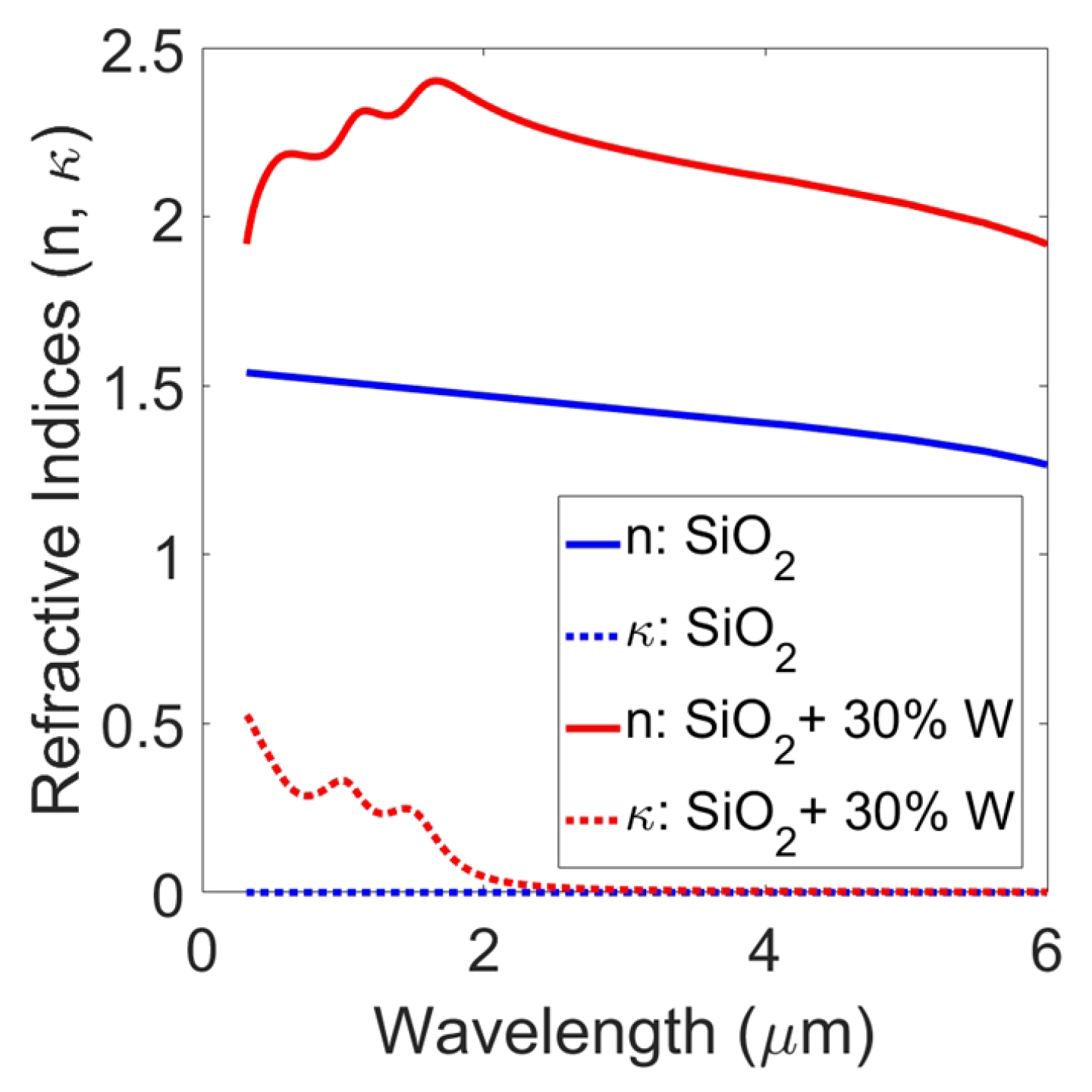
The refractive indices of plain SiO and that of SiO mixed with 30% nanoparticles of tungsten are shown in Figure 2. The effect of nanoparticle inclusions can be observed. SiO has a near-constant value of refractive index (n) and a negligible extinction coefficient () in the spectral range of our interest. The dielectric mixture of SiO and tungsten displayed an overall increased effective refractive index and a higher absorption coefficient for wavelengths shorter than 2.5 m.
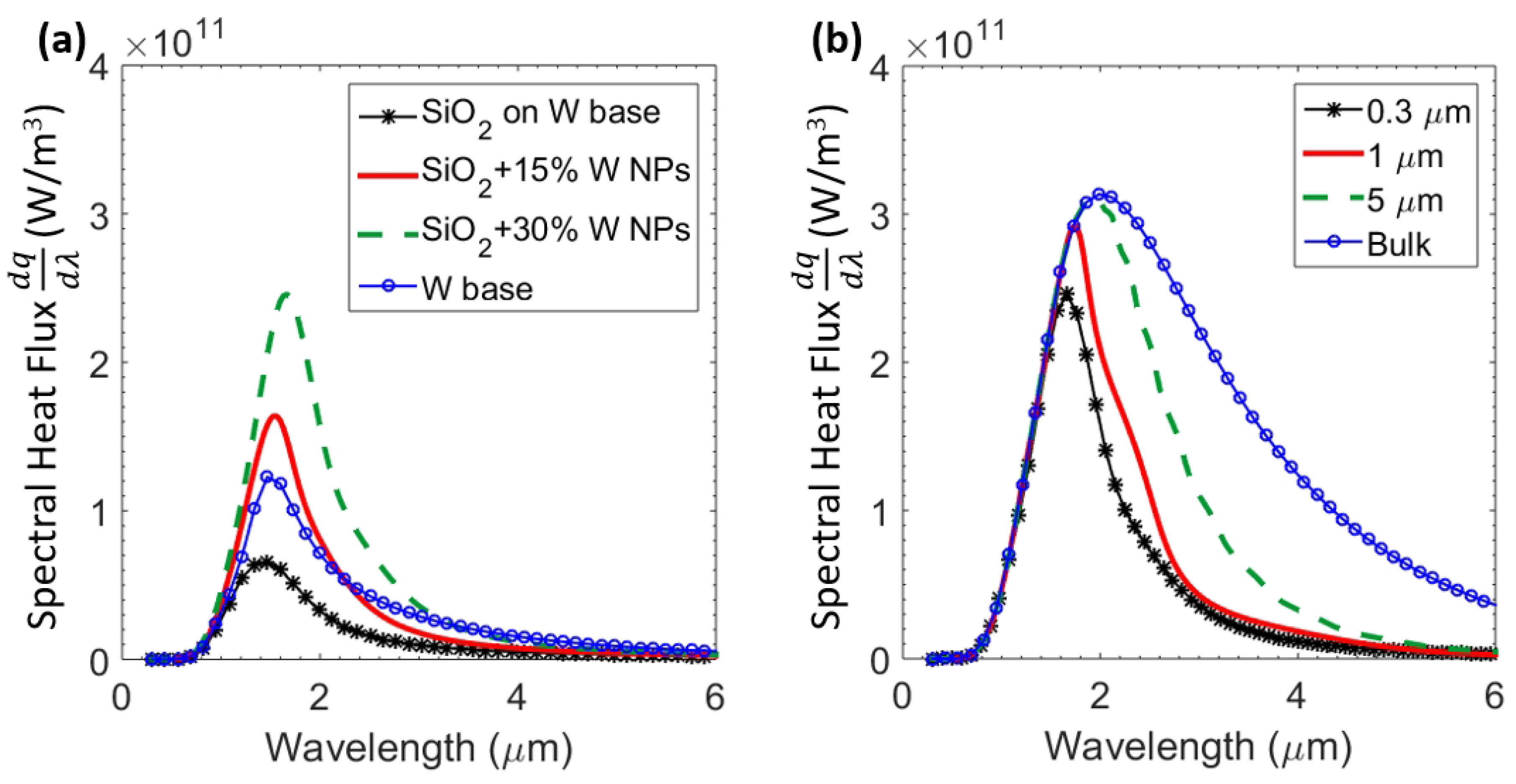
It is crucial to reduce the spectral energy below the band-gap of the PV cell in order to improve the overall thermal efficiency of the TPV system. The coupling of surface waves dictates whether radiative transfer would be enhanced or suppressed. The goal is to enhance radiative transfer above the bandgap without significantly enhancing radiation below the bandgap of the PV cell. In order to assess the impact of nanoparticle inclusions, we investigate the spectral heat flux of the proposed TPV system for various configurations. The spectral heat flux across the proposed thermal emitter at a separation of nm for various compositions is plotted in Figure 3. The emitter with a 0.3 m layer of SiO on tungsten had lower heat flux across the spectrum when compared to plain tungsten, as seen in Figure 3a. However, upon the inclusion of tungsten nanoparticles, spectral heat flux increased and was more selective towards shorter wavelengths ( m). While spectral heat flux showed an increase over the entire range, it was more prominent for energies above the band-gap, leading to a lesser fraction of energy lost. An increased absorption coefficient in the shorter wavelengths can be accounted for by enhanced coupling of surface modes in that range. To demonstrate the effect of reducing bulk layer to thin layer, Figure 3b illustrates spectral responses for various thicknesses of SiO layer and a fixed nanoparticle volume fraction of 30%. While a bulk layer of SiO mixed with tungsten nanoparticle showed broadband heat transfer, it can be clearly seen that thinner layers of SiO yielded more selective spectral response while maximum spectral heat flux remained relatively constant. It can be observed that radiation at longer wavelengths was more sensitive to layer thickness—such a configuration is more desirable for minimizing losses due to long-wavelength photons. In principle, it is possible to tune the near-field thermal radiation by changing the volume fraction of nanoparticles and thickness of the SiO layer to achieve optimal configuration for a given operating temperature and separation.
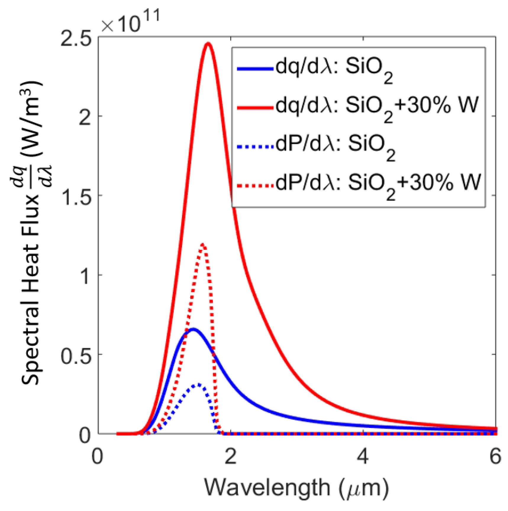
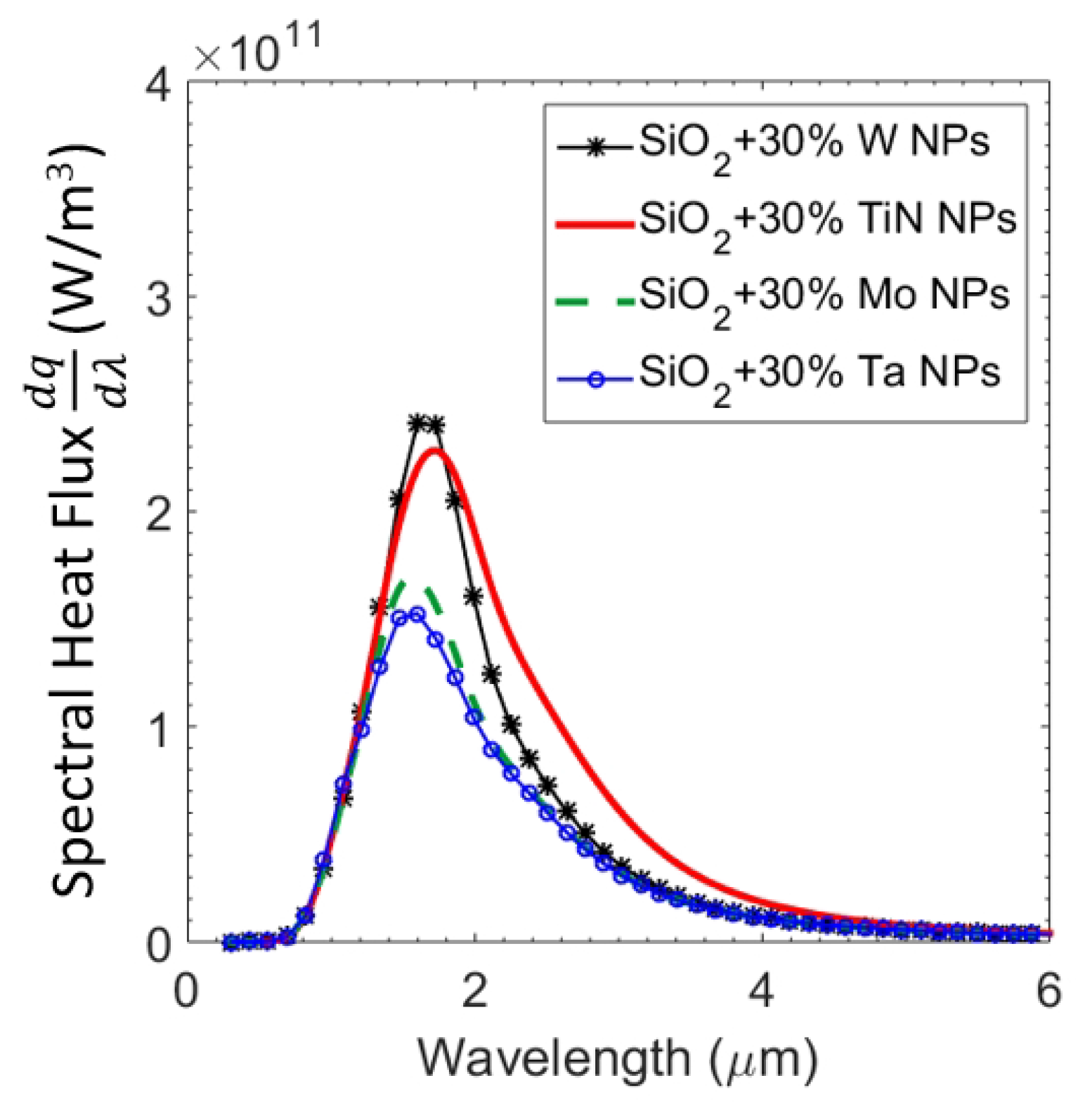
We now investigate the power output of the GaSb PV cell as a result of near-field radiative heat transfer at a separation of 100 nm. To assess the overall performance of the TPV system, we model the PV cell as discussed in Section 3. We calculate spectral density of output power along with the total output power. Figure 4 shows calculated spectral density of output power from the PV cell for the emitter with a pure SiO layer of 0.3 m thickness on tungsten and a SiO layer with 30% tungsten nanoparticles. The emitter with a tungsten nanoparticles-embedded thin film of SiO displayed an enhanced output power contribution above the bandgap of the GaSb PV cell when compared with the emitter with pure SiO layer. For comparison, the spectral heat flux across the interface of the same configurations are also shown. The total heat flux and total power output of the PV cell of these configurations are plotted against separation up to 10 nm in Figure 5. For gaps larger than 1 m (far-field), heat flux (and consequently power power and system efficiencies) were independent of the distance. For separations less than 1 m (near-field), the overall heat flux increased due to the presence of evanescent waves. Consequently, the output power also rose monotonically as separation between the emitter and PV cell was reduced. The inset in Figure 5 shows TPV system efficiency against distance for the same setups. While the trend in efficiencies is not as monotonous, for separations smaller than 100 nm, the emitter with tungsten nanoparticles showed higher thermal efficiency than the one with pure SiO. This is supported by earlier results that show the increased selectivity at shorter wavelengths leading to lower losses. Interestingly, the emitter with pure SiO had higher efficiency in the far-field. Nevertheless, such a configuration had lower output power. The oscillatory behaviour of efficiency has been observed before, and can be attributed to vacuum gap behaving like a waveguide [4]. We would like to emphasize that in order to further improve the performance of the TPV system, the materials chosen are not necessarily optimal. For example, PV cells with lower band gap (e.g., InGaAs and InGaSb or quaternary alloys like InGaAsSb) can be used. This can allow the use of lower emitter temperature or higher efficiencies and output power at the same operating temperatures. Alternatively, other materials, such as AlO (in place of SiO) and platinum, molybdenum, tantalum, and titanium nitride (in place of W) can be investigated for thermal emitter structure. We show a possible replacement of W by refractory materials such as titanium nitride (TiN), molybdenum (Mo), and tantalum (Ta) using our calculations in Figure 6. Spectral heat flux between the PV cell and emitter with SiO layer of 0.3 m thickness and 30% nanoparticles at a separation of 100 nm is shown. For comparison, heat flux with tungsten nanoparticles is shown. Corresponding values of total heat flux for W, TiN, Mo, and Ta nanoparticles were 3.72 × 10, 3.81 × 10, 2.68 × 10 and 2.57 × 10 W/m, respectively. From Figure 6 it appears that emitter with TiN and W nanoparticles displayed higher heat flux for this particular configuration. The emitter with tungsten nanoparticles showed better selectivity than TiN. Various combinations of material type and dimensions can be investigated to tune the emission spectra.
Overall, we have conducted the first numerical investigation of a near-field thermophotovoltaic system that uses a Mie-metamaterial-based thermal emitter and a PV cell at a separation less than the thermal wavelength. We have theoretically demonstrated an enhanced wavelength-selective thermal emitter for near-field thermophotovoltaic system using a Mie-resonance metamaterial. The thermal emitter consists of tungsten nanoparticle-embedded thin film of SiO deposited on a thick tungsten substrate. We analyzed the performance of such a TPV device for various cases. We studied the effect of volume fraction, layer thickness of SiO, and separation between emitter and PV cell. The embedded tungsten nanoparticles in the thin film can alter the refractive index of the film and allow spectral control of near-field radiative transfer across the emitter and the PV cell. We evaluated the energy conversion efficiency of the proposed near-field thermophotovoltaic system. The results show that the structure of the Mie-metamaterial thermal emitter can significantly improve the efficiency of the thermophotovoltaic system. Improvement in spectral selectivity as well as overall heat transfer can be attributed to increased power output and efficiency. We showed that by changing the volume fraction of nanoparticles and the thickness of the SiO layer, it is possible to tune the near-field thermal radiation to obtain enhanced output power and high thermal efficiency. The materials considered can withstand high temperatures and are suitable for thermal emitters.
3. Materials and Methods
The expression of radiative transfer between closely-spaced bodies can be derived using dyadic Green’s function approach [36], and is given by
where is the energy of a harmonic oscillator at frequency , temperature T, ћ is the reduced Planck constant, and is the Boltzmann constant. The function corresponds to the spectral transmissivity in radiative transfer between media 1 and 2 separated by distance L and is expressed as [36]
where and are polarized effective reflection coefficients of the two half spaces (calculated in the absence of other half space), and is the z-component of wavevector in vacuum. The first term in Equation (2) corresponds to propagating waves, while the second term describes the thermal transport due to evanescent waves, and its contribution is significant only for small values of gap L. For a structure having N-layer media having interfaces, the expression for the generalized reflection coefficient at the interface between region i and region is given by [37]:
where is the Fresnel reflection coefficient at the interface between layers i and , and is the generalized reflection coefficient at the interface between layers and , (or p) refers to transverse electric (or magnetic) polarization, is the location of the ith interface. is the normal z-component of the wave vector in medium i, wherein is the relative permittivity of the medium i as a function of angular frequency , c is the speed of light in vacuum, and is the magnitude of the in-plane wave vector. With , the above equation provides a recursive relation to calculate the reflection coefficients in all regions. To calculate the effective dielectric function of the Mie-metamaterial, we use the Clausius–Mossotti equation [38,39].
where is the dielectric function of the matrix, is the electric dipole polarizability, and r and f are the radius and volume fraction of nanoparticles, respectively. To consider the size effects of nanoparticle inclusions, we use the Maxwell-Garnett formula, which employs the expression for electric dipole polarizability using Mie theory [40], , where is the first electric Mie coefficient given by
where and are Riccati–Bessel functions of the first order given by and where and are first-order spherical Bessel functions and spherical Hankel functions of the first kind, respectively. Here, “” indicates the first derivative. and are the size parameters of the matrix and the nanoparticles, respectively; is the dielectric function of nanoparticles. It is worth mentioning that Maxwell-Garnett-Mie theory is applicable when the average distance between inclusions is much smaller than the wavelength of interest [41]. This criteria is satisfied in the calculations presented. Since nanoparticle diameter (40 nm) is much smaller than the thickness of the thin film (0.3 m) considered, effective medium theory holds true for the calculations presented in this study. Dielectric functions of the materials (SiO and W) considered in this paper are taken from literature [42,43]. Having very low temperature coefficients, room temperature values of dielectric function are used for SiO [44]. Dielectric properties of tungsten were also assumed to be unchanged, as the operating temperature is much less than the melting point.
Near-field thermal radiation and charge transport in PV cell can be theoretically modelled by accounting for charge density distribution due to the number of photons absorbed at different cell depths [22]. Due to the limitations of the present study, we employ a simplistic model to calculate the output power of a PV cell. We assume that quantum efficiency of a PV cell in the near-field would be the same as that in the far-field. Therefore, short circuit current can be calculated as [22]
where is the bandgap of GaSb cell, is external quantum efficiency, is spectral heat flux, and e is the electronic charge. Dark current can be calculated by
where and are diffusivities of electrons and holes, respectively, is the intrinsic carrier concentration, and are concentrations of electrons and holes, respectively, while diffusion lengths and can be calculated in terms of diffusivity and recombination lifetime using
Total recombination lifetime is calculated by
where , , and are radiative recombination, Shockley–Hall recombination, and Augar recombination, respectively [45]. Open circuit voltage is calculated using
Output power of the PV cell is given by
where and efficiency of the TPV system is given by
For our calculations, intrinsic carrier concentration was assumed to be cm. Carrier concentration of electrons and holes were assumed to be equal to cm. The recombination lifetimes are taken to be ns, ns, and s. Carrier diffusivities are cms and cm/s for electrons and holes, respectively.
Acknowledgments
This project was supported in part by an Institutional Development Award (IDeA) Network for Biomedical Research Excellence from the National Institute of General Medical Sciences of the National Institutes of Health under grant number P20GM103430, Rhode Island STAC Research Grant number AWD05085, and Rhode Island Foundation Research Grant number 20164342.
Author Contributions
A.G. did the calculations and wrote the paper. Y.T. contributed to analysis of the results and writing the paper. S.Z. and Y.C. contributed to discussion of the results and writing the paper. Y.Z. supervised the project. All authors discussed the results and commented on the manuscript.
Conflicts of Interest
The authors declare no conflict of interest.
References
- Basu, S.; Chen, Y.; Zhang, Z. Microscale radiation in thermophotovoltaic devices-a review. Int. J. Energy Res. 2007, 31, 689–716. [Google Scholar] [CrossRef]
- Bosi, M.; Ferrari, C.; Melino, F.; Pinelli, M.; Spina, P.; Venturini, M. Thermophotovoltaic generation: A state of the art review. In Proceedings of the 25th International Conference on Efficiency, Cost, Optimization and Simulation of Energy Conversion Systems and Processes, Perugia, Italy, 26–29 June 2012. [Google Scholar]
- Coutts, T. A review of progress in thermophotovoltaic generation of electricity. Renew. Sustain. Energy Rev. 1999, 3, 77–184. [Google Scholar] [CrossRef]
- Tong, J.K.; Hsu, W.C.; Huang, Y.; Boriskina, S.V.; Chen, G. Thin-film ‘thermal well’emitters and absorbers for high-efficiency thermophotovoltaics. Sci. Rep. 2015, 5, 10661. [Google Scholar] [CrossRef] [PubMed]
- Harder, N.P.; Würfel, P. Theoretical limits of thermophotovoltaic solar energy conversion. Semicond. Sci. Technol. 2003, 18, S151. [Google Scholar] [CrossRef]
- Rephaeli, E.; Fan, S. Absorber and emitter for solar thermo-photovoltaic systems to achieve efficiency exceeding the Shockley-Queisser limit. Opt. Express 2009, 17, 15145–15159. [Google Scholar] [CrossRef] [PubMed]
- Wurfel, P.; Ruppel, W. Upper limit of thermophotovoltaic solar-energy conversion. IEEE Trans. Electron Devices 1980, 27, 745–750. [Google Scholar] [CrossRef]
- Bermel, P.; Ghebrebrhan, M.; Chan, W.; Yeng, Y.X.; Araghchini, M.; Hamam, R.; Marton, C.H.; Jensen, K.F.; Soljačić, M.; Joannopoulos, J.D.; et al. Design and global optimization of high-efficiency thermophotovoltaic systems. Opt. Express 2010, 18, A314–A334. [Google Scholar] [CrossRef] [PubMed]
- Liu, X.; Tyler, T.; Starr, T.; Starr, A.F.; Jokerst, N.M.; Padilla, W.J. Taming the blackbody with infrared metamaterials as selective thermal emitters. Phys. Rev. Lett. 2011, 107, 045901. [Google Scholar] [CrossRef] [PubMed]
- Wu, C.; Neuner, B., III; John, J.; Milder, A.; Zollars, B.; Savoy, S.; Shvets, G. Metamaterial-based integrated plasmonic absorber/emitter for solar thermo-photovoltaic systems. J. Opt. 2012, 14, 024005. [Google Scholar] [CrossRef]
- Molesky, S.; Dewalt, C.J.; Jacob, Z. High temperature epsilon-near-zero and epsilon-near-pole metamaterial emitters for thermophotovoltaics. Opt. Express 2013, 21, A96–A110. [Google Scholar] [CrossRef] [PubMed]
- Nagpal, P.; Han, S.E.; Stein, A.; Norris, D.J. Efficient low-temperature thermophotovoltaic emitters from metallic photonic crystals. Nano Lett. 2008, 8, 3238–3243. [Google Scholar] [CrossRef] [PubMed]
- Arpin, K.A.; Losego, M.D.; Cloud, A.N.; Ning, H.; Mallek, J.; Sergeant, N.P.; Zhu, L.; Yu, Z.; Kalanyan, B.; Parsons, G.N.; et al. Three-dimensional self-assembled photonic crystals with high temperature stability for thermal emission modification. Nat. Commun. 2013, 4. [Google Scholar] [CrossRef] [PubMed]
- Heinzel, A.; Boerner, V.; Gombert, A.; Bläsi, B.; Wittwer, V.; Luther, J. Radiation filters and emitters for the NIR based on periodically structured metal surfaces. J. Mod. Opt. 2000, 47, 2399–2419. [Google Scholar] [CrossRef]
- Fleming, J.; Lin, S.; El-Kady, I.; Biswas, R.; Ho, K. All-metallic three-dimensional photonic crystals with a large infrared bandgap. Nature 2002, 417, 52–55. [Google Scholar] [CrossRef] [PubMed]
- Sai, H.; Kanamori, Y.; Yugami, H. Tuning of the thermal radiation spectrum in the near-infrared region by metallic surface microstructures. J. Micromech. Microeng. 2005, 15, S243. [Google Scholar] [CrossRef]
- Ghanekar, A.; Sun, M.; Zhang, Z.; Zheng, Y. Optimal Design of Wavelength Selective Thermal Emitter for Thermophotovoltaic Applications. J. Therm. Sci. Eng. Appl. 2007, 10, 011004. [Google Scholar]
- Woolf, D.; Hensley, J.; Cederberg, J.; Bethke, D.; Grine, A.; Shaner, E. Heterogeneous metasurface for high temperature selective emission. Appl. Phys. Lett. 2014, 105, 081110. [Google Scholar] [CrossRef]
- Narayanaswamy, A.; Chen, G. Surface modes for near field thermophotovoltaics. Appl. Phys. Lett. 2003, 82, 3544–3546. [Google Scholar] [CrossRef]
- DiMatteo, R.; Greiff, P.; Seltzer, D.; Meulenberg, D.; Brown, E.; Carlen, E.; Kaiser, K.; Finberg, S.; Nguyen, H.; Azarkevich, J.; et al. Micron-gap T hermo P hoto V oltaics (MTPV). AIP Conf. Proc. 2004, 738, 42–51. [Google Scholar]
- Laroche, M.; Carminati, R.; Greffet, J.J. Near-field thermophotovoltaic energy conversion. J. Appl. Phys. 2006, 100, 063704. [Google Scholar] [CrossRef]
- Park, K.; Basu, S.; King, W.P.; Zhang, Z. Performance analysis of near-field thermophotovoltaic devices considering absorption distribution. J. Quant. Spectrosc. Radiat. Transf. 2008, 109, 305–316. [Google Scholar] [CrossRef]
- Francoeur, M.; Vaillon, R.; Mengüç, M.P. Thermal impacts on the performance of nanoscale-gap thermophotovoltaic power generators. IEEE Trans. Energy Convers. 2011, 26, 686–698. [Google Scholar] [CrossRef]
- Bright, T.; Wang, L.; Zhang, Z. Performance of near-field thermophotovoltaic cells enhanced with a backside reflector. J. Heat Transf. 2014, 136, 062701. [Google Scholar] [CrossRef]
- Ghanekar, A.; Lin, L.; Su, J.; Sun, H.; Zheng, Y. Role of nanoparticles in wavelength selectivity of multilayered structures in the far-field and near-field regimes. Opt. Express 2015, 23, A1129–A1139. [Google Scholar] [CrossRef] [PubMed]
- Ghanekar, A.; Lin, L.; Zheng, Y. Novel and efficient Mie-metamaterial thermal emitter for thermophotovoltaic systems. Opt. Express 2016, 24, A868–A877. [Google Scholar] [CrossRef] [PubMed]
- Francoeur, M.; Basu, S.; Petersen, S.J. Electric and magnetic surface polariton mediated near-field radiative heat transfer between metamaterials made of silicon carbide particles. Opt. Express 2011, 19, 18774–18788. [Google Scholar] [CrossRef] [PubMed]
- Zhao, Q.; Zhou, J.; Zhang, F.; Lippens, D. Mie resonance-based dielectric metamaterials. Mater. Today 2009, 12, 60–69. [Google Scholar] [CrossRef]
- Wheeler, M.S.; Aitchison, J.S.; Mojahedi, M. Three-dimensional array of dielectric spheres with an isotropic negative permeability at infrared frequencies. Phys. Rev. B 2005, 72, 193103. [Google Scholar] [CrossRef]
- Adachi, S. Optical dispersion relations for GaP, GaAs, GaSb, InP, InAs, InSb, AlxGa1-xAs, and In1-xGaxAsyP1-y. J. Appl. Phys. 1989, 66, 6030–6040. [Google Scholar] [CrossRef]
- Ji, T.; Peng, L.; Zhu, Y.; Yang, F.; Cui, Y.; Wu, X.; Liu, L.; He, S.; Zhu, F.; Hao, Y. Plasmonic broadband absorber by stacking multiple metallic nanoparticle layers. Appl. Phys. Lett. 2015, 106, 161107. [Google Scholar] [CrossRef]
- Sakurai, A.; Kawamata, T. Electromagnetic resonances of solar-selective absorbers with nanoparticle arrays embedded in a dielectric layer. J. Quant. Spectrosc. Radiat. Transf. 2016, 184, 353–359. [Google Scholar] [CrossRef]
- Reed, J.S. Principles of Ceramics Processing; Wiley: Hoboken, NJ, USA, 1995. [Google Scholar]
- Sahoo, P.K.; Kamal, S.K.; Premkumar, M.; Kumar, T.J.; Sreedhar, B.; Singh, A.; Srivastava, S.; Sekhar, K.C. Synthesis of tungsten nanoparticles by solvothermal decomposition of tungsten hexacarbonyl. Int. J. Refract. Met. Hard Mater. 2009, 27, 784–791. [Google Scholar] [CrossRef]
- Rodriguez-Suarez, T.; Diaz, L.; Lopez-Esteban, S.; Pecharroman, C.; Esteban-Cubillo, A.; Gremillard, L.; Torrecillas, R.; Moya, J. Epitaxial growth of tungsten nanoparticles on alumina and spinel surfaces. Nanotechnology 2008, 19, 215605. [Google Scholar] [CrossRef] [PubMed]
- Narayanaswamy, A.; Zheng, Y. A Green’s function formalism of energy and momentum transfer in fluctuational electrodynamics. J. Quant. Spectrosc. Radiat. Transf. 2014, 132, 12–21. [Google Scholar] [CrossRef]
- Chew, W.C. Waves and Fields in Inhomogeneous Media; IEEE Press: New York, NY, USA, 1995. [Google Scholar]
- Myroshnychenko, V.; Rodríguez-Fernández, J.; Pastoriza-Santos, I.; Funston, A.M.; Novo, C.; Mulvaney, P.; Liz-Marzán, L.M.; de Abajo, F.J.G. Modelling the optical response of gold nanoparticles. Chem. Soc. Rev. 2008, 37, 1792–1805. [Google Scholar] [CrossRef] [PubMed]
- Kreibig, U.; Vollmer, M. Optical Properties of Metal Clusters; Springer: Berlin, Germany, 1995; Volume 25. [Google Scholar]
- Doyle, W.T. Optical properties of a suspension of metal spheres. Phys. Rev. B 1989, 39, 9852. [Google Scholar] [CrossRef]
- Wheeler, M.S. A Scattering-Based Approach to the Design, Analysis, and Experimental Verification of Magnetic Metamaterials Made from Dielectrics. Ph.D. Thesis, University of Toronto, Toronto, ON, Canada, 2010. [Google Scholar]
- Gao, L.; Lemarchand, F.; Lequime, M. Refractive index determination of SiO2 layer in the UV/Vis/NIR range: Spectrophotometric reverse engineering on single and bi-layer designs. J. Eur. Opt. Soc.-Rapid Publ. 2013, 8, 13010. [Google Scholar] [CrossRef]
- Rakić, A.D.; Djurišić, A.B.; Elazar, J.M.; Majewski, M.L. Optical properties of metallic films for vertical-cavity optoelectronic devices. Appl. Opt. 1998, 37, 5271–5283. [Google Scholar] [CrossRef] [PubMed]
- Timans, P. Advances in Rapid Thermal and Integrated Processing; Roozeboom, F., Ed.; Kluwer Academic Publishers: Dordrecht, The Netherlands, 1996. [Google Scholar]
- McKelvey, J.P. Solid State and Semiconductor Physics; Harper & Row: Manhattan, NY, USA, 1966. [Google Scholar]
Figure 1.
Schematic of near-field thermophotovoltaic system consisting of the proposed thermal emitter and GaSb-based PV cell at separation less than the thermal wavelength.
Figure 1.
Schematic of near-field thermophotovoltaic system consisting of the proposed thermal emitter and GaSb-based PV cell at separation less than the thermal wavelength.
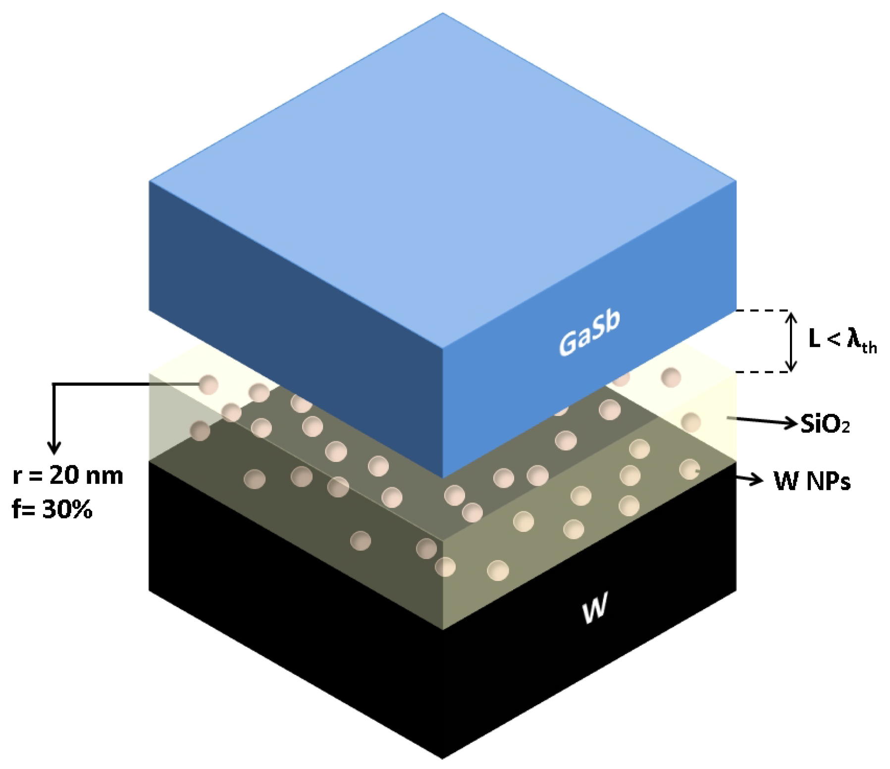
Figure 2.
Real (n) and imaginary () parts of refractive indices of pure SiO and SiO with 30% tungsten nanoparticles.
Figure 2.
Real (n) and imaginary () parts of refractive indices of pure SiO and SiO with 30% tungsten nanoparticles.

Figure 3.
Spectral heat flux across the proposed emitter and the GaSb photovoltaic (PV) cell at a separation of L = 100 nm for (a) various volume fractions of W nanoparticles—0%, 15% and 30%—compared to bulk W emitter; (b) Various thicknesses of SiO layer—0.3 m, 1 m, 5 m, and bulk respectively.
Figure 3.
Spectral heat flux across the proposed emitter and the GaSb photovoltaic (PV) cell at a separation of L = 100 nm for (a) various volume fractions of W nanoparticles—0%, 15% and 30%—compared to bulk W emitter; (b) Various thicknesses of SiO layer—0.3 m, 1 m, 5 m, and bulk respectively.

Figure 4.
Predicted spectral density of output power (dashed lines) from GaSb PV cell for emitter with pure SiO thin film and SiO with 30% of W nanoparticles for a separation of 100 nm compared with corresponding spectral heat fluxes (solid lines).
Figure 4.
Predicted spectral density of output power (dashed lines) from GaSb PV cell for emitter with pure SiO thin film and SiO with 30% of W nanoparticles for a separation of 100 nm compared with corresponding spectral heat fluxes (solid lines).

Figure 5.
Total heat flux (solid lines) and output power (dashed lines) of PV cell as a function of separation between the emitter and PV cell for an emitter of pure SiO film of 0.5 m and SiO films with W nanoparticles. Inset shows overall efficiency of the corresponding thermophotovoltaic (TPV) systems plotted as a function of separation. NP: nanoparticle.
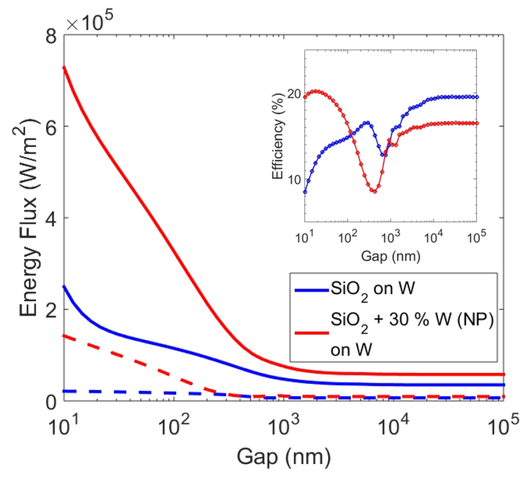
Figure 6.
Spectral heat flux across the emitter consisting of nanoparticles of alternative materials and the GaSb PV cell at a separation of nm for a nanoparticles volume fraction of 30%.
Figure 6.
Spectral heat flux across the emitter consisting of nanoparticles of alternative materials and the GaSb PV cell at a separation of nm for a nanoparticles volume fraction of 30%.

© 2017 by the authors. Licensee MDPI, Basel, Switzerland. This article is an open access article distributed under the terms and conditions of the Creative Commons Attribution (CC BY) license (http://creativecommons.org/licenses/by/4.0/).
Share and Cite
MDPI and ACS Style
Ghanekar, A.; Tian, Y.; Zhang, S.; Cui, Y.; Zheng, Y. Mie-Metamaterials-Based Thermal Emitter for Near-Field Thermophotovoltaic Systems. Materials 2017, 10, 885. https://doi.org/10.3390/ma10080885
AMA Style
Ghanekar A, Tian Y, Zhang S, Cui Y, Zheng Y. Mie-Metamaterials-Based Thermal Emitter for Near-Field Thermophotovoltaic Systems. Materials. 2017; 10(8):885. https://doi.org/10.3390/ma10080885
Chicago/Turabian StyleGhanekar, Alok, Yanpei Tian, Sinong Zhang, Yali Cui, and Yi Zheng. 2017. "Mie-Metamaterials-Based Thermal Emitter for Near-Field Thermophotovoltaic Systems" Materials 10, no. 8: 885. https://doi.org/10.3390/ma10080885
Note that from the first issue of 2016, this journal uses article numbers instead of page numbers. See further details here.