Tunable Multiple Plasmon-Induced Transparencies Based on Asymmetrical Grapheme Nanoribbon Structures

1
School of Science, Jiangsu Provincial Research Center of Light Industrial Optoelectronic Engineering and Technology, Jiangnan University, Wuxi 214122, China
2
Science and Technology on Electronic Test and Measurement Laboratory, North University of China, No. 3 Xueyuan Road, Taiyuan 030051, China
3
School of Physics and Optoelectronic Engineering, Nanjing University of Information Science & Technology, Nanjing 210044, China
*
Author to whom correspondence should be addressed.
Materials 2017, 10(7), 699; https://doi.org/10.3390/ma10070699
Submission received: 10 May 2017
/
Revised: 21 June 2017
/
Accepted: 23 June 2017
/
Published: 26 June 2017
(This article belongs to the Special Issue Advances in Transparent Conducting Materials)
Abstract
:We present plasmonic devices, consisting of periodic arrays of graphene nanoribbons (GNRs) and a graphene sheet waveguide, to achieve controllable plasmon-induced transparency (PIT) by numerical simulation. We analyze the bright and dark elements of the GNRs and graphene-sheet waveguide structure. Results show that applying the gate voltage can electrically tune the PIT spectrum. Adjusting the coupling distance and widths of GNRs directly results in a shift of transmission dips. In addition, increased angle of incidence causes the transmission to split into multiple PIT peaks. We also demonstrate that PIT devices based on graphene plasmonics may have promising applications as plasmonic sensors in nanophotonics.
1. Introduction
The electromagnetically induced transparency (EIT) effect observed in atomic systems produces a sharp and transparent window in a wide range of absorption spectra range. It results from a considerable hindrance between coherent optical transitions [1,2,3,4]. In the transparency window, there is obvious normal dispersion and ultrahigh quality factor, due to which, many feasible applications in optical storage, slow light, and other nonlinear processes based on the atomic EIT have been proposed [5]. In many optical structures, analogs of EIT have been presented [6,7,8,9,10,11]. In plasmonic systems, this effect is named plasmon-induced transparency (PIT); it can be realized by the considerable hindrance between bright and dark modes [8].
Graphene is a monolayer of carbon atoms with a honeycomb-like lattice that is gaining considerable attention because of its excellent electrical and photonic properties, such as strong optical nonlinearity [12], ultrahigh electron mobility [13], and high-thermal conductivity [14]. In particular, the surface conductivity of graphene can be changed by gate voltage, electromagnetic fields, and chemical doping [15,16,17,18]. In this way, the development of tunable plasmonic devices could be promoted. Considering these characteristic properties, graphene can also support propagation of surface plasmon polaritons (SPPs). Graphene surface plasmon polaritons (GSPPs) can be excited for a broad range of frequencies from near-infrared to the terahertz region [19]. Meanwhile, due to its high-carrier mobility, GSPPs display lower propagation loss at room temperature [20]. Moreover, adjusting the chemical potential of graphene can easily influence the propagation of GSPPs. Re-fabricating the structure is not necessary anymore. There have been many applications based on graphene, including absorbers [21], electro-optical switches [22], field-effect transistors [23], amplifiers [24], diodes [25], terahertz antennas [26], filters [27], mixers [28], plasmonic Bragg reflectors [29], and so on. A graphene-based plasmonic analog to EIT nanostructures has already been numerically illustrated by Shi et al. [30]. Consequently, the graphene becomes an advanced material in tunable PIT device design.
In this study, the coupling-induced transparency with narrow waveband can be exhibited by a properly designed system based on graphene-contained plasmonic structures by numerical simulation. Compared to previous works, we show the multiple PIT phenomena with our novel asymmetrical graphene nanoribbon structures and integrally analyze the influence factors of the PIT phenomena. First, the bright and dark elements of the GNRs and graphene sheet waveguide structure are analyzed. We observe the PIT phenomenon by presenting the structure devices composed of periodic arrays of GNRs and a graphene sheet. The shift of the transmission notch occurs because of the changes of the coupling distance and the widths of GNRs. The Fermi energy strongly influences the frequencies of plasmons in graphene. In addition, multiple PIT peaks can be obtained by changing the angle of incidence.
2. Materials Model and Analysis
Figure 1 shows the first schematic of the structure employed in our design. The gap g is sandwiched by the GNRs and graphene sheet layers. (For simplicity, the surrounding material is treated as air, εr = 1.) A transverse-magnetic (TM) polarization (magnetic field is parallel to the y-axis) monochromatic plane wave comes normally from the upper surface of the structure. p is the cycle of the unit element; w1 and w2 are the widths of the adjacent GNRs, and d is the distance. The designed device is easy to fabricate. The chemical vapour deposition (CVD) method can be utilized to grow multiple layers of graphene on the silica layer and to manufacture the silicon-based graphene structure waveguide. The momentum relaxation time τ, temperature T, incident wavelength λ, and Fermi energy Ef determine the surface conductivity of graphene σg. It follows the equation
In our simulation, the incident light we employed is at the range of the mid-infrared region. The intraband transition contribution predominates in monolayer graphene [31]. With this understanding, the optical conductivity is given by [32]
Here, e is the electron charge and the electron relaxation time is τ = μEF = evF2, in which vF = c/300 is the Fermi velocity; EF is the Fermi energy, and μ = 10 m2/(V·S) is the direct current mobility of graphene [33,34,35]. The graphene layers are viewed as an ultrathin film with the permittivity expressed as
where t0 = 1 nm is the thickness of the graphene layers. The SPPs modes, ranging from THz to the visible frequencies, could be spread over the graphene layer. The dispersion relation of the SPP modes at subwavelength scale is given by [36]
where kg is the in-plane wave vector in graphene, k0 is the wave vector in vacuum. ε1 and ε2 are the dielectric constants of the top and bottom surface materials of the graphene sheet, respectively. The graphene Fermi level can be tuned by adjusting the gate voltage, which can be calculated according to Equation (2).
3. Simulation and Results
To demonstrate the graphene-based PIT phenomenon, we start with nanostructures with different radiation performances, as is shown in Figure 2a,b: bright and dark elements. The resonant plasmonic modes in the bright and dark elements separately exhibit different coupling strengths to free space. The bright modes are excited by the bright element, which consists of two GNRs lying periodically along the x direction with different: widths w1 and w2. The dark modes are simply graphene sheet layers. The separation between the GNRs and graphene sheet layers is g. To realize the PIT phenomenon, the basic unit of the structure can be formed by combining the bright element with the dark element.
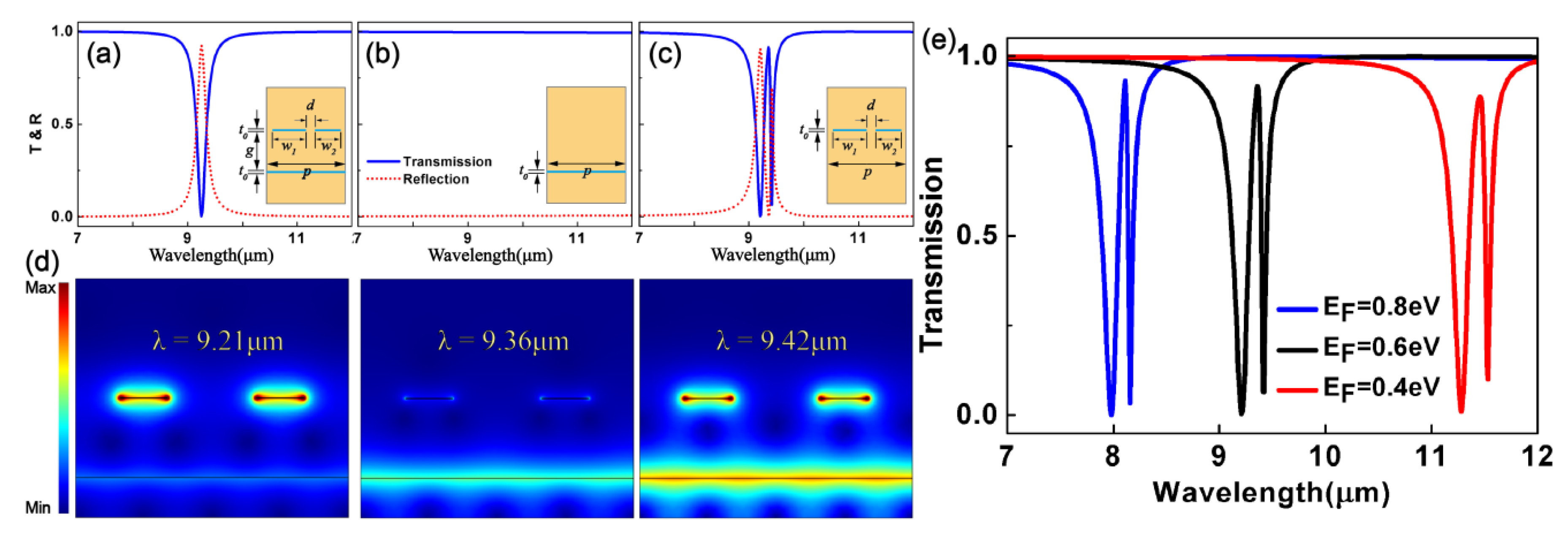
To study the PIT phenomenon in graphene nanostructures, we set up a graphene PIT structure, which is constructed by combining the coupled bright element with the dark element as the basic unit. The units array periodically with a period p = 1200 nm. Figure 2c shows the transmission and reflection spectra that we simulated at normal incidence for the graphene PIT structure.
Obviously, a PIT-like transparent window can be observed from the transmission spectrum of the graphene PIT structure. The two notches’ wavelengths are at 9.21 and 9.42 μm, and the peak is positioned at 9.36 μm. This phenomenon is essentially analogous to the EIT spectrum in atomic systems. At the PIT peak, almost no reflection can be observed. At the right transmission dip, the reflection is obviously low, revealing a strong absorption. In addition, to make the disturbance between the dark and bright modes visible, we exhibit the |E| distributions at these concerned wavelengths. The dipole mode can be effectively excited at the transparent peak by the incident light of 9.36 μm, while the excitation of the quadruple mode is prevented in the dark element. However, the coupling between the bright and dark modes can indirectly inspire the dark mode. The dark mode will then couple to the bright mode again. It is noticed that a phase difference of π occurs between the channels of the direct and indirect excitations [8,37]. Therefore, there is a mutual destructive interference between the bright and dark modes. Furthermore, the fields in the bright element are restrained, which causes a transparent window, similar to the EIT phenomenon in the atom. By comparison, the interference is beneficial to the enhancement of the fields in both elements at the transmission notches.
The optical performances of graphene can be considerably improved by doping or gating as plasmons in graphene are greatly dependent on the Fermi energy. By adjusting the Fermi energy, the electron density in graphene can be changed, resulting in a change in the resonance frequencies of graphene plasmonic nanostructures. As a result, the PIT spectrum of the graphene PIT structure can be dynamically controlled over a wide range of wavelengths. Such tunability can be hard to realize in atomic EIT or other PIT systems. The transmission spectra for structure I at different EF are plotted in Figure 2e. The PIT transparency windows can be blue-shifted obviously while EF changes from 0.4 to 0.8 eV. Therefore, the PIT spectrum can be shifted over a rather wide range of wavelengths by tuning the Fermi energy.
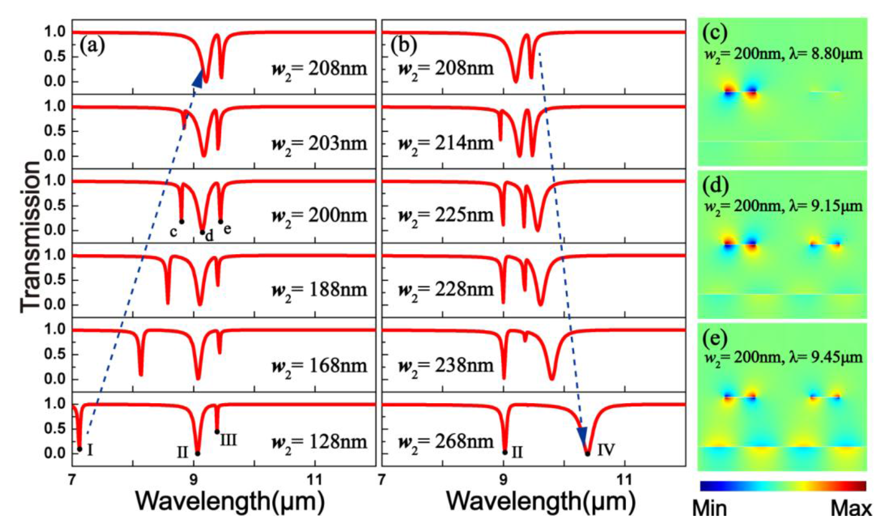
The transmission spectra of structure I are shown in Figure 3a,b. Here, p = 1200 nm, w1 = 208 nm, g = 350 nm, and EF = 0.6 eV. As the width w2 is increased, dip I keeps red-shifting, whereas the position of dip II remains almost invariant. When w2 = 200 nm, double PIT peaks can be achieved. Dip I is integrated into dip II as w2 increased from 200 to 208 nm. Only one PIT peak can then be observed. When w2 > 208 nm, dip IV is continuously red-shifting and ultimately the only PIT peak disappears. Furthermore, Figure 3c–e show the field distributions of Ey consistent with the transmission dips under w2 = 200 nm. The super resonance modes (symmetric and antisymmetric modes) can be found at the transmission dips by the incident light of λ = 8.80, 9.15, and 9.45 μm. At that resonance wavelength, the simultaneous excitement of the two super resonances leads to near-field curtailment in the bright element and enhancement in the dark mode. The two resonant structures are extremely excited and the PIT can be realized when those two resonance modes are at the same wavelength.
The transmission spectra of structure I at different gap g values between the graphene sheet and the GNRs are plotted in Figure 4a. As the gap g shrinks, dip II splits into two notches, and dip III keeps red-shifting while g < 600 nm. Figure 4b–d show the field distributions of Ey corresponding to the transmission dips under g = 340 nm. The super resonance modes (symmetric and antisymmetric modes) at λ = 8.80, 9.15, and 9.45 μm related to the transmission dips can also be found. Figure 4e shows the spectral responses of structure I that are greatly influenced by the angle of incidence while g = 340 nm keeps invariable. With the angle of incidence increasing, dip III splits into two notches, with one blue-shifted and the other red-shifted and triple PIT peaks can be achieved.
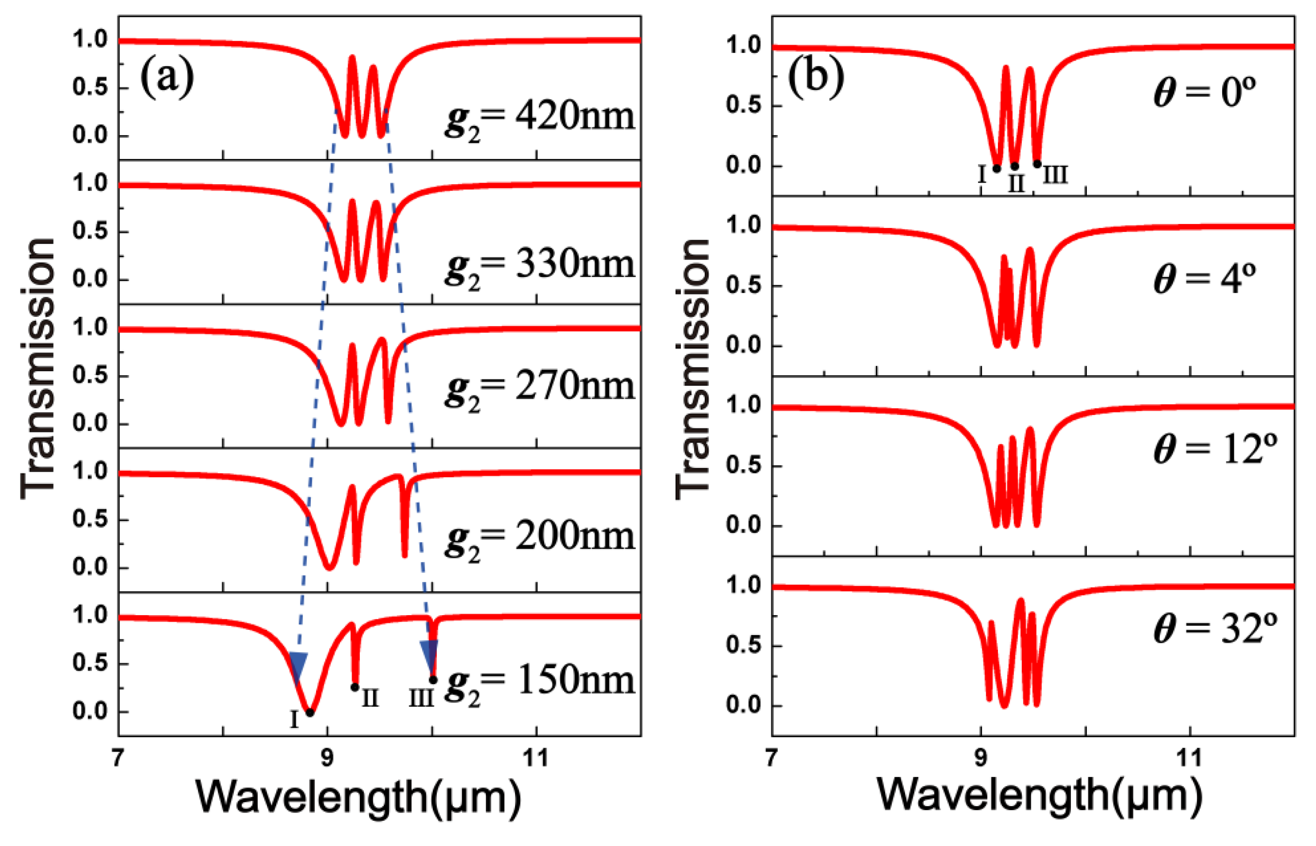
Furthermore, the second schematic of the structure employed in our design is shown in Figure 5a. The distance between the first layer of GNRs and graphene sheet layers is g. The first and the second layers of GNRs are separated by the gap g2. In one period, the two graphene nanoribbons are on the same symmetry axis. Their widths are defined as w1 and w2, respectively. A TM polarization (magnetic field is parallel to the y-axis) monochromatic plane wave comes normally from the upper surface of structure II. The transmission spectra of the structure are shown in Figure 5b. Here, p = 600 nm, w1 = 208 nm, and EF = 0.6 eV. As the width w2 increased, we can see a gradual red-shift of dip I. Especially, while w2 = 218 nm, double PIT peaks can be obtained.
In addition, the transmission spectra of structure II that we calculated at different gap g2 values are plotted in Figure 6a. As can be clearly observed, dip I is blue-shifting, whereas dip II is red-shifting as g2 shrinks. When g2 = 330 nm, double PIT peaks can be observed. While g = 330 nm keeps invariable, the angular-dependent transmission spectra of structure II are plotted in Figure 6b. With the angle of incidence increasing, dip II splits into two notches, with one blue-shifted and the other red-shifted and triple PIT peaks can be achieved.
4. Conclusions
We studied the radiative properties of graphene nanostructures by numerical simulations. Periodic graphene strips can serve as the bright element; a graphene sheet parallel to the periodic graphene strips can serve as the dark element. A graphene PIT structure can be constructed by combining the bright element with the dark element; it shows a PIT spectrum similar to the atomic EIT. Significantly, changing the gate voltage can directly tune the PIT spectrum. The position of the transmission notch greatly depends on the changes of the coupling distance and the widths of GNRs. With the appropriate distance and widths, double PIT peaks can be obtained. In addition, multiple PIT peaks can be achieved by changing the angle of incidence. Our study indicates that the demonstrated PIT devices based on graphene plasmonics may pave a new way for the development of plasmonic sensors in nanophotonics applications.
Acknowledgments
This work is supported by the National Natural Science Foundation of China (Grant No. 11504139, 11504140, 41675154, 61675185), the Natural Science Foundation of Jiangsu Province (Grant No. BK20140167). Specially, Shubin Yan thanks the Fund Program for the Natural Science Foundation of Shanxi Province (Grant No. 201601D011008), the Fund Program for the Scientific Activities of Selected Returned Overseas Professionals in Shanxi Province, the Program for the Top Youngand Middle-aged Innovative Talents of Higher Learning Institutions of Shanxi, and the North University of China Science Fund for Distinguished Young Scholars.
Author Contributions
Chunyu Lu and Jicheng Wang conceived and designed the simulation; Chunyu Lu and Liu Yang performed the simulation and analyzed the data; Chunyu Lu, Jicheng Wang and Gaige Zheng wrote the manuscript under the supervision of Jicheng Wang and Zheng-Da Hu; Jicheng Wang, Shubin Yan and Gaige Zheng supervised the project. All authors contributed to the scientific discussion of the results and reviewed the manuscript.
Conflicts of Interest
The authors declare no conflict of interest.
References
- Harris, S.E. Electromagnetically induced transparency. Phys. Today 1997, 50, 36–42. [Google Scholar] [CrossRef]
- Gu, J.Q.; Singh, R.; Liu, X.; Zhang, X.; Ma, Y.; Zhang, S.; Maier, S.A.; Tian, Z.; Azad, A.K.; Chen, H.-T.; et al. Active control of electromagnetically induced transparency analogue in terahertz metamaterials. Nat. Commun. 2012, 3, 1151. [Google Scholar] [CrossRef] [PubMed]
- Tassin, P.; Zhang, L.; Zhao, R.; Jain, A.; Koschny, T.; Soukoulis, C.M. Electromagnetically induced transparency and absorption in metamaterials: The radiating two-oscillator model and its experimental confirmation. Phys. Rev. Lett. 2012, 109, 187401. [Google Scholar] [CrossRef] [PubMed]
- Boller, K.J.; Imamoğlu, A.; Harris, S.E. Observation of electromagnetically induced transparency. Phys. Rev. Lett. 1991, 66, 2593–2596. [Google Scholar] [CrossRef] [PubMed]
- Fleischhauer, M.; Imamoglu, A.; Marangos, J.P. Electromagnetically induced transparency: Optics in coherent media. Rev. Mod. Phys. 2005, 77, 633–673. [Google Scholar] [CrossRef]
- Xu, Q.F.; Sandhu, S.; Povinelli, M.L.; Shakya, J.; Fan, S.; Lipson, M. Experimental realization of an on-chip all-optical analogue to electromagnetically induced transparency. Phys. Rev. Lett. 2006, 96, 123901. [Google Scholar] [CrossRef] [PubMed]
- Papasimakis, N.; Fedotov, V.A.; Zheludev, N.I.; Prosvirnin, S.L. Metamaterial analog of electromagnetically induced transparency. Phys. Rev. Lett. 2008, 101, 253903. [Google Scholar] [CrossRef] [PubMed]
- Zhang, S.; Genov, D.A.; Wang, Y.; Liu, M.; Zhang, X. Plasmon-induced transparency in metamaterials. Phys. Rev. Lett. 2008, 101, 047401. [Google Scholar] [CrossRef] [PubMed]
- Yang, X.D.; Yu, M.; Kwong, D.-L.; Wong, C.W. All-optical analog to electromagnetically induced transparency in multiple coupled photonic crystal cavities. Phys. Rev. Lett. 2009, 102, 173902. [Google Scholar] [CrossRef] [PubMed]
- Tassin, P.; Zhang, L.; Koschny, T.; Economou, E.N.; Soukoulis, C.M. Low-loss metamaterials based on classical electromagnetically induced transparency. Phys. Rev. Lett. 2009, 102, 053901. [Google Scholar] [CrossRef] [PubMed]
- Sun, Y.; Jiang, H.; Yang, Y.; Zhang, Y.; Chen, H.; Zhu, S. Electromagnetically induced transparency in metamaterials: Influence of intrinsic loss and dynamic evolution. Phys. Rev. B. 2011, 83, 195140. [Google Scholar] [CrossRef]
- Wright, A.R.; Xu, X.G.; Cao, J.C.; Zhang, C. Strong nonlinear optical response of graphene in the terahertz regime. Appl. Phys. Lett. 2009, 95, 072101. [Google Scholar] [CrossRef]
- Bolotin, K.I.; Sikes, K.J.; Jiang, Z.; Klima, M.; Fudenberg, G.; Hone, J.; Kim, P.; Stormer, H.L. Ultrahigh electron mobility in suspended graphene. Solid State Commun. 2008, 146, 351–355. [Google Scholar] [CrossRef]
- Balandin, A.A.; Ghosh, S.; Bao, W.; Calizo, I.; Teweldebrhan, D.; Miao, F.; Lau, C.N. Superior thermal conductivity of single-layer graphene. Nano Lett. 2008, 8, 902–907. [Google Scholar] [CrossRef] [PubMed]
- Bao, Q.L.; Loh, K.P. Graphene photonics, plasmonics, and broadband optoelectronic devices. ACS Nano 2012, 6, 3677–3694. [Google Scholar] [CrossRef] [PubMed]
- Grigorenko, A.N.; Polini, M.; Novoselov, K.S. Graphene plasmonics. Nat. Photonics 2012, 6, 749–758. [Google Scholar] [CrossRef]
- Wang, X.S.; Chen, C.; Pan, L.; Wang, J. A graphene-based Fabry-Pérot spectrometer in mid-infrared region. Sci. Rep. UK 2016, 6, 32616. [Google Scholar] [CrossRef] [PubMed]
- Song, C.; Xia, X.; Hu, Z.; Liang, Y.; Wang, J. Characteristics of plasmonic Bragg reflectors with graphene-based silicon grating. Nanoscale Res. Lett. 2016, 11, 419. [Google Scholar] [CrossRef] [PubMed]
- Li, Z.B.; Yao, K.; Xia, F.; Shen, S.; Tian, J.; Liu, Y. Graphene plasmonic metasurfaces to steer infrared light. Sci. Rep. UK 2015, 5, 12423. [Google Scholar] [CrossRef] [PubMed]
- Brar, V.W.; Jang, M.S.; Sherrott, M.; Lope, J.J.; Atwater, H.A. Highly confined tunable mid-infrared plasmonics in graphene nanoresonators. Nano Lett. 2013, 13, 2541–2547. [Google Scholar] [CrossRef] [PubMed]
- Yao, G.; Ling, F.; Yue, J.; Luo, C.; Luo, Q.; Yao, J. Dynamically electrically tunable broadband absorber based on graphene analog of electromagnetically induced transparency. IEEE Photonics J. 2016, 8, 1–8. [Google Scholar] [CrossRef]
- Li, Y.; Yu, H.; Dai, T.; Jiang, J.; Wang, G.; Yang, L.; Wang, W.; Yang, J.; Jiang, X. Graphene-based floating-gate nonvolatile optical switch. IEEE Photonics Technol. Lett. 2016, 28, 284–287. [Google Scholar] [CrossRef]
- Fahad, M.S.; Srivastava, A.; Sharma, A.K.; Mayberry, C. Analytical current transport modeling of graphene nanoribbon tunnel field-effect transistors for digital circuit design. IEEE Trans. Nanotechnol. 2016, 15, 39–50. [Google Scholar] [CrossRef]
- Yurchenko, S.O.; Komarov, K.A.; Pustovoit, V.I. Multilayer-graphene-based amplifier of surface acoustic waves. AIP Adv. 2015, 5, 057144. [Google Scholar] [CrossRef]
- Al-Dirini, F.; Mohammed, M.A.; Hossain, F.M.; Nirmalathas, T.; Skafidas, E. All-graphene planar double-quantum-dot resonant tunneling diodes. IEEE J. Electron Devices Soc. 2016, 4, 30–39. [Google Scholar] [CrossRef]
- Wang, X.C.; Zhao, W.S.; Hu, J.; Yin, W.Y. Reconfigurable terahertz leaky-wave antenna using graphene-based high-impedance surface. IEEE T. Nanotechnol. 2015, 14, 62–69. [Google Scholar] [CrossRef]
- Correas-Serrano, D.; Gomez-Diaz, J.S.; Perruisseau-Carrier, J.; Alvarez-Melcon, A. Graphene-based plasmonic tunable low-pass filters in the terahertz band. IEEE Trans. Nanotechnol. 2014, 13, 1145–1153. [Google Scholar] [CrossRef]
- Mao, X.; Cheng, C.; Huang, B.; Zhang, Z.; Gan, S.; Chen, H.; Chen, H. Optoelectronic mixer based on graphene FET. IEEE Electr. Device Soc. 2015, 36, 253–255. [Google Scholar] [CrossRef]
- Wang, Y.; Chen, Q.; Shen, X. Actively controlled plasmonic Bragg reflector based on a graphene parallel-plate waveguide. AIP Adv. 2015, 5, 1–7. [Google Scholar] [CrossRef]
- Shi, X.; Han, D.; Dai, Y.; Yu, Z.; Sun, Y.; Chen, H.; Liu, X.; Zi, J. Plasmonic analog of electromagnetically induced transparency in nanostructure graphene. Opt. Express 2013, 21, 28438–28443. [Google Scholar] [CrossRef] [PubMed]
- Hanson, G.W. Quasi-transverse electromagnetic modes supported by a graphene parallel-plate waveguide. J. Appl. Phys. 2008, 104, 084314. [Google Scholar] [CrossRef]
- Li, H.J.; Wang, L.L.; Sun, B.; Huang, Z.R.; Zhai, X. Controlling mid-infrared surface plasmon polaritons in the parallel graphene pair. Appl. Phys. Express 2014, 7, 125101. [Google Scholar] [CrossRef]
- Wang, L.; Li, W.; Jiang, X.Y. Tunable control of electromagnetically induced transparency analogue in a compact graphene-based waveguide. Opt. Lett. 2015, 40, 2325–2328. [Google Scholar] [CrossRef] [PubMed]
- Lin, Q.; Zhai, X.; Wang, L.; Wang, B.; Liu, G.; Xia, S. Combined theoretical analysis for plasmon-induced transparency in integrated graphene waveguides with direct and indirect couplings. EPL Europhys. Lett. 2015, 111, 34004. [Google Scholar] [CrossRef]
- Wang, B.; Zhang, X.; Yuan, X.; Teng, J. Optical coupling of surface plasmons between graphene sheets. Appl. Phys. Lett. 2012, 100, 131111. [Google Scholar] [CrossRef]
- Jablan, M.; Buljan, H.; Soljacic, M. Plasmonics in graphene at infrared frequencies. Phys. Rev. B 2009, 80, 245435. [Google Scholar] [CrossRef]
- Lu, Y.; Xu, H.; Rhee, J.Y.; Jang, W.H.; Ham, B.S.; Lee, Y. Magnetic plasmon resonance: Underlying route to plasmonic electromagnetically induced transparency in metamaterials. Phys. Rev. B 2010, 82, 195112. [Google Scholar] [CrossRef]
Figure 1.
(a) First schematic of the proposed structure. The graphene nanoribbons (GNRs) are lying periodically above an infinite-width graphene sheet and p represents the cycle of the unit element. The distance between GNRs and the graphene sheet is g. The widths of the two adjacent GNRs are defined as w1 and w2, respectively; (b) Cross-sectional diagram of Structure I.
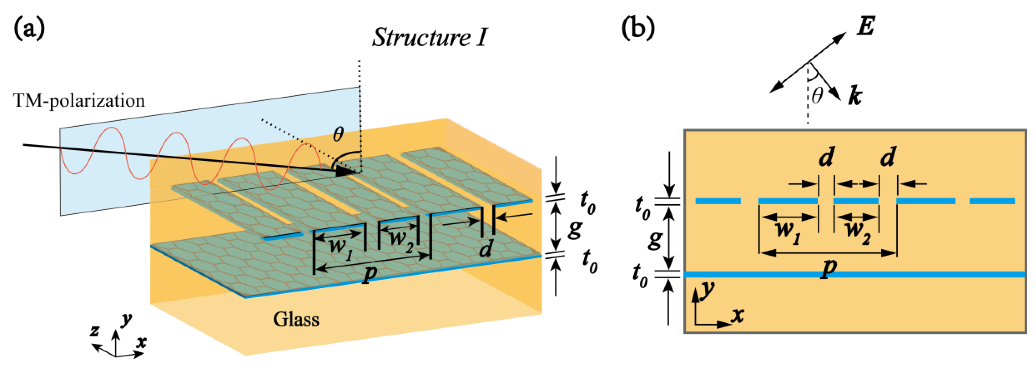
Figure 2.
(a–c) Transmission and reflection spectra for the basic unit at normal incidence. The inset graphs are the diagrammatic sketch of graphene nanostructures under research. There are two graphene nanoribbons acting as the bright element. The graphene sheet layers are acting as the dark element. The basic unit of the graphene plasmonic structure aims to achieve plasmon-induced transparency (PIT). It is constructed by combining the bright element with the dark element. Blue areas represent graphene; (d) The |E| distributions corresponding to three different wavelengths; (e) Transmission spectra of the system for chemical potential EF = 0.4, 0.6, and 0.8 eV.

Figure 3.
(a,b) Computerized ionospheric tomography transmission spectra at different widths w2. Here, p = 1200 nm, w1 = 208 nm, g = 350 nm, and EF = 0.6 eV; (c–e) Field distributions Ey of the transmission dips.
Figure 3.
(a,b) Computerized ionospheric tomography transmission spectra at different widths w2. Here, p = 1200 nm, w1 = 208 nm, g = 350 nm, and EF = 0.6 eV; (c–e) Field distributions Ey of the transmission dips.

Figure 4.
(a) Transmission spectra of structure I at different gap g values between the graphene sheet and the GNRs; (b–d) The field distributions Ey of the transmission dips under g = 340 nm; (e) Spectral responses of structure I with different angles of incidence.
Figure 4.
(a) Transmission spectra of structure I at different gap g values between the graphene sheet and the GNRs; (b–d) The field distributions Ey of the transmission dips under g = 340 nm; (e) Spectral responses of structure I with different angles of incidence.
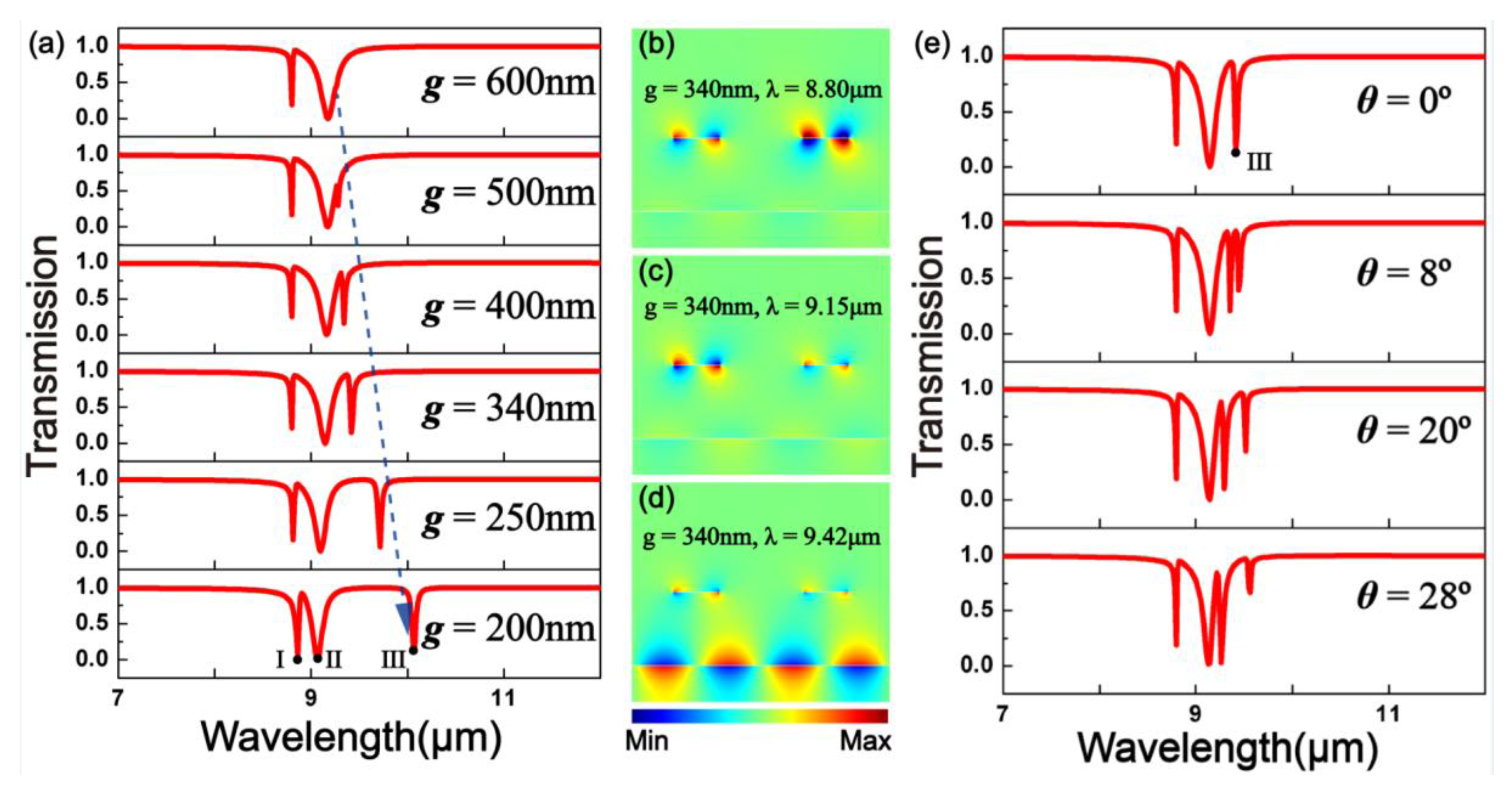
Figure 5.
(a) Cross-sectional diagram of the second structure proposed; (b) Computerized ionospheric tomography transmission spectra at different widths w2. Here, p = 600 nm, w1 = 208 nm, g = 350 nm, and EF = 0.6 eV.
Figure 5.
(a) Cross-sectional diagram of the second structure proposed; (b) Computerized ionospheric tomography transmission spectra at different widths w2. Here, p = 600 nm, w1 = 208 nm, g = 350 nm, and EF = 0.6 eV.

Figure 6.
(a) Transmission spectra of structure II at diverse gap g2 values between the first and the second layers of GNRs; (b) Spectral responses of structure II at different angles of incidence.
Figure 6.
(a) Transmission spectra of structure II at diverse gap g2 values between the first and the second layers of GNRs; (b) Spectral responses of structure II at different angles of incidence.

© 2017 by the authors. Licensee MDPI, Basel, Switzerland. This article is an open access article distributed under the terms and conditions of the Creative Commons Attribution (CC BY) license (http://creativecommons.org/licenses/by/4.0/).
Share and Cite
MDPI and ACS Style
Lu, C.; Wang, J.; Yan, S.; Hu, Z.-D.; Zheng, G.; Yang, L. Tunable Multiple Plasmon-Induced Transparencies Based on Asymmetrical Grapheme Nanoribbon Structures. Materials 2017, 10, 699. https://doi.org/10.3390/ma10070699
AMA Style
Lu C, Wang J, Yan S, Hu Z-D, Zheng G, Yang L. Tunable Multiple Plasmon-Induced Transparencies Based on Asymmetrical Grapheme Nanoribbon Structures. Materials. 2017; 10(7):699. https://doi.org/10.3390/ma10070699
Chicago/Turabian StyleLu, Chunyu, Jicheng Wang, Shubin Yan, Zheng-Da Hu, Gaige Zheng, and Liu Yang. 2017. "Tunable Multiple Plasmon-Induced Transparencies Based on Asymmetrical Grapheme Nanoribbon Structures" Materials 10, no. 7: 699. https://doi.org/10.3390/ma10070699
Note that from the first issue of 2016, this journal uses article numbers instead of page numbers. See further details here.