
Influence of Discharge Current on Phase Transition Properties of High Quality Polycrystalline VO2 Thin Film Fabricated by HiPIMS

Abstract
:
1. Introduction
2. Experimental Detail
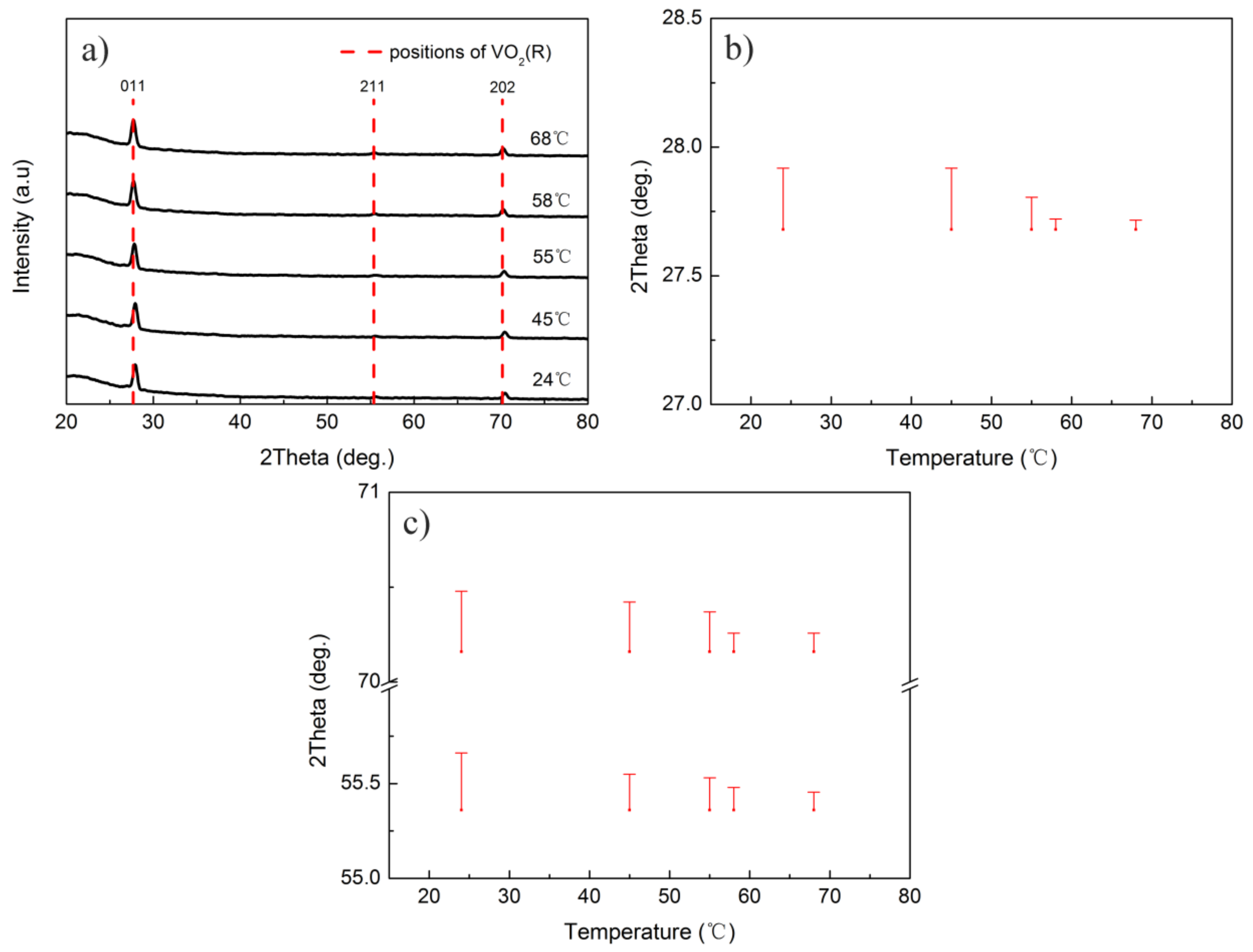
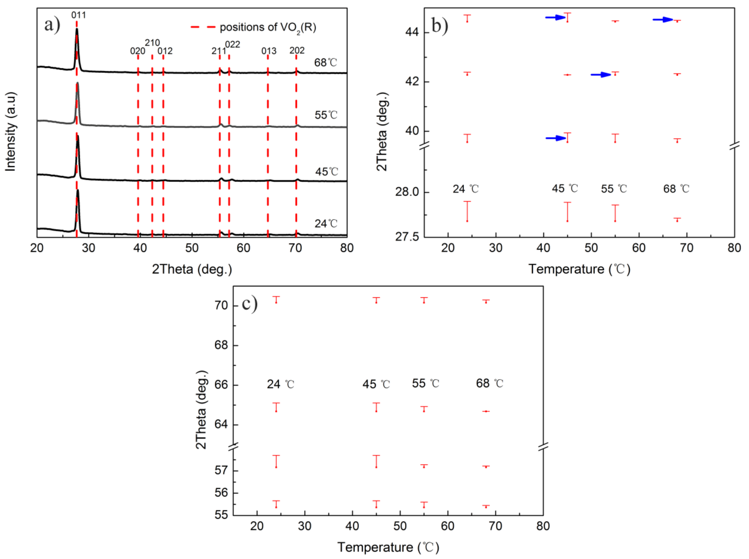
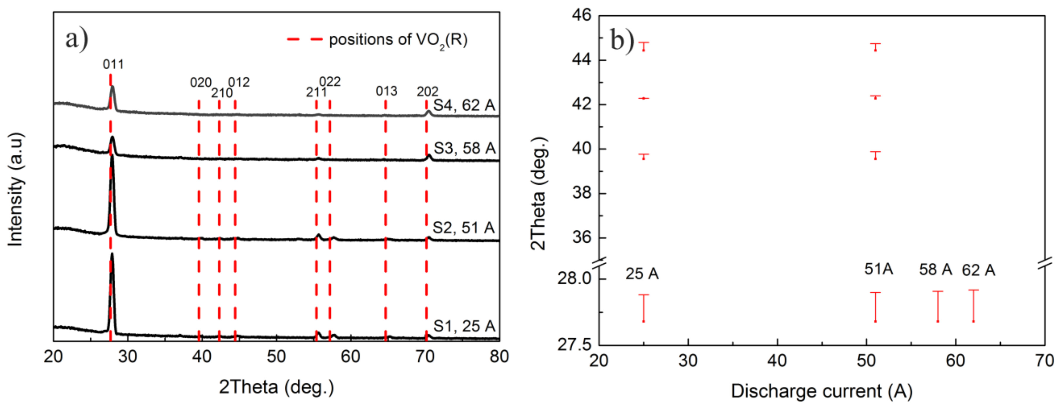
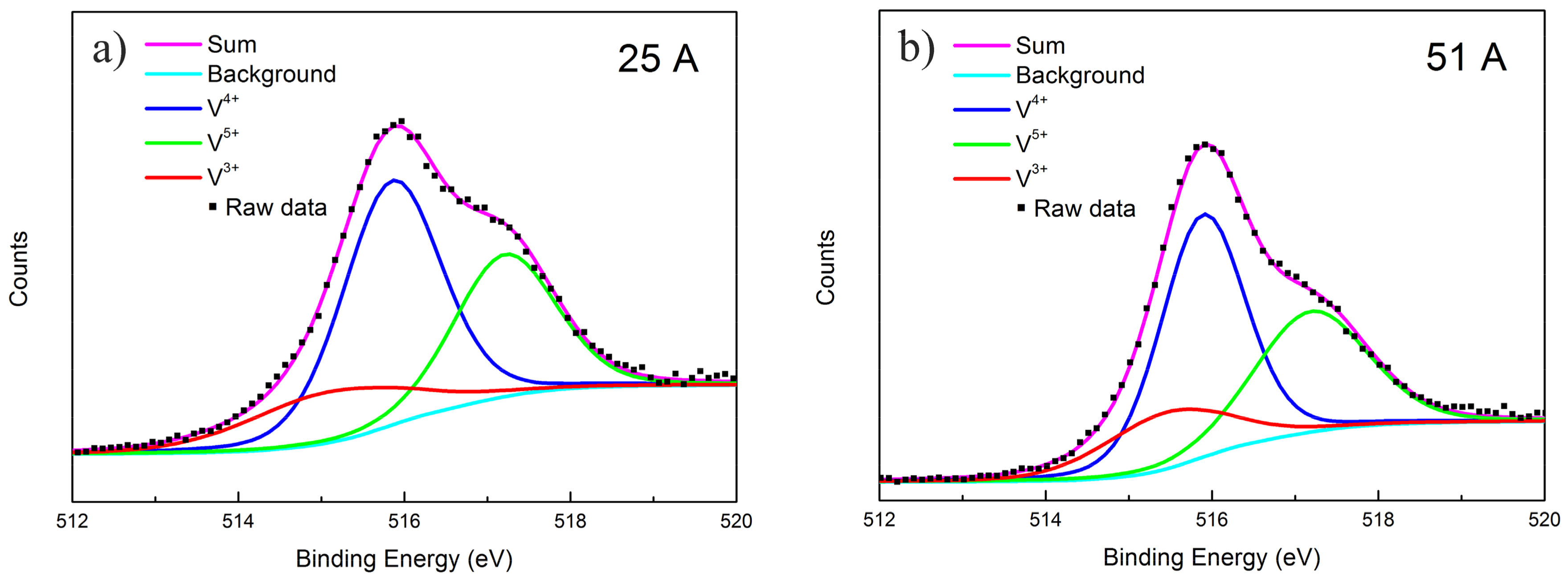
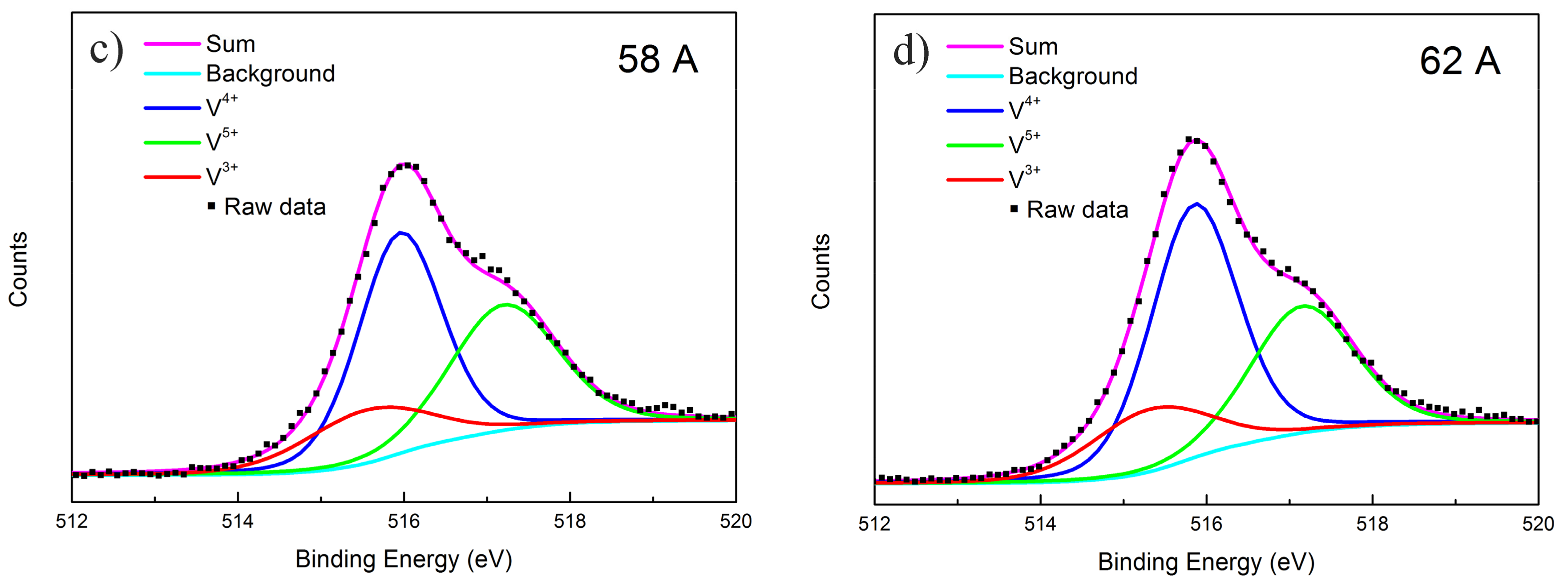
3. Results and Discussion
4. Conclusions
Acknowledgments
Author Contributions
Conflicts of Interest
References
- Kim, H.; Charipar, N.; Osofsky, M.; Qadri, S.B.; Piqué, A. Optimization of the semiconductor-metal transition in VO2 epitaxial thin films as a function of oxygen growth pressure. Appl. Phys. Lett. 2014, 104, 081913. [Google Scholar] [CrossRef]
- Morrison, V.R.; Chatelain, R.P.; Tiwari, K.L.; Hendaoui, A.; Bruhacs, A.; Chaker, M.; Siwick, B.J. A photoinduced metal-like phase of monoclinic VO2 revealed by ultrafast electron diffraction. Science 2014, 346, 445–448. [Google Scholar] [CrossRef] [PubMed]
- Sun, G.; Zhou, H.; Cao, X.; Li, R.; Tazawa, M.; Okada, M.; Jin, P. Self-Assembled Multilayer Structure and Enhanced Thermochromic Performance of Spinodally Decomposed TiO2-VO2 Thin Film. ACS Appl. Mater. Interfaces 2016, 8, 7054–7059. [Google Scholar] [CrossRef] [PubMed]
- Ji, Y.; Zhang, Y.; Gao, M.; Yuan, Z.; Xia, Y.; Jin, C.; Tao, B.; Chen, C.; Jia, Q. Role of microstructures on the M1-M2 phase transition in epitaxial VO2 thin films. Sci. Rep. 2014, 4, 4854. [Google Scholar] [CrossRef] [PubMed]
- Yoon, J.; Lee, G.; Park, C.; Mun, B.S.; Ju, H. Investigation of length-dependent characteristics of the voltage-induced metal insulator transition in VO2 film devices. Appl. Phys. Lett. 2014, 105, 083503. [Google Scholar] [CrossRef]
- Kumar, S.; Strachan, J.P.; Pickett, M.D.; Bratkovsky, A.; Nishi, Y.; Williams, R.S. Sequential electronic and structural transitions in VO2 observed using X-ray absorption spectromicroscopy. Adv. Mater. 2014, 26, 7505–7509. [Google Scholar] [CrossRef] [PubMed]
- Brassard, D.; Fourmaux, S.; Jean-Jacques, M.; Kieffer, J.C.; El Khakani, M.A. Grain size effect on the semiconductor-metal phase transition characteristics of magnetron-sputtered VO2 thin films. Appl. Phys. Lett. 2005, 87, 051910. [Google Scholar] [CrossRef]
- Mlyuka, N.R.; Niklasson, G.A.; Granqvist, C.G. Thermochromic multilayer films of VO2 and TiO2 with enhanced transmittance. Sol. Energy Mater. Sol. Cells 2009, 93, 1685–1687. [Google Scholar] [CrossRef]
- Romanyuk, A.; Steiner, R.; Marot, L.; Spassov, V.; Oelhafen, P. nc-VO2/Al2O3 nanocomposite films prepared by dual target magnetron sputtering. Thin Solid Films 2008, 516, 8513–8516. [Google Scholar] [CrossRef]
- Azhan, N.H.; Su, K.; Okimura, K.; Sakai, J. Radio frequency substrate biasing effects on the insulator-metal transition behavior of reactively sputtered VO2 films on sapphire (001). J. Appl. Phys. 2015, 117, 185307. [Google Scholar] [CrossRef]
- Chen, S.; Lai, J.; Dai, J.; Ma, H.; Wang, H.; Yi, X. Characterization of nanostructured VO2 thin films grown by magnetron controlled sputtering deposition and post annealing method. Opt. Express 2009, 17, 24153–24161. [Google Scholar] [CrossRef] [PubMed]
- Fu, G.; Polity, A.; Volbers, N.; Meyer, B.K. Annealing effects on VO2 thin films deposited by reactive sputtering. Thin Solid Films 2006, 515, 2519–2522. [Google Scholar] [CrossRef]
- Peter, A.P.; Martens, K.; Rampelberg, G.; Toeller, M.; Ablett, J.M.; Meersschaut, J.; Cuypers, D.; Ranquet, A.; Detavernier, C.; Rueff, J. Metal–Insulator Transition in ALD VO2 Ultrathin Films and Nanoparticles: Morphological Control. Adv. Funct. Mater. 2015, 25, 679–686. [Google Scholar] [CrossRef]
- Skuza, J.R.; Scott, D.W.; Pradhan, A.K. Sapphire substrate-induced effects in VO2 thin films grown by oxygen plasma-assisted pulsed laser deposition. J. Appl. Phys. 2015, 118, 195303. [Google Scholar] [CrossRef]
- Bayati, M.R.; Molaei, R.; Wu, F.; Budai, J.D.; Liu, Y.; Narayan, R.J.; Narayan, J. Correlation between structure and semiconductor-to-metal transition characteristics of VO2/TiO2/sapphire thin film heterostructures. Acta Mater. 2013, 61, 7805–7815. [Google Scholar] [CrossRef]
- Chen, F.H.; Fan, L.L.; Chen, S.; Liao, G.M.; Chen, Y.L.; Wu, P.; Song, L.; Zou, C.W.; Wu, Z.Y. Control of the metal–insulator transition in VO2 epitaxial film by modifying carrier density. ACS Appl. Mater. Interfaces 2015, 7, 6875–6881. [Google Scholar] [CrossRef] [PubMed]
- Guo, Y.; Xu, H.; Zou, C.; Yang, Z.; Tong, B.; Yu, J.; Zhang, Y.; Zhao, L.; Wang, Y. Evolution of structure and electrical properties with annealing time in solution-based VO2 thin films. J. Alloys Compd. 2015, 622, 913–917. [Google Scholar] [CrossRef]
- He, X.; Xu, J.; Xu, X.; Gu, C.; Chen, F.; Wu, B.; Wang, C.; Xing, H.; Chen, X.; Chu, J. Negative capacitance switching via VO2 band gap engineering driven by electric field. Appl. Phys. Lett. 2015, 106, 093106. [Google Scholar] [CrossRef]
- Ji, Y.-X.; Niklasson, G.A.; Granqvist, C.G.; Boman, M. Thermochromic VO2 films by thermal oxidation of vanadium in SO2. Sol. Energy Mater. Sol. Cells 2016, 144, 713–716. [Google Scholar] [CrossRef]
- Leroy, J.; Bessaudou, A.; Cosset, F.; Crunteanu, A. Structural, electrical and optical properties of thermochromic VO2 thin films obtained by reactive electron beam evaporation. Thin Solid Films 2012, 520, 4823–4825. [Google Scholar] [CrossRef]
- Jeong, J.; Aetukuri, N.; Graf, T.; Schladt, T.D.; Samant, M.G.; Parkin, S.S. Suppression of metal–insulator transition in VO2 by electric field-induced oxygen vacancy formation. Science 2013, 339, 1402–1405. [Google Scholar] [CrossRef] [PubMed]
- Kana, J.B.K.; Ndjaka, J.M.; Ateba, P.O.; Ngom, B.D.; Manyala, N.; Nemraoui, O.; Beye, A.C.; Maaza, M. Thermochromic VO2 thin films synthesized by rf-inverted cylindrical magnetron sputtering. Appl. Surf. Sci. 2008, 254, 3959–3963. [Google Scholar] [CrossRef]
- Miller, M.J.; Wang, J. Influence of grain size on transition temperature of thermochromic VO2. J. Appl. Phys. 2015, 117, 034307. [Google Scholar] [CrossRef]
- Fortier, J.P.; Baloukas, B.; Zabeida, O.; Klemberg-Sapieha, J.E.; Martinu, L. Thermochromic VO2 thin films deposited by HiPIMS. Sol. Energy Mater. Sol. Cells 2014, 125, 291–296. [Google Scholar] [CrossRef]
- Yu, Q.; Li, W.; Liang, J.; Duan, Z.; Hu, Z.; Liu, J.; Chen, H.; Chu, J. Oxygen pressure manipulations on the metal–insulator transition characteristics of highly (011)-oriented vanadium dioxide films grown by magnetron sputtering. J. Phys. D Appl. Phys. 2013, 46, 055310. [Google Scholar] [CrossRef]
- Jian, J.; Zhang, W.; Jacob, C.; Chen, A.; Wang, H.; Huang, J.; Wang, H. Roles of grain boundaries on the semiconductor to metal phase transition of VO2 thin films. Appl. Phys. Lett. 2015, 107, 102105. [Google Scholar] [CrossRef]
- Zhang, D.-P.; Zhu, M.-D.; Liu, Y.; Yang, K.; Liang, G.-X.; Zheng, Z.-H.; Cai, X.-M.; Fan, P. High performance VO2 thin films growth by DC magnetron sputtering at low temperature for smart energy efficient window application. J. Alloys Compd. 2016, 659, 198–202. [Google Scholar] [CrossRef]
- Ba, C.; Bah, S.T.; D’Auteuil, M.; Ashrit, P.V.; Vallee, R. Fabrication of high-quality VO2 thin films by ion-assisted dual ac magnetron sputtering. ACS Appl. Mater. Interfaces 2013, 5, 12520–12525. [Google Scholar] [CrossRef] [PubMed]
- Muraoka, Y.; Hiroi, Z. Metal–insulator transition of VO2 thin films grown on TiO2 (001) and (110) substrates. Appl. Phys. Lett. 2002, 80, 583. [Google Scholar] [CrossRef]
- Liu, X.; Wang, S.-W.; Chen, F.; Yu, L.; Chen, X. Tuning phase transition temperature of VO2 thin films by annealing atmosphere. J. Phys. D Appl. Phys. 2015, 48, 265104. [Google Scholar] [CrossRef]
- Mlyuka, N.R.; Niklasson, G.A.; Granqvist, C.G. Mg doping of thermochromic VO2 films enhances the optical transmittance and decreases the metal–insulator transition temperature. Appl. Phys. Lett. 2009, 95, 171909. [Google Scholar] [CrossRef]
- Azhan, N.H.; Okimura, K.; Ohtsubo, Y.; Kimura, S.-I.; Zaghrioui, M.; Sakai, J. Large modification in insulator-metal transition of VO2 films grown on Al2O3 (001) by high energy ion irradiation in biased reactive sputtering. J. Appl. Phys. 2016, 119, 055308. [Google Scholar] [CrossRef]
- Lin, T.; Wang, L.; Wang, X.; Zhang, Y.; Yu, Y. Influence of lattice distortion on phase transition properties of polycrystalline VO2 thin film. Appl. Surf. Sci. 2016, 379, 179–185. [Google Scholar] [CrossRef]
- Lin, T.; Wang, L.; Wang, X.; Zhang, Y. Characterization of polycrystalline VO2 thin film with low phase transition temperature fabricated by high power impulse magnetron sputtering. Funct. Mater. Lett. 2016, 9, 1650033. [Google Scholar] [CrossRef]
- Agnarsson, B.; Magnus, F.; Tryggvason, T.K.; Ingason, A.S.; Leosson, K.; Olafsson, S.; Gudmundsson, J.T. Rutile TiO2 thin films grown by reactive high power impulse magnetron sputtering. Thin Solid Films 2013, 545, 445–450. [Google Scholar] [CrossRef]
- Kouznetsov, V.; Macak, K.; Schneider, J.M.; Helmersson, U.; Petrov, I. A novel pulsed magnetron sputter technique utilizing very high target power densities. Surf. Coat. Technol. 1999, 122, 290–293. [Google Scholar] [CrossRef]
- Stranak, V.; Quaas, M.; Bogdanowicz, R.; Steffen, H.; Wulff, H.; Hubicka, Z.; Tichy, M.; Hippler, R. Effect of nitrogen doping on TiOxNy thin film formation at reactive high-power pulsed magnetron sputtering. J. Phys. D Appl. Phys. 2010, 43, 285203. [Google Scholar] [CrossRef]
- Anders, A. Discharge physics of high power impulse magnetron sputtering. Surf. Coat. Technol. 2011, 205, S1–S9. [Google Scholar] [CrossRef]
- Sarakinos, K.; Alami, J.; Konstantinidis, S. High power pulsed magnetron sputtering: A review on scientific and engineering state of the art. Surf. Coat. Technol. 2010, 204, 1661–1684. [Google Scholar] [CrossRef]
- Chen, R.; Miao, L.; Liu, C.; Zhou, J.; Cheng, H.; Asaka, T.; Iwamoto, Y.; Tanemura, S. Shape-controlled synthesis and influence of W doping and oxygen nonstoichiometry on the phase transition of VO2. Sci. Rep. 2015, 5, 14087. [Google Scholar] [CrossRef] [PubMed]
- Zhang, Z.; Gao, Y.; Chen, Z.; Du, J.; Cao, C.; Kang, L.; Luo, H. Thermochromic VO2 thin films: Solution-based processing, improved optical properties, and lowered phase transformation temperature. Langmuir ACS J. Surf. Colloids 2010, 26, 10738–10744. [Google Scholar] [CrossRef] [PubMed]
- Yang, T.-H.; Nori, S.; Mal, S.; Narayan, J. Control of room-temperature defect-mediated ferromagnetism in VO2 films. Acta Mater. 2011, 59, 6362–6368. [Google Scholar] [CrossRef]
- Dou, Y.-K.; Li, J.-B.; Cao, M.-S.; Su, D.-Z.; Rehman, F.; Zhang, J.-S.; Jin, H.-B. Oxidizing annealing effects on VO2 films with different microstructures. Appl. Surf. Sci. 2015, 345, 232–237. [Google Scholar] [CrossRef]
- Émond, N.; Hendaoui, A.; Ibrahim, A.; Al-Naib, I.; Ozaki, T.; Chaker, M. Transmission of reactive pulsed laser deposited VO2 films in the THz domain. Appl. Surf. Sci. 2016, 379, 377–383. [Google Scholar] [CrossRef]


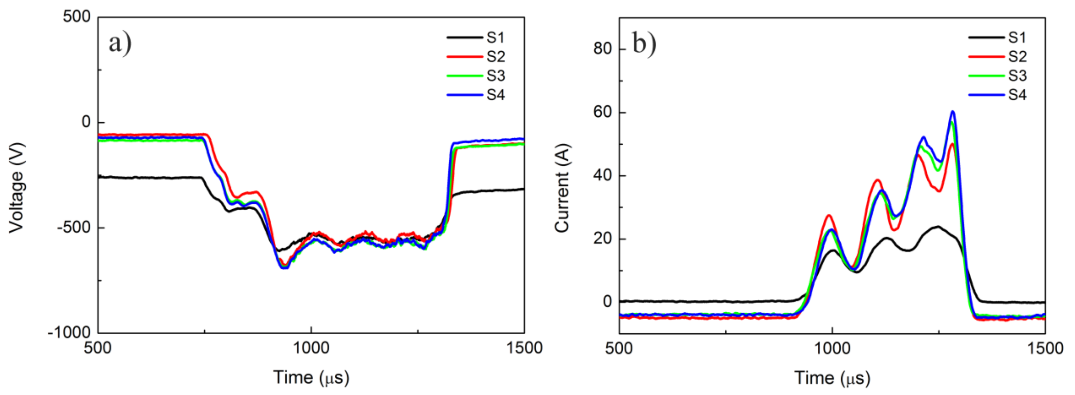
| Sample No. | Discharge Voltage (V) | Peak Current (A) | Pulse Frequency (Hz) | Pulse Width (μs) | Average Power (W) |
|---|---|---|---|---|---|
| S1 | 640 | 25 | 100 | 400 | 403 |
| S2 | 670 | 51 | 50 | 400 | 385 |
| S3 | 680 | 58 | 50 | 400 | 401 |
| S4 | 683 | 62 | 50 | 400 | 403 |
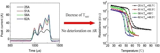
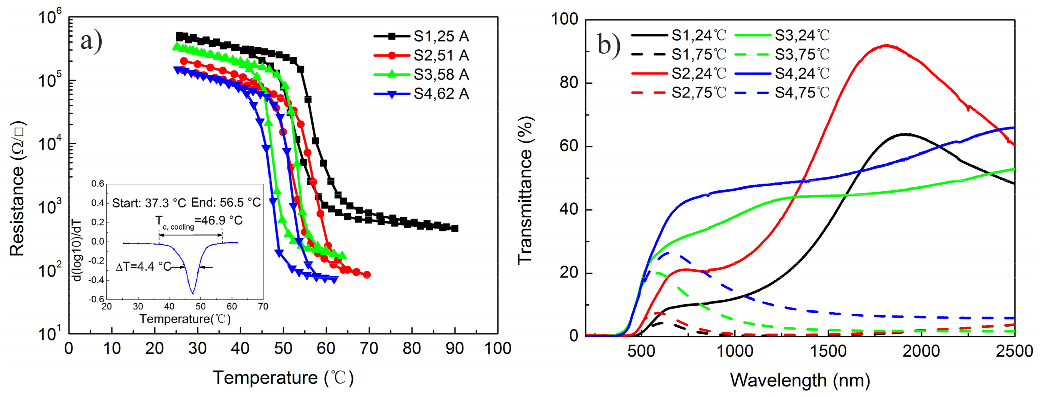
| Sample No. | Tc, heating (°C) | Tc, cooling (°C) | TMIT (°C) | ∆H (°C) | ∆T (°C) | R0 (Ω/□) | R1 (Ω/□) | ∆R |
|---|---|---|---|---|---|---|---|---|
| S1 | 58 | 53.4 | 55.7 | 4.6 | 8.5 | 5.2 × 10⁵ | 4.7 × 10² | 1.1 × 10³ |
| S2 | 55.6 | 51 | 53.3 | 4.6 | 7.4 | 2 × 10⁵ | 90 | 2.2 × 10³ |
| S3 | 52.8 | 47.2 | 50 | 5.6 | 4.6 | 3.1 × 10⁵ | 1.9 × 10² | 1.6 × 10³ |
| S4 | 51.5 | 46.9 | 49.2 | 4.6 | 4.4 | 1.5 × 10⁵ | 70 | 2.1 × 10³ |
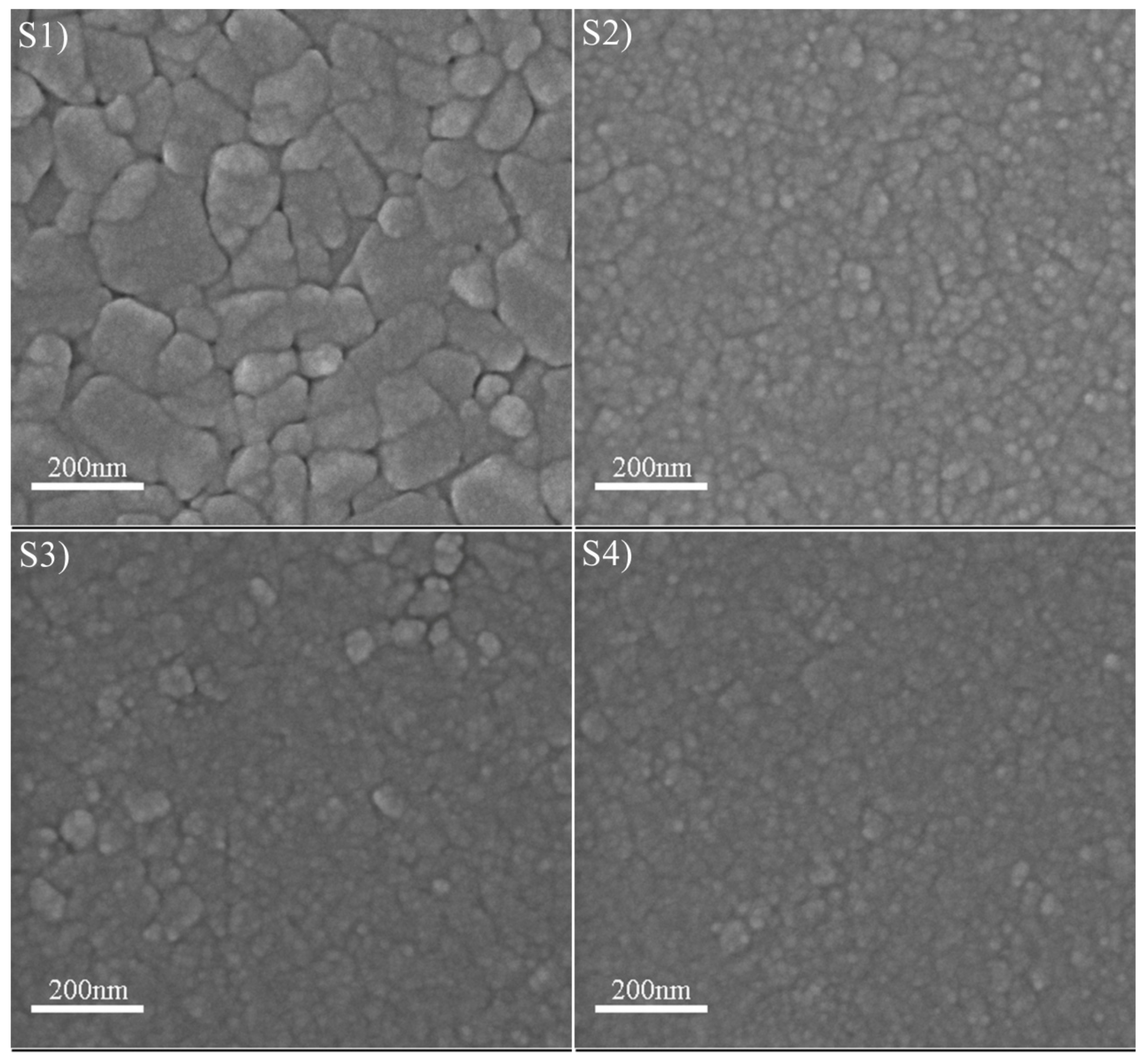
| Sample No. | V3+ | V4+ | V5+ |
|---|---|---|---|
| S1 | 17.60% | 51.38% | 31.02% |
| S2 | 17.14% | 49.69% | 33.17% |
| S3 | 17.07% | 48% | 34.93% |
| S4 | 17.30% | 51.80% | 30.90% |
© 2017 by the authors. Licensee MDPI, Basel, Switzerland. This article is an open access article distributed under the terms and conditions of the Creative Commons Attribution (CC BY) license (http://creativecommons.org/licenses/by/4.0/).
Share and Cite
Lin, T.; Wang, J.; Liu, G.; Wang, L.; Wang, X.; Zhang, Y. Influence of Discharge Current on Phase Transition Properties of High Quality Polycrystalline VO2 Thin Film Fabricated by HiPIMS. Materials 2017, 10, 633. https://doi.org/10.3390/ma10060633
Lin T, Wang J, Liu G, Wang L, Wang X, Zhang Y. Influence of Discharge Current on Phase Transition Properties of High Quality Polycrystalline VO2 Thin Film Fabricated by HiPIMS. Materials. 2017; 10(6):633. https://doi.org/10.3390/ma10060633
Chicago/Turabian StyleLin, Tiegui, Jian Wang, Gang Liu, Langping Wang, Xiaofeng Wang, and Yufen Zhang. 2017. "Influence of Discharge Current on Phase Transition Properties of High Quality Polycrystalline VO2 Thin Film Fabricated by HiPIMS" Materials 10, no. 6: 633. https://doi.org/10.3390/ma10060633