Communication

Frequency-Stable Ionic-Type Hybrid Gate Dielectrics for High Mobility Solution-Processed Metal-Oxide Thin-Film Transistors

1
School of Electrical and Electronic Engineering, Chung-Ang University, Seoul 06980, Korea
2
SKKU Advanced Institute of Nanotechnology (SAINT) and School of Advanced Materials Science and Engineering, Sungkyunkwan University, Suwon 16419, Korea
*
Authors to whom correspondence should be addressed.
Materials 2017, 10(6), 612; https://doi.org/10.3390/ma10060612
Submission received: 19 April 2017 / Revised: 27 May 2017 / Accepted: 1 June 2017 / Published: 3 June 2017
(This article belongs to the Special Issue Oxide Semiconductor Thin-Film Transistor)

Abstract

:
In this paper, we demonstrate high mobility solution-processed metal-oxide thin-film transistors (TFTs) by using a high-frequency-stable ionic-type hybrid gate dielectric (HGD). The HGD gate dielectric, a blend of sol-gel aluminum oxide (AlOx) and poly(4-vinylphenol) (PVP), exhibited high dielectric constant (ε~8.15) and high-frequency-stable characteristics (1 MHz). Using the ionic-type HGD as a gate dielectric layer, an minimal electron-double-layer (EDL) can be formed at the gate dielectric/InOx interface, enhancing the field-effect mobility of the TFTs. Particularly, using the ionic-type HGD gate dielectrics annealed at 350 °C, InOx TFTs having an average field-effect mobility of 16.1 cm2/Vs were achieved (maximum mobility of 24 cm2/Vs). Furthermore, the ionic-type HGD gate dielectrics can be processed at a low temperature of 150 °C, which may enable their applications in low-thermal-budget plastic and elastomeric substrates. In addition, we systematically studied the operational stability of the InOx TFTs using the HGD gate dielectric, and it was observed that the HGD gate dielectric effectively suppressed the negative threshold voltage shift during the negative-illumination-bias stress possibly owing to the recombination of hole carriers injected in the gate dielectric with the negatively charged ionic species in the HGD gate dielectric.

1. Introduction

Solution-processed metal-oxide thin-film transistors (TFTs) are emerging as a potential replacement for amorphous and low-temperature polycrystalline silicon TFTs in active-matrix electronics including displays, sensor arrays, and driving circuits due to their relatively high carrier mobility and good scalability over a large area [1,2,3,4]. In addition, their amorphous nature and high optical transparency in the visible range may open up a new promising application for transparent and wearable electronics. In general, the metal-oxide TFTs such as indium-gallium-zinc oxide exhibit a higher carrier mobility than that of the amorphous silicon and organic TFTs [5,6]. However, in order to realize high definition, high frame-rate displays, and the relevant driving circuitry, the carrier mobility must be further improved while exhibiting good operational stability. For these reasons, various metal-oxide semiconductors [7,8], gate dielectrics [9,10], novel device structures [11,12], and post treatments [13,14] have been proposed to enhance the carrier mobility of these devices. Among the various approaches in achieving high mobility metal-oxide TFTs, using an ionic-type gate dielectric is a promising method of achieving both the high mobility and low voltage operation characteristics [15,16,17,18,19]. Previously, ion-gel-type gate dielectrics [20], protonated SiO2 gate dielectrics [21], and electrolyte gate dielectrics have been explored. Although these ionic-type gate dielectrics showed promising results for achieving high mobility devices, their limited operation at high frequencies may hinder their practical application in active-matrix electronics. In this respect, new types of ionic-type gate dielectrics, which are capable of operating at high frequencies, are now in high demand. Moreover, for the consistency in the fabrication process of oxide TFTs, solution processing of frequency-stable ionic-type gate dielectrics will be more favorable.
Here, we demonstrate solution-processed ionic-type gate dielectrics based on AlOx and a hybrid of AlOx and poly(4-vinylphenol) (PVP) materials. In particularly, the low-temperature solution-processed hybrid gate dielectric (HGD) exhibited reasonably high capacitance and dielectric constant, and only a slight decrease in areal capacitance was observed at high frequencies up to 1 MHz along with minimal hysteresis due to the local confinement of mobile ions inside the polymer networks and consequent suppression of electron-double-layer (EDL) effects [22]. In addition, using the solution-processed HGD gate dielectrics in indium oxide (InOx) TFTs, relatively high mobilities up to 24 cm2/Vs were achieved due to the formation of an acceptable EDL at the gate dielectric/InOx interface for high frequency applications. These results demonstrate that the low-temperature solution-processed HGD gate dielectrics may enable the high-mobility, low-voltage, and high-frequency operation of oxide TFTs.

2. Experimental Procedure

For the fabrication of an AlOx gate dielectric, an AlOx precursor solution was prepared by dissolving 0.8 M aluminum nitrate nonahydrate in 2-methoxyethanol (2-ME) followed by vigorously stirring at 75 °C for 12 h. For the HGD gate dielectric, a poly(4-vinylphenol) (PVP) precursor was dissolved by stirring in 2-ME for 12 h to form a 5 mg mL−1 solution. Then, an additional 5% PVP (AlOx: 5% PVP) was added to the AlOx precursor solution and stirred for 6 h at 75 °C. For the InOx channel formation by a solution process, 0.1 M indium nitrate was dissolved in 2-ME and stirred for 12 h at 75 °C. For the electrical characterization of solution-processed gate dielectrics, a heavily-doped n+ Si wafer was used as a substrate, and Si wafer/AlOx(or HGD)/Al (metal-insulator-metal; MIM) and Si wafer/AlOx(or HGD)/InOx/Al (metal-insulator-semiconductor; MIS) structures were constructed. The top Al was deposited by using a thermal evaporator with a shadow mask (effective area: 100 × 100 μm2). For the fabrication of InOx TFTs, a borosilicate glass was used as a substrate. Then, Cr gate electrode was deposited by e-beam evaporation and patterned by using standard photolithography and wet etching processes. Afterwards, the AlOx or HGD precursor solution was spin-coated over the gate electrode to form a gate dielectric layer. Thermal annealing treatment at 150, 250, 350, and 450 °C for 30 min was carried out in an ambient air condition, resulting in thicknesses of 89, 60, 50 and 40 nm, respectively. After the formation of the gate dielectric, an InOx precursor solution was spin-coated to form a channel layer and thermally annealed at 250 °C for 30 min, resulting in a thickness of 7 nm. For the source/drain electrodes, 60-nm-thick indium zinc oxide (IZO) was deposited by sputtering and patterned by a lift-off process (Figure 1a). The channel width and length of the InOx TFTs were 100 μm and 10 μm, respectively. The thickness of the gate dielectric layer was measured by using spectroscopic ellipsometry, and to obtain the dielectric constant (εr) of the film, the capacitance value (C) was first assessed by using a precision LCR meter and the dielectric constant was extracted using the following equation:
C = ε 0 ε r A d
where C is the capacitance, A is the overlapped area between top and bottom electrodes, d is the thickness of gate dielectric layer, and ε0 is the vacuum permittivity, respectively.
To evaluate the dielectric properties of AlOx and HGD films, areal capacitance vs. frequency and leakage current density vs. electric field were analyzed using a precision LCR meter and a semiconductor parameter analyzer, respectively. In addition, the electrical characterization and bias stability tests for the InOx TFTs were carried out using a semiconductor parameter analyzer under an ambient air condition with a relative humidity of ~33% and a temperature of 24 °C. For analyzing the transfer characteristics, the gate voltage was swept from −5 to 6 V with a voltage step of 0.1 V. Additionally, it should be noted that, since the degree of hysteresis in the transfer curves and the field-effect mobility of InOx TFTs with low-temperature annealed gate dielectric can vary with the gate-voltage sweep rate, we applied a gate-voltage sweep rate of 0.13 V/s for all TFT measurement.

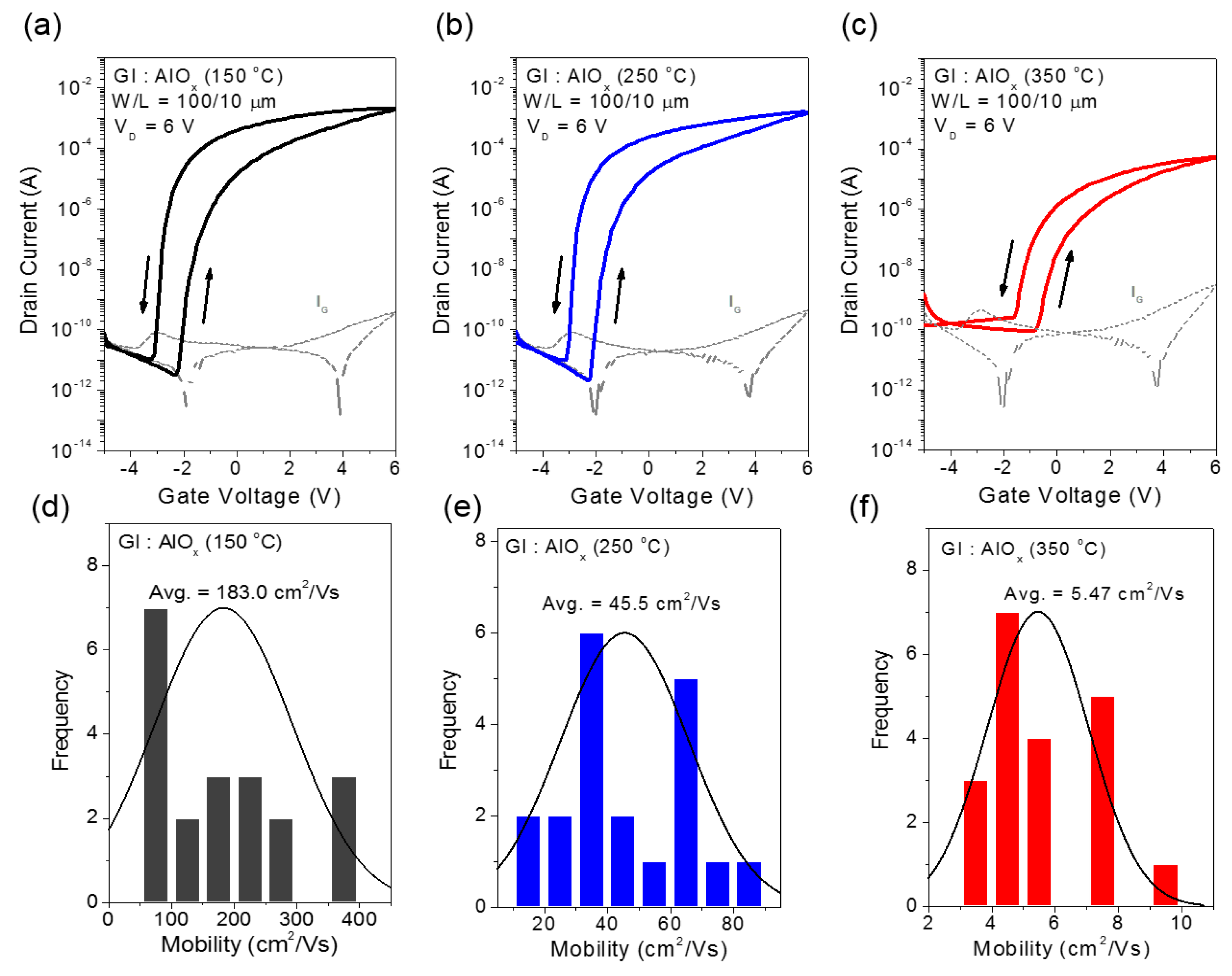
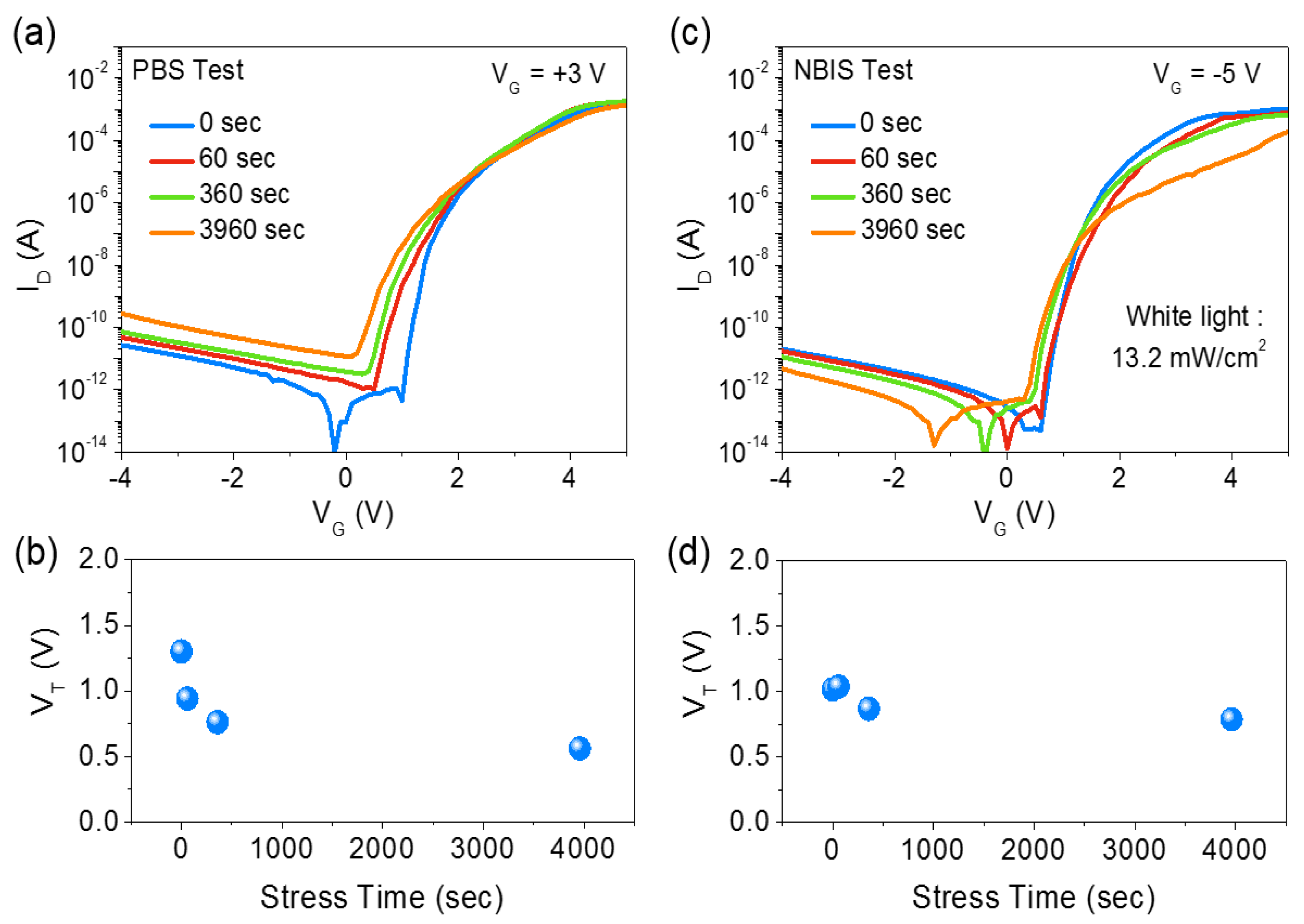
3. Results and Discussion

In order to examine the dielectric properties of solution-processed AlOx and HGD layers, the areal capacitance vs. frequency (C-F) and the current density vs. electric field (J-E) characteristics were measured. In addition, the difference in the surface morphology of AlOx and HGD films is negligible. Figure 2a,b show the areal capacitance vs. frequency data for AlOx and HGD gate dielectrics, respectively. In the case of the AlOx gate dielectric, the capacitance value and the corresponding dielectric constant showed an increasing trend with the annealing temperature. Particularly, with an annealing temperature of 150 °C, the dielectric constant was 7.09 (thickness of 89 nm), but it decreased to 6.11 and 5.11 when the annealing temperature was increased to 350 °C and 450 °C, respectively. In the case of HGD gate dielectric, a similar behavior was observed as shown in Figure 2b. With an annealing temperature of 150 °C, HGD gate dielectric exhibited a dielectric constant of 8.15, and decreased to 6.10 and 6.01 when the annealing temperature was increased to 350 °C and 450 °C, respectively. It should be noted that the areal capacitance value and the corresponding dielectric constant were higher in the HGD gate dielectric, which can be attributed to the mobile ions in the polymer network combined with AlOx film. To further investigate the insulating properties, the current density vs. electric field measurements for AlOx and HGD gate dielectrics were carried out. Figure 2c,d show the current density vs. electric field data for AlOx and HGD gate dielectrics, respectively. In the case of AlOx gate dielectric, even a low temperature annealing of 150 °C resulted in reasonable insulating properties. With the annealing temperature of 150 °C, the leakage current density was 4.45 × 10⁻⁶ A/cm2 at an electric field of 2 MV/cm. Further increasing the annealing temperature to 350 °C and 450 °C improved the insulating properties, and the current density was decreased to 4.44 × 10⁻⁷ A/cm2 and 8.29 × 10⁻¹⁰ A/cm2, respectively. In the case of HGD gate dielectric, even a low temperature annealing of 150 °C resulted in reasonable insulating properties. At an annealing temperature of 150 °C, the leakage current density was 1.47 × 10⁻⁵ A/cm2 at an electric field of 2 MV/cm. Increasing the annealing temperature to 350 °C and 450 °C improved the insulating properties and the current density was decreased to 1.47 × 10⁻⁶ A/cm2 and 2.37 × 10⁻⁹ A/cm2, respectively. Additionally, an AlOx and HGD film with the annealing temperature of 250 °C have insulator properties similar to those of 150 °C-annealed gate dielectric films, while thickness were decreased from 89 to 60 nm. The slightly high leakage current density observed in HGD gate dielectrics provides that a profound number of mobile ions may exist in the gate dielectric layer. However, even with the mobile ions, the leakage current density is reasonably low to be utilized as a gate dielectric layer.
The presence of mobile ions in the solution-processed AlOx and HGD gate dielectrics were further validated by measuring the areal capacitance change as a function of bias polarity. Figure 2e,f show the areal capacitance vs. voltage (C-V) plots for AlOx and HGD gate dielectrics annealed at 150 °C, respectively. Here, the C-V characteristics were obtained using an MIS structure of Si wafer/AlOx(or HGD)/InOx/Al at frequencies of 100 kHz and 1 MHz (inset). As displayed, the areal capacitance increases when the bias polarity changed from negative to positive bias, which can be attributed to the formation of an EDL at the AlOx(or HGD)/InOx interface. Particularly, in the case of AlOx gate dielectric, the hysteresis was comparably larger than that of an HGD gate dielectric, possibly indicating a larger amount of residual mobile ions present in the film. As schematically illustrated in Figure 2g, when a negative bias is applied to the Si wafer, positively charged mobile ions accumulate near the AlOx(or HGD)/Si wafer interface, while the negatively charged mobile ions move toward the AlOx or HGD/InOx interface. Since the majority carrier in the InOx semiconductor is an electron (an n-type), the negatively charged mobile ions near the AlOx(or HGD)/InOx interface repel the electrons in the InOx channel. However, when a positive bias is applied to the Si wafer, the positively charged mobile ions move toward AlOx(or HGD)/InOx interface. Then, these positively charged mobile ions accumulate electrons in the InOx channel, forming an EDL at the AlOx(or HGD)/InOx interface. This in turn increases the areal capacitance of the device. The different capacitance with applied bias frequency may constitute solid evidence of the formation of an EDL layer. The lower capacitance with larger hysteresis at high frequency (1 MHz) is likely due to the less responsive mobile ions inside the AlOx films.
Using the solution-processed AlOx and HGD layers as a gate dielectric, InOx TFTs were fabricated. Figure 3a–c show the transfer characteristics of InOx TFTs fabricated with AlOx gate dielectric layer annealed at different temperatures. In the case of the 150 °C-annealed AlOx gate dielectric, an average field-effect mobility of 183.0 cm2/Vs was observed, which is remarkably high as compared to those made with SiO2 gate dielectrics [23,24]. The exceptionally high mobility observed using the AlOx gate dielectric can be attributed to the formation of an EDL due to a large amount of residual –OHs inside the AlOx films [25]. In addition to the positive gate bias, a substantial number of electrons are accumulated near the AlOx/InOx interface due to the EDL formation. These additional electrons contribute to the drain current resulting in a high drain current and increased field-effect mobility, as well as a large counter-clockwise hysteresis. As mentioned above, the formation of EDL is due to the mobile ions, including –OH residues in the AlOx gate dielectric layer. As shown in Figure 3b,c, the drain current and the field-effect mobility decreased as the annealing temperature increased. Particularly, with annealing temperatures of 250 °C and 350 °C, the field-effect mobility was decreased to 45.5 cm2/Vs and 5.47 cm2/Vs, respectively. At a higher annealing temperature, the number of mobile ions dramatically decreases, which drives the formation of a weak EDL and a low carrier concentration at the AlOx/InOx interface.
In the case of the HGD gate dielectric layer, similar behavior was observed. Figure 4a–c show the transfer characteristics of InOx TFTs fabricated with the HGD gate dielectric layer annealed at different temperatures. The InOx TFTs fabricated with a 150 °C-annealed HGD gate dielectric showed an average field-effect mobility of 120.2 cm2/Vs. Additionally, in the case of 250 °C- and 350 °C-annealed HGD gate dielectrics, field-effect mobilities of 94.3 cm2/Vs and 16.1 cm2/Vs were observed, respectively, showing a similar decreasing trend with the annealing temperature. This decreasing trend of mobility with annealing temperature can also be attributed to the decrease of the mobile ions and corresponding weak EDL formation. The relatively superior mobility in the HGD devices can be described by the aforementioned polymer network confinement of the mobile ions in the HGD [20]. Nonetheless, the solution-processed HGD gate dielectrics allow the acceptable formation of EDL at the gate dielectric/InOx interface, which significantly enhances the electrical properties of InOx TFTs compared to the bare AlOx films. In addition, due to the high dielectric constant and low thickness of the gate dielectric layers, low voltage operation below 6 V was possible, enabling low power consuming electronic devices.
In oxide semiconductor-based TFTs, the operational stabilities under positive gate bias stress (PBS) and negative illumination gate bias stress (NBIS) are important factors. In order to determine the operational stability of InOx TFTs using the HGD gate dielectric, PBS and NBIS tests were carried out. Figure 5a shows the variation of transfer characteristics in InOx TFTs under PBS. Here, the gate bias was set at +3 V, and the transfer curves were measured at 60, 360, and 3960 s. As shown in Figure 5b, the device exhibited reasonably small threshold voltage shift (ΔVT = −1.67 V) during the 3960 s of PBS. Typically, under PBS conditions, oxide TFTs tend to have positive VT shift due to the electron trapping at the gate dielectric/semiconductor interface [26,27,28]. However, in the case of InOx TFTs using the HGD gate dielectric, a negative VT shift was observed. This opposite behavior in VT instability is possibly caused by the mobile ions present in the HGD gate dielectric. Particularly, under a continuous PBS condition, a significant amount of positively charged mobile ions move towards the InOx/HGD interface (Figure 6a). These positive mobile ions, then, contribute to the accumulation of electrons in the InOx channel layer. However, due to the slow responsive characteristic of mobile ions [29,30,31], they tend to remain near the InOx/HGD interface causing a negative shift of transfer curves. In addition, the stability under the NBIS condition was also analyzed. Figure 5c,d show the variation of transfer characteristics and VT under NBIS condition, respectively. Surprisingly, the InOx TFT showed extremely high stability against NBIS and showed ΔVT of −0.23 V (after 3960 s). Typically, the NBIS causes a significant negative VT shift due to the ionization of neutral oxygen vacancies and negative-bias-induced hole injection in the gate dielectric layer [32,33,34,35]. However, the InOx TFT with HGD gate dielectric showed negligible VT shift under a prolonged light illumination and negative bias condition. This significant reduction in the VT shift can be attributed to the neutralization of injected holes with the negatively charged mobile ions near the InOx/HGD interface (Figure 6b). As a consequence, the device can exhibit a high operational stability under NBIS. Furthermore, it should be noted that the InOx TFTs with an HGD dielectric layer exhibited fast recovery after the PBS and NBIS tests. It was found that the VT was recovered to original states after around 6 min, which can be attributed to the gradual neutralization of EDL during the recovery.

4. Conclusions

In this paper, we demonstrated high-mobility, operationally stable InOx TFTs by using ionic-type AlOx and HGD gate dielectrics. The solution-processed AlOx and HGD exhibited reasonably high capacitance and dielectric constant, and only a small decrease in capacitance was observed at high frequencies, enabling a high frequency operation. Using the solution-processed HGD gate dielectrics with 350 °C annealing treatment, solution-processed InOx TFTs were fabricated with an average field-effect mobility of 16.1 cm2/Vs with minimal hysteresis. In addition, the HGD gate dielectric also suppressed the negative VT shift during the NBIS condition, which enhanced the operation stability of the InOx TFTs.

Acknowledgments

This work was partially supported by the Human Resources Development (No. 20154030200860) of the Korea Institute of Energy Technology Evaluation and Planning (KETEP) grant funded by the Korea government Ministry of Trade, Industry and Energy and by the Chung-Ang University Research Scholarship Grants in 2016.

Author Contributions

Jae Sang Heo, Seungbeom Choi, Jeong-Wan Jo, and Jingu Kang performed the experiments and the data analysis. Sung Kyu Park, Yong-Hoon Kim, and Ho-Hyun Park helped draft the manuscript and carry out data analysis and evaluation. Sung Kyu Park and Yong-Hoon Kim made substantial contributions to the concept of experiments and were responsible for leading the project. All authors read and approve the final manuscript.

Conflicts of Interest

The authors declare no conflict of interest.

References

  1. Nomura, K.; Ohta, H.; Ueda, K.; Kamiya, T.; Hirano, M.; Hosono, H. Thin-film transistor fabricated in single-crystalline transparent oxide semiconductor. Science 2003, 300, 1269–1272. [Google Scholar] [CrossRef] [PubMed]
  2. Nomura, K.; Ohta, H.; Takagi, A.; Kamiya, T.; Hirano, M.; Hosono, H. Room-temperature fabrication of transparent flexible thin-film transistors using amorphous oxide semiconductors. Nature 2004, 432, 488–492. [Google Scholar] [CrossRef] [PubMed]
  3. Liu, J.; Buchholz, D.B.; Chang, R.P.H.; Facchetti, A.; Marks, T.J. High-performance flexible transparent thin-film transistors using a hybrid gate dielectric and an amorphous zinc indium tin oxide channel. Adv. Mater. 2010, 22, 2333–2337. [Google Scholar] [CrossRef] [PubMed]
  4. Kim, Y.-H.; Heo, J.-S.; Kim, T.-H.; Park, S.; Yoon, M.-H.; Kim, J.; Oh, M.S.; Yi, G.-R.; Noh, Y.-Y.; Park, S.K. Flexible metal-oxide devices made by room-temperature photochemical activation of sol-gel films. Nature 2012, 489, 128–132. [Google Scholar] [CrossRef] [PubMed]
  5. Lee, S.; Shin, J.; Jang, J. Top Interface Engineering of Flexible Oxide Thin-Film Transistors by Splitting Active Layer. Adv. Funct. Mater. 2017, 27, 1604921. [Google Scholar] [CrossRef]
  6. Rembert, T.; Battaglia, C.; Anders, A.; Javey, A. Room Temperature Oxide Deposition Approach to Fully Transparent, All-Oxide Thin-Film Transistors. Adv. Mater. 2015, 27, 6090–6095. [Google Scholar] [CrossRef] [PubMed]
  7. Banger, K.K.; Yamashita, Y.; Mori, K.; Peterson, R.L.; Leedham, T.; Rickard, J.; Sirringhaus, H. Low-temperature, high-performance solution-processed metal oxide thin-film transistors formed by a “sol–gel on chip” process. Nat. Mater. 2011, 10, 45–50. [Google Scholar] [CrossRef] [PubMed]
  8. Chang, J.; Chang, K.L.; Chi, C.; Zhang, J.; Wu, J. Water induced zinc oxide thin film formation and its transistor performance. J. Mater. Chem. C 2014, 2, 5397. [Google Scholar] [CrossRef]
  9. Pal, B.N.; Dhar, B.M.; See, K.C.; Katz, H.E. Solution-deposited sodium beta-alumina gate dielectrics for low-voltage and transparent field-effect transistors. Nat. Mater. 2009, 8, 898–903. [Google Scholar] [CrossRef] [PubMed]
  10. Jo, J.-W.; Kim, J.; Kim, K.-T.; Kang, J.-G.; Kim, M.-G.; Kim, K.-H.; Ko, H.; Kim, Y.-H.; Park, S.K. Highly Stable and Imperceptible Electronics Utilizing Photoactivated Heterogeneous Sol-Gel Metal-Oxide Dielectrics and Semiconductors. Adv. Mater. 2015, 27, 1182–1188. [Google Scholar] [CrossRef] [PubMed]
  11. Lin, Y.-H.; Faber, H.; Labram, J.G.; Stratakis, E.; Sygellou, L.; Kymakis, E.; Hastas, N.A.; Li, R.; Zhao, K.; Amassian, A.; et al. High Electron Mobility Thin-Film Transistors Based on Solution-Processed Semiconducting Metal Oxide Heterojunctions and Quasi-Superlattices. Adv. Sci. 2015, 2, 1500058. [Google Scholar] [CrossRef] [PubMed]
  12. Ahn, C.H.; Cho, H.K.; Kim, H. Carrier confinement effect-driven channel design and achievement of robust electrical/photostability and high mobility in oxide thin-film transistors. J. Mater. Chem. C 2016, 4, 727–735. [Google Scholar] [CrossRef]
  13. Kim, M.-G.; Kanatzidis, M.G.; Facchetti, A.; Marks, T.J. Low-temperature fabrication of high-performance metal oxide thin-film electronics via combustion processing. Nat. Mater. 2011, 10, 382–388. [Google Scholar] [CrossRef] [PubMed]
  14. Heo, J.S.; Jo, J.W.; Kang, J.; Jeong, C.Y.; Jeong, H.Y.; Kim, S.K.; Kim, K.; Kwon, H.I.; Kim, J.; Kim, Y.H.; et al. Water-Mediated Photochemical Treatments for Low-Temperature Passivation of Metal-Oxide Thin-Film Transistors. ACS Appl. Mater. Interfaces 2016, 8, 10403–10412. [Google Scholar] [CrossRef] [PubMed]
  15. Fujii, M.N.; Ishikawa, Y.; Miwa, K.; Okada, H.; Uraoka, Y.; Ono, S. High-density carrier-accumulated and electrically stable oxide thin-film transistors from ion-gel gate dielectric. Sci. Rep. 2015, 5, 18168. [Google Scholar] [CrossRef] [PubMed]
  16. Cho, J.H.; Lee, J.; He, Y.; Kim, B.; Lodge, T.P.; Frisbie, C.D. High-capacitance ion gel gate dielectrics with faster polarization response times for organic thin film transistors. Adv. Mater. 2008, 20, 686–690. [Google Scholar] [CrossRef]
  17. Tölle, F.J.; Fabritius, M.; Mülhaupt, R. Aerosol Jet Printed p- and n-type Electrolyte-Gated Transistors with a Variety of Electrode Materials Exploring Practical Routes to Printed Electronics. Adv. Funct. Mater. 2012, 22, 1136–1144. [Google Scholar] [CrossRef]
  18. Pudasaini, P.R.; Noh, J.H.; Wong, A.T.; Ovchinnikova, O.S.; Haglund, A.V.; Dai, S.; Ward, T.Z.; Mandrus, D.; Rack, P.D. Ionic Liquid Activation of Amorphous Metal-Oxide Semiconductors for Flexible Transparent Electronic Devices. Adv. Funct. Mater. 2016, 26, 2820–2825. [Google Scholar] [CrossRef]
  19. Pudasaini, P.R.; Noh, J.H.; Wong, A.; Haglund, A.V.; Dai, S.; Ward, T.Z.; Mandrus, D.; Rack, P.D. Ionic Liquid versus SiO2 Gated a-IGZO Thin Film Transistors: A Direct Comparison. ECS J. Solid State Sci. Technol. 2015, 4, Q105–Q109. [Google Scholar] [CrossRef]
  20. Cho, J.H.; Lee, J.; Xia, Y.; Kim, B.; He, Y.; Renn, M.J.; Lodge, T.P.; Daniel Frisbie, C. Printable ion-gel gate dielectrics for low-voltage polymer thin-film transistors on plastic. Nat. Mater. 2008, 7, 900–906. [Google Scholar] [CrossRef] [PubMed]
  21. Ma, H.; Wang, Y.; Wu, D.; Zhang, Y.; Gao, J.; Ren, X.; Du, B.; Wei, Q. A Novel Controlled Release Immunosensor based on Benzimidazole Functionalized SiO2 and Cyclodextrin Functionalized Gold. Sci. Rep. 2016, 6, 19797. [Google Scholar] [CrossRef] [PubMed]
  22. Park, H.; Nam, Y.; Jin, J.; Bae, B.-S. Space charge-induced unusually-high mobility of a solution-processed indium oxide thin film transistor with an ethylene glycol incorporated aluminum oxide gate dielectric. RSC Adv. 2015, 5, 102362–102366. [Google Scholar] [CrossRef]
  23. Kim, M.G.; Kim, H.S.; Ha, Y.G.; He, J.; Kanatzidis, M.G.; Facchetti, A.; Marks, T.J. High-performance solution-processed amorphous zinc-indium-tin oxide thin-film transistors. J. Am. Chem. Soc. 2010, 132, 10352–10364. [Google Scholar] [CrossRef] [PubMed]
  24. Rim, Y.S.; Chen, H.; Kou, X.; Duan, H.S.; Zhou, H.; Cai, M.; Kim, H.J.; Yang, Y. Boost up mobility of solution-processed metal oxide thin-film transistors via confining structure on electron pathways. Adv. Mater. 2014, 26, 4273–4278. [Google Scholar] [CrossRef] [PubMed]
  25. Banger, K.; Warwick, C.; Lang, J.; Broch, K.; Halpert, J.E.; Socratous, J.; Brown, A.; Leedham, T.; Sirringhaus, H. Identification of dipole disorder in low temperature solution processed oxides: Its utility and suppression for transparent high performance solution-processed hybrid electronics. Chem. Sci. 2016, 10, 45–50. [Google Scholar] [CrossRef] [PubMed]
  26. Kimura, M.; Nakanishi, T.; Nomura, K.; Kamiya, T.; Hosono, H. Trap densities in amorphous-InGaZnO4 thin-film transistors. Appl. Phys. Lett. 2008, 92, 13–16. [Google Scholar] [CrossRef]
  27. Seo, J.-S.; Bae, B.-S. Improved Electrical Performance and Bias Stability of Solution-Processed Active Bilayer Structure of Indium Zinc Oxide based TFT. ACS Appl. Mater. Interfaces 2014, 6, 15335–15343. [Google Scholar] [CrossRef] [PubMed]
  28. Chen, W.T.; Lo, S.Y.; Kao, S.C.; Zan, H.W.; Tsai, C.C.; Lin, J.H.; Fang, C.H.; Lee, C.C. Oxygen-dependent instability and annealing/passivation effects in amorphous In-Ga-Zn-O thin-film transistors. IEEE Electron Device Lett. 2011, 32, 1552–1554. [Google Scholar] [CrossRef]
  29. Narasimhan, V.; Park, S.Y. An Ion Gel as a Low-Cost, Spin-Coatable, High-Capacitance Dielectric for Electrowetting-on-Dielectric (EWOD). Langmuir 2015, 31, 8512–8518. [Google Scholar] [CrossRef] [PubMed]
  30. Larsson, O.; Said, E.; Berggren, M.; Crispin, X. Insulator polarization mechanisms in polyelectrolyte-gated organic field-effect transistors. Adv. Funct. Mater. 2009, 19, 3334–3341. [Google Scholar] [CrossRef]
  31. Nketia-Yawson, B.; Kang, S.-J.; Tabi, G.D.; Perinot, A.; Caironi, M.; Facchetti, A.; Noh, Y.-Y. Ultrahigh Mobility in Solution-Processed Solid-State Electrolyte-Gated Transistors. Adv. Mater. 2017, 29, 1605685. [Google Scholar] [CrossRef] [PubMed]
  32. Chowdhury, M.D.H.; Migliorato, P.; Jang, J. Light induced instabilities in amorphous indium-gallium-zinc-oxide thin-film transistors. Appl. Phys. Lett. 2010, 97, 10–13. [Google Scholar] [CrossRef]
  33. Rim, Y.S.; Jeong, W.; Ahn, B.D.; Kim, H.J. Defect reduction in photon-accelerated negative bias instability of InGaZnO thin-film transistors by high-pressure water vapor annealing. Appl. Phys. Lett. 2013, 102, 143503. [Google Scholar]
  34. Jo, J.-W.; Kim, Y.-H.; Park, S.K. Light-induced hysteresis and recovery behaviors in photochemically activated solution-processed metal-oxide thin-film transistors. Appl. Phys. Lett. 2014, 105, 43503. [Google Scholar] [CrossRef]
  35. Ueoka, Y.; Ishikawa, Y.; Bermundo, J.P.; Yamazaki, H.; Urakawa, S.; Fujii, M.; Horita, M.; Uraoka, Y. Density of States in Amorphous In-Ga-Zn-O Thin-Film Transistor under Negative Bias Illumination Stress. ECS J. Solid State Sci. Technol. 2014, 3, Q3001–Q3004. [Google Scholar] [CrossRef]
Figure 1. (a) Schematic illustration of InOx TFTs using AlOx or HGD gate dielectric layer; (b) Photographs of an HGD solution before and after a thermal cross-linking.
Materials 10 00612 g001
Figure 2. Electrical characteristics for solution-processed AlOx or HGD dielectric layer using metal-insulator-metal structure (MIM; Si/AlOx or HGD/Al) with the different annealing conditions (at 150, 250, 350, and 450 °C). The areal capacitance per area-frequency (C-F) of solution-processed (a) AlOx and (b) HGD dielectric layer; leakage current density-electric field (J-E) of solution-processed (c) AlOx and (d) HGD dielectric layer; the C-V characteristics of an (e) AlOx and (f) HGD gate dielectric (150 °C) at 100 kHz and 1 MHz (inset) using metal-insulator-semiconductor structure (MIS; Si/AlOx or HGD/InOx/Al); (g) the polarization mechanisms and electric double layer formation in InOx TFTs with HGD dielectric layer.
Materials 10 00612 g002
Figure 3. Electrical characteristics of various solution-processed InOx TFTs on an AlOx dielectric layer for the different processed conditions. The transfer curves for InOx TFTs with (a) 150 °C-annealed; (b) 250 °C-annealed; and (c) 350 °C-annealed AlOx films; the dotted lines indicate the gate leakage current. Statistical distribution of field-effect mobilities for InOx TFTs with (d) 150 °C-annealed; (e) 250 °C-annealed; and (f) 350 °C-annealed AlOx films.
Materials 10 00612 g003
Figure 4. Electrical characteristics of various solution-processed InOx TFTs on an HGD dielectric layer for the different processed conditions. The transfer curves for InOx TFTs with (a) 150 °C-annealed; (b) 250 °C-annealed; and (c) 350 °C-annealed HGD films. The dotted lines indicate the gate leakage current. Statistical distribution of field-effect mobilities for InOx TFTs with (d) 150 °C-annealed; (e) 250 °C-annealed; and (f) 350 °C-annealed HGD films.
Materials 10 00612 g004
Figure 5. (a) Positive gate bias stability and (b) evolution of threshold voltage (VT) of solution-processed InOx TFTs with the 150 °C-annealed HGD dielectric layer (VGS = +3 V, t = 3960 s); (c) negative gate bias illumination stability and (d) evolution of threshold voltage (VT) of solution-processed InOx TFTs with the 150 °C-annealed HGD dielectric layer (VGS = −5 V, t = 3960 s).
Materials 10 00612 g005
Figure 6. Schematic and energy band diagrams of corresponding VT instability of solution-processed InOx TFT with the 150 °C-annealed HGD dielectric layer for (a) PBS and (b) NBIS tests.
Materials 10 00612 g006

