Ultra Thin Poly-Si Nanosheet Junctionless Field-Effect Transistor with Nickel Silicide Contact

1
Department of Engineering and System Science, National Tsing Hua University, Hsinchu 30013, Taiwan
2
Department of Electrical Engineering, National United University, Miao-Li 36063, Taiwan
*
Author to whom correspondence should be addressed.
Materials 2017, 10(11), 1276; https://doi.org/10.3390/ma10111276
Submission received: 21 September 2017
/
Revised: 18 October 2017
/
Accepted: 2 November 2017
/
Published: 7 November 2017
(This article belongs to the Section Advanced Materials Characterization)
Abstract
:This study demonstrated an ultra thin poly-Si junctionless nanosheet field-effect transistor (JL NS-FET) with nickel silicide contact. For the nickel silicide film, two-step annealing and a Ti capping layer were adopted to form an ultra thin uniform nickel silicide film with low sheet resistance (Rs). The JL NS-FET with nickel silicide contact exhibited favorable electrical properties, including a high driving current (>107A), subthreshold slope (186 mV/dec.), and low parasitic resistance. In addition, this study compared the electrical characteristics of JL NS-FETs with and without nickel silicide contact.
1. Introduction
Metal silicide techniques have been developed at the deep submicron level in microelectronics as contact materials to the source, drain, and gate regions [1,2,3]. Nickel silicides are valuable electronic materials used as contacts for field-effect transistors, as interconnects, and in nanoelectronic devices because of their source/drain (S/D) sheet resistance. To replace the currently used cobalt silicide and titanium silicide, nickel silicide has attracted attention as a candidate for future nodes because of advantages including low temperature processing, low silicon consumption, no bridging failure property, low mechanical stress, and low contact resistance [4,5,6]. Notably, the diffusion-controlled reaction of Ni silicidation formation occurs by Ni diffusion into the silicon area. The Ni vacancies generated by themselves are mainly located in the Ni layer instead of in the Si layer [3,7]. As device dimensions are scaled down, lowering sheet resistance is a critical factor in applications where silicides are used. Nickel silicide has some limitations, such as (1) interfacial silicon oxide present at the Ni/Si interface hampering the silicidation between Ni and Si, (2) the thermal stability of nickel silicide, and (3) the need to reduce the junction leakage current of nickel-silicided junctions [8,9].
A Ti capping layer can prevent oxygen adsorption on deposited nickel silicide [10,11,12], and can also prevent oxidation during the silicidation process because it is an excellent oxygen scavenger. Other advantages of Ti capping include increased uniformity and thermal stability, as well as a low junction leakage current. Furthermore, the development of metal silicide technology through two-step rapid thermal annealing (RTA) has been extensively investigated as a low resistance contact [13,14]. The first step involves low temperature annealing to drive nickel to diffuse into Si, to thus form a nickel-rich silicide layer. The second step involves higher temperature annealing to transform the nickel silicide phase.
A junctionless field-effect transistor (JL-FET) can be fabricated simply by heavily doping the channel and S/D regions simultaneously. Because of the special doping profile, JL-FETs have several advantages such as a low thermal budget that can integrate with high-k/metal-gate more easily than can conventional metal–oxide–semiconductor field-effect transistors (MOSFETs), a longer effective channel length than conventional MOSFETs, and the avoidance of complicated S/D engineering. To solve the JL-FET turn-off problem, an ultrathin body structure is required to achieve a fully-depleted channel region in the off state [15,16,17]. However, the drive current (ID) declines as transistor features are scaled. Therefore, the study presents an ultra thin poly-Si junctionless nanosheet field-effect transistor (JL NS-FET) with a nickel silicide contact. Moreover, this study presents results obtained from nickel silicide that indicate the state of the substrate and the silicide phase. Nickel silicide quality was analyzed using X-ray diffraction (XRD), transmission-electron microscopy (TEM), and a four-point probe (FPP).
2. Silicide Film Analysis
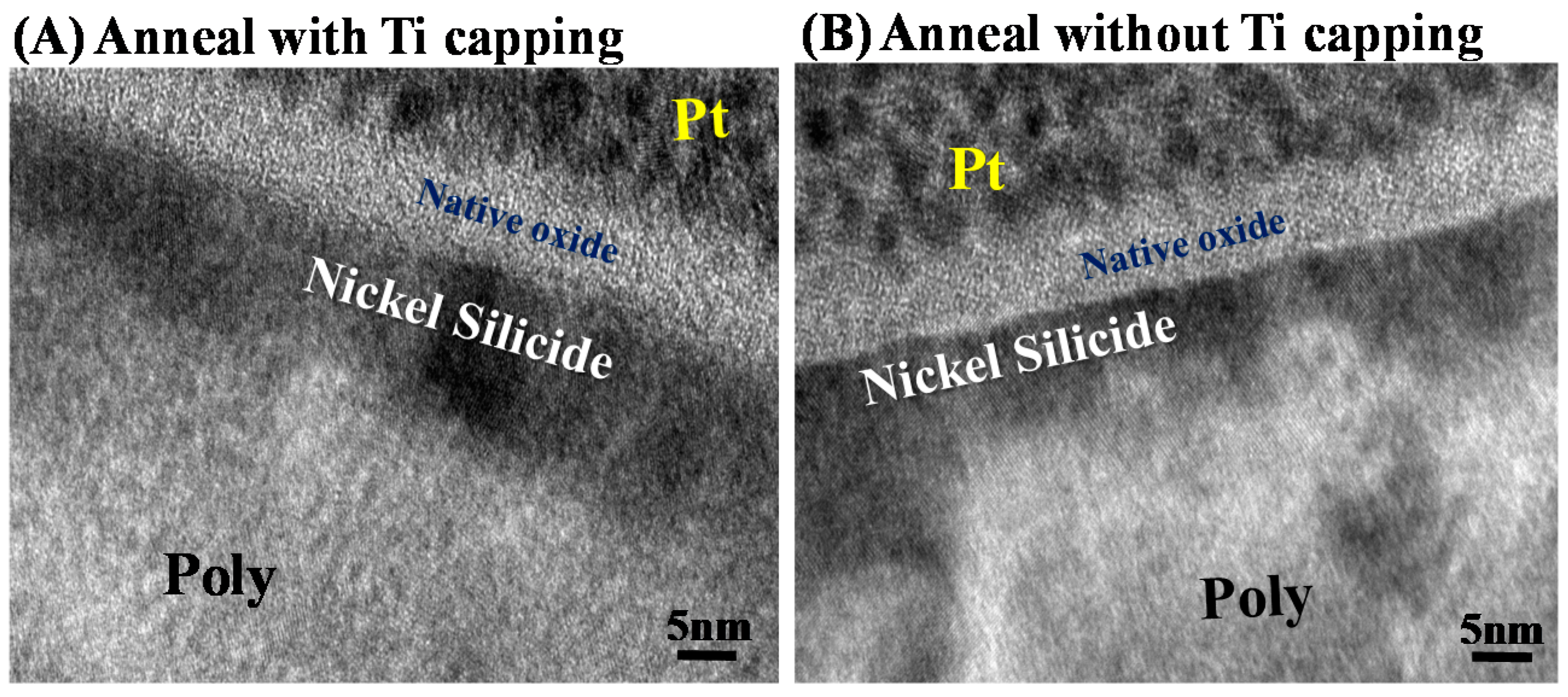
Figure 1 displays the key process flow diagram and schematics of nickel silicide film fabrication. The nickel silicide film was fabricated by initially depositing a 50-nm-thick layer of undoped amorphous Si (a-Si) through low pressure chemical vapor deposition (LPCVD) at 550 °C. A poly-Si layer was then formed through solid-phase recrystallization (SPC) at 600 °C for 24 h [18]. Subsequently, a 15-nm-thick nickel film and 10-nm-thick titanium film were deposited through physical chemical deposition (PVD). The films were first annealed through rapid thermal annealing at 260 °C for 30 s to form a nickel silicide film. The unreacted nickel and titanium films were removed by selective etching with sulfuricacid solution at 120 °C. In the second step, rapid thermal annealing was performed at 450 °C for 30 s to lower the sheet resistance and firmly merge the phase (Figure 4). Figure 2 displays high-resolution TEM images for the first annealing process with and without titanium capping. As shown in Figure 2A, the nickel silicide film formed through the first annealing with Ti capping was uniform because the Ti capping layer suppressed the oxidation of the nickel silicide films. This serves as evidence that a Ti capping layer is an oxygen scavenger. Oxygen is a pollutant in the silicide process and reduces the quality of nickel silicide film, as indicated in Figure 2B.
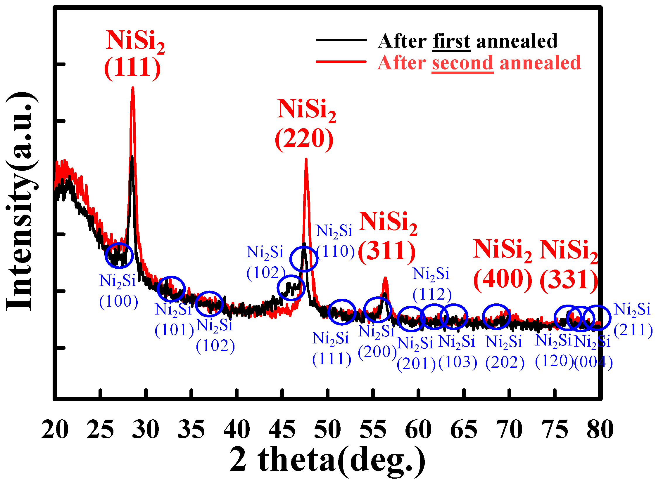
Figure 3 displays TEM images of the nickel silicide film after the first and second annealing processes. The second annealing, which exhibited a superior crystal phase than the first annealing, was utilized to lower the sheet resistance and steadily merge the phase (Figure 4). The FPP revealed that the sheet resistance of nickel silicide film was 462.8 ± 20 Ω/sq after the first annealing and 108.7 ± 1 Ω/sq after the second annealing. Figure 4 shows the phase of the nickel silicide film captured by XRD, revealing that the degradation at the second annealing was a result of the phase transformation of Ni2Si to NiSi2 and agglomeration. Thus, after the second annealing, nickel was redistributed in the silicide instead of the underlying silicon being penetrated.
Figure 3.
TEM images for nickel silicide film after (A) the first and (B) the second annealing processes.
Figure 3.
TEM images for nickel silicide film after (A) the first and (B) the second annealing processes.
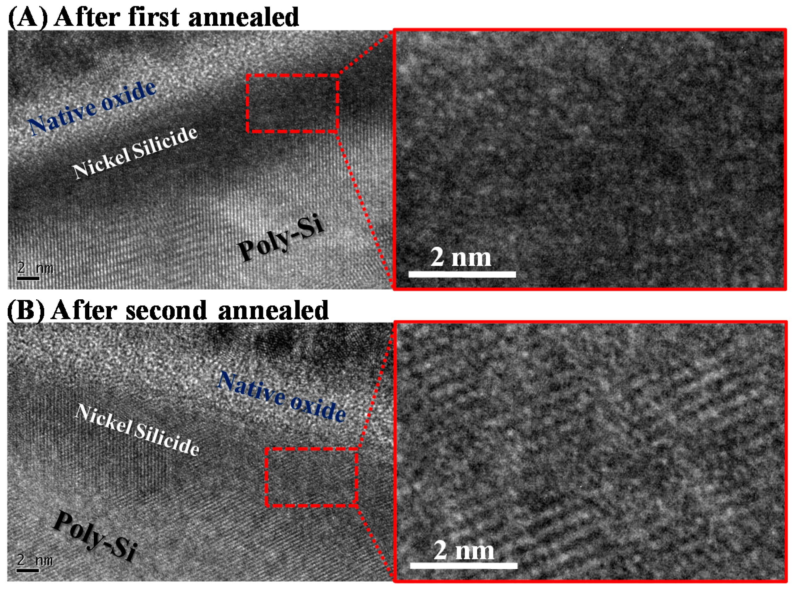
Figure 4.
XRD phase analysis for the nickel silicide film after the first and second annealing processes.
Figure 4.
XRD phase analysis for the nickel silicide film after the first and second annealing processes.

3. Device Structure and Fabrication
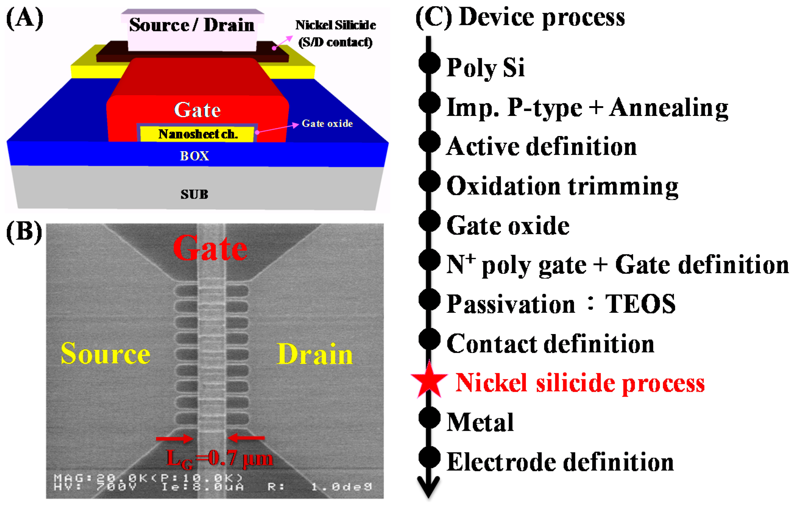
Figure 5A presents a schematic of a single nanosheet cross-section of an ultra thin poly-Si JL NS-FET with a nickel silicide contact. A conventional JL NS-FET without nickel silicide contact was also fabricated for comparison. Figure 5B shows a top-view scanning electron microscope (SEM) image of the 10-strip nanosheets active region with a gate length of 0.7 µm. The gate covers 10 nanosheet strips with a printed width of 100 nm, which formed a sheet-shaped structure. Figure 5C displays the process flow for fabricating the JL NS-FET. The device was fabricated by initially growing a 400-nm-thick thermal SiO2 layer on a 6-inch Si wafer. In addition, a 50-nm-thick layer of undoped a-Si was deposited through LPCVD at 550 °C. The poly-Si layer was then formed using the SPC method at 600 °C for 24 h. The p-channel of the poly-Si layer was implanted with BF2 ions at a dose of 2 × 1014 cm−2 by 30 keV. The dopant was then activated through furnace annealing at 600 °C for 4 h in nitrogen ambient. The nanosheet channels were patterned using e-beam lithography (EBL) and transferred using reactive-ion etching (RIE).
To form the ultra thin poly-Si nanosheet channel, the naked nanosheets were first thermally oxidized and the oxide layer was subsequently removed through hydrogen fluoride dipping. After active region patterning, an 8-nm-thick thermal oxide layer was deposited as the gate oxide layer. A 150-nm-thick in-situ n+ poly-Si deposition was performed as a gate electrode and patterned using EBL and RIE. Subsequently, a 250-nm-thick passivation layer of tetraethoxysilane (TEOS) was deposited. After contact region patterning through EBL and RIE, a 15-nm nickel film and 10-nm titanium film were deposited using PVD. The device was then annealed through rapid thermal annealing (RTA) at 260 °C for 30 s and the unreacted nickel film and titanium film were selectively etched using wet etching for 10 min at 120 °C. RTA was performed a second time at 450 °C for 30 s to lower the sheet resistance and firmly merge the phase. Finally, 300-nm-thick Al–Si–Cu metallization was performed and sintered at 400 °C for 30 min.
4. Results and Discussion
Figure 6A displays across-sectional focused ion beam (FIB) image of the JL NS-FET along the gate direction (A–A’), revealing the 10-strip nanosheet structure. Figure 6B displays TEM images of the nanosheet channel perpendicular to the gate direction of the JL NS-FET. The poly-Si nanosheet assumed the form of a sheet and was surrounded by the N+ poly-Si gate to form a tri-gate structure. The magnified image of the single nanosheet reveals that the width and height were 85.6 and 4.6 nm, respectively. The effective width (Weff) for the JL NS-FET was 85.6 × 10 nm. The gate oxide thickness of the JL NS-FET was approximately 8.8 nm.
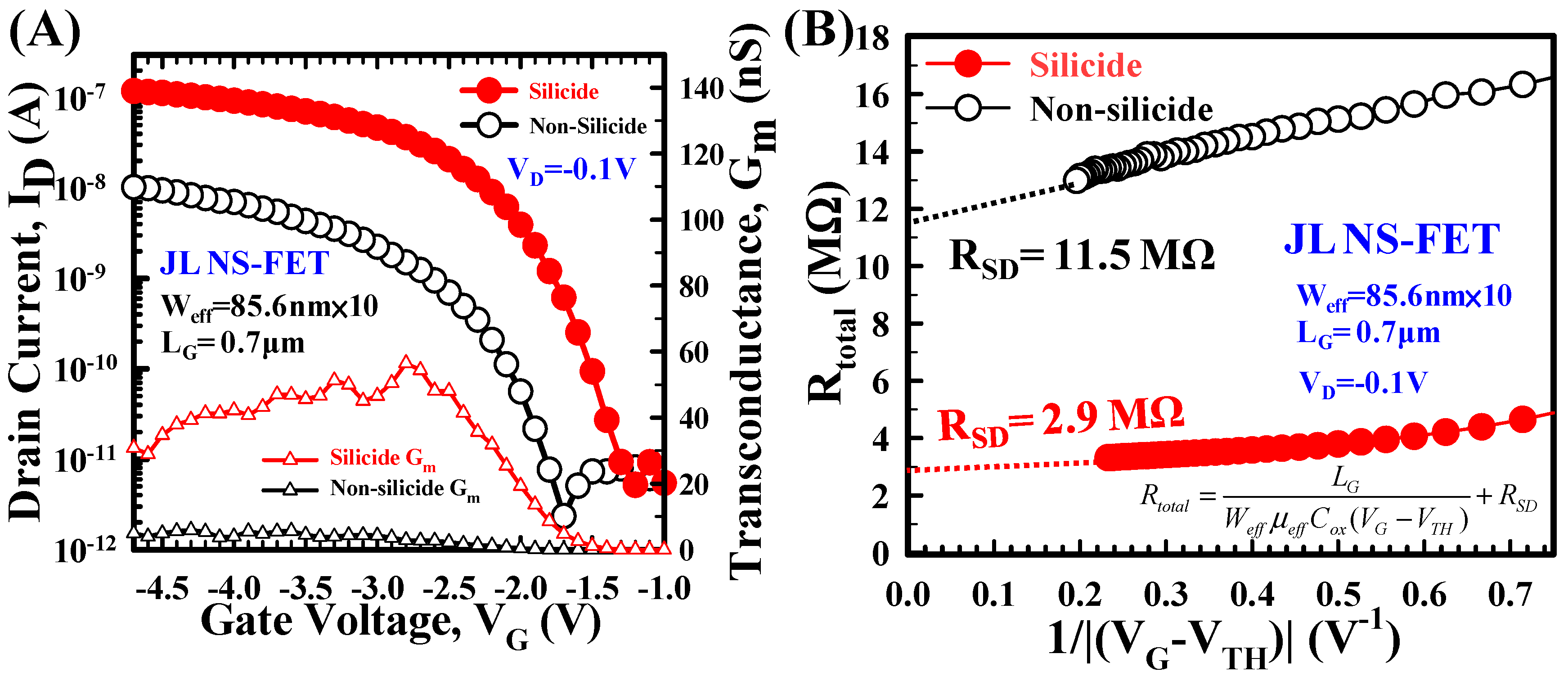
Figure 7A exhibits the ID–VG curves of the JL NS-FET with a nickel silicide contact (silicide) and without (nonsilicide). The subthreshold slopes of the silicide and nonsilicide JL NS-FET were 186 mV/dec. and 194 mV/dec., and the corresponding threshold voltages (VTH) were −1.8 V and −2.3 V, where VTH refers to the gate voltage at ID = 10−9. The silicide JL NS-FET had a superior Ion/Ioff current ratio (2.9 × 10⁴) than did the nonsilicide device. The linear scale of the ID–VG curves shows that the silicide JL NS-FET had six times the saturation current of its nonsilicide counterpart (the inset in Figure 7A displays the linear scale). Figure 7B plots the ID–VD characteristics of the silicide and nonsilicide JL NS-FETs. The saturation current of the silicide device was approximately 3.25 times that of the nonsilicide device at VG − VTH = −3 V and VD = −3 V. The silicide device had a higher saturation current because of its lower S/D parasitic resistance, as shown in Figure 8B.
Figure 8A demonstrates the transfer ID–VG characteristics and transconductance (Gm) of the silicide and nonsilicide JL NS-FETs at VD = −0.1 V. The maximum Gm values were 56.5 and 9 nS at VG = −2.8 V for the silicide and nonsilicide devices, respectively. The field-effect mobilities of the silicide and nonsilicide devices calculated from the maximum Gm at VD = −0.1 V were 8.4 and 1.3 cm2/Vs, respectively. Figure 8B displays the total resistance (Rtotal) curves calculated based on the ID–VG characteristics. The RSD of the silicide and nonsilicide contact devices were 2.9 and 11.5 MΩ where the X-axis was equal to 0, respectively.
5. Conclusions
An ultra thin poly-Si JL NS-FET with nickel silicide contact was demonstrated successfully, exhibiting a high driving current (>107 Å), subthreshold slope (186 mV/dec.), and low parasitic resistance. In the silicide film analysis, the second annealing step was applied to lower the sheet resistance and firmly merged the phase of the silicide film. Additionally, we used a Ti capping layer to remove interfacial oxides on the Si surface and promote a silicidation reaction between Ni and Si. In summary, the JL NS-FET with nickel silicide contact exhibited competitive short-channel behavior and improved drive current.
Acknowledgments
The authors acknowledge the National Science Council of Taiwan for supporting this research under contract number MOST-105-2221-E-239-032 and the National Nano Device Laboratories (NDL) for their technical support.
Author Contributions
Y.-H.L. and Y.-C.W. conceived and designed the experiments. Y.-R.L. and W.-T.T. performed the experiments and analyzed the data. Y.-C.W. contributed reagents, materials, and analysis tools. Y.-R.L. and Y.-H.L. composed the manuscript.
Conflicts of Interest
The authors declare no conflict of interest. The founding sponsors had no role in the design of the study; in the collection, analyses, or interpretation of data; in the writing of the manuscript, and in the decision to publish the results.
References
- Olowolafe, J.O.; Nicolet, M.A.; Mayer, J.W. Influence of the Nature of the Si Substrate on Nickel Silicide Formed from Thin Ni Films. Thin Solid Films 1976, 38, 143–150. [Google Scholar] [CrossRef]
- Morimoto, T.; Momose, H.S.; Iinuma, T.; Kunishima, I.; Suguro, K.; Okana, H.; Katakabe, I.; Nakajima, H.; Tsuchiaki, M.; Ono, M.; et al. A Nisi Salicide Technology for Advanced Logic Devices. In Proceedings of the International Electron Devices Meeting 1991 [Technical Digest], Washington, DC, USA, 8–11 December 1991; pp. 653–656. [Google Scholar]
- Iwai, H.; Ohguro, T.; Ohmi, S.-I. NiSiSalicide Technology for Scaled CMOS. Microelectron. Eng. 2002, 60, 157–169. [Google Scholar] [CrossRef]
- Kittl, J.A.; Lauwers, A.; Chamirian, O.; Van Dal, M.; Akheyar, A.; De Potter, M.; Lindsay, R.; Maex, K. Ni- and Co-Based Silicides for Advanced CMOS Applications. Microelectron. Eng. 2003, 70, 158–165. [Google Scholar] [CrossRef]
- Vengurlekar, A.; Balasubramanian, S.; Ashok, S.; Theodore, D.; Chi, D.Z. Effect of Silicon Substrate Hydrogenation Treatment on Nickel Silicide Formation. In Proceedings of the Fourth International Workshop on Junction Technology, Shanghai, China, 15–16 March 2004; pp. 123–126. [Google Scholar]
- Dahal, A.; Gunasekera, J.; Harringer, L.; Singh, D.K.; Singh, D.J. Metallic Nickel Silicides: Experiments and Theory for NiSi and First Principles Calculations for Other Phases. J. Alloy Compd. 2016, 672, 110–116. [Google Scholar] [CrossRef]
- Lavoie, C.; d’Heurle, F.M.; Detavernier, C.; Cabral, C. Towards Implementation of a Nickel Silicide process for CMOS Technologies. Microelectron. Eng. 2003, 70, 144–157. [Google Scholar] [CrossRef]
- Huang, W.; Zhang, L.-C.; Gao, Y.-Z.; Jin, H.-Y.; Ning, B.-J.; Zhang, G.-Q. Effect of a Thin w Interlayer on the Thermal Stability and Electrical Characteristics of NiSi Film. J. Vac. Sci. Technol. B Microelectron. Nanom. Struct. Proc. Meas. Phenom. 2005, 23, 2304–2308. [Google Scholar] [CrossRef]
- Vengurlekar, A.; Balasubramanian, S.; Ashok, S.; Theodore, D.; Chi, D. Influence of Hydrogen Plasma Surface Treatment of Si Substrate on Nickel Silicide Formation. J. Vac. Sci. Technol. B Microelectron. Nanom. Struct. Proc. Meas. Phenom. 2006, 24, 1449–1454. [Google Scholar] [CrossRef]
- Tan, W.L.; Pey, K.L.; Chooi, S.Y.M.; Ye, J.H.; Osipowicz, T. Effect of a Titanium Cap in Reducing Interfacial Oxides in the Formation of Nickel Silicide. J. Appl. Phys. 2002, 91, 2901–2909. [Google Scholar] [CrossRef]
- Toledo, N.G.; Lee, P.S.; Pey, K.L. Characterization of the Junction Leakage of Ti-Capped Ni-Silicided Junctions. Thin Solid Films 2004, 462, 202–208. [Google Scholar] [CrossRef]
- Guo-Ping, R.; Yu-Long, J.; Xin-Ping, Q.; Bing-Zong, L. Ti-Capping and Heating Ramp-Rate Effects on Ni-Silicide Film and Interface. In Proceedings of the Extended Abstracts of the Fifth International Workshop on Junction Technology, Osaka, Japan, 7–8 June 2005; pp. 83–88. [Google Scholar]
- Ho, C.-Y.; Chang, Y.-J. Evaluation of Schottky Barrier Source/Drain Contact on Gate-all-around Polycrystalline Silicon Nanowire Mosfet. Mater. Sci. Semicond. Proc. 2017, 61, 150–155. [Google Scholar] [CrossRef]
- Zhenping, W.; Xinhua, C.; Jingxun, F. Nickel Silicide Anneal Process Research for 28nm CMOS Node. In Proceedings of the 2017 China Semiconductor Technology International Conference (CSTIC), Shanghai, China, 12–13 March 2017; pp. 1–4. [Google Scholar]
- Yeh, M.S.; Wu, Y.C.; Wu, M.H.; Jhan, Y.R.; Chung, M.H.; Hung, M.F. High Performance Ultra-Thin Body (2.4 nm) Poly-Si Junctionless Thin Film Transistors with a Trench Structure. In Proceedings of the 2014 IEEE International Electron Devices Meeting, San Francisco, CA, USA, 15–17 December 2014. [Google Scholar]
- Yeh, M.S.; Wu, Y.C.; Wu, M.H.; Chung, M.H.; Jhan, Y.R.; Hung, M.F. Characterizing the Electrical Properties of a Novel Junctionless Poly-Si Ultrathin-Body Field-Effect Transistor Using a Trench Structure. IEEE Electron. Device Lett. 2015, 36, 150–152. [Google Scholar] [CrossRef]
- Thirunavukkarasu, V.; Jhan, Y.-R.; Liu, Y.-B.; Kurniawan, E.D.; Lin, Y.R.; Yang, S.-Y.; Cheng, C.-H.; Wu, Y.-C. Gate-all-around Junctionless Silicon Transistors with Atomically Thin Nanosheet Channel (0.65 nm) and Record Sub-Threshold Slope (43 mv/dec). Appl. Phys. Lett. 2017, 110, 032101. [Google Scholar] [CrossRef]
- Tüzün Özmen, Ö.; Karaman, M.; Turan, R. Polysilicon Thin Films Fabricated by Solid Phase Crystallization Using Reformed Crystallization Annealing Technique. Thin Solid Films 2014, 551, 181–187. [Google Scholar] [CrossRef]
Figure 1.
Key process flow diagram and schematics of nickel silicide film.
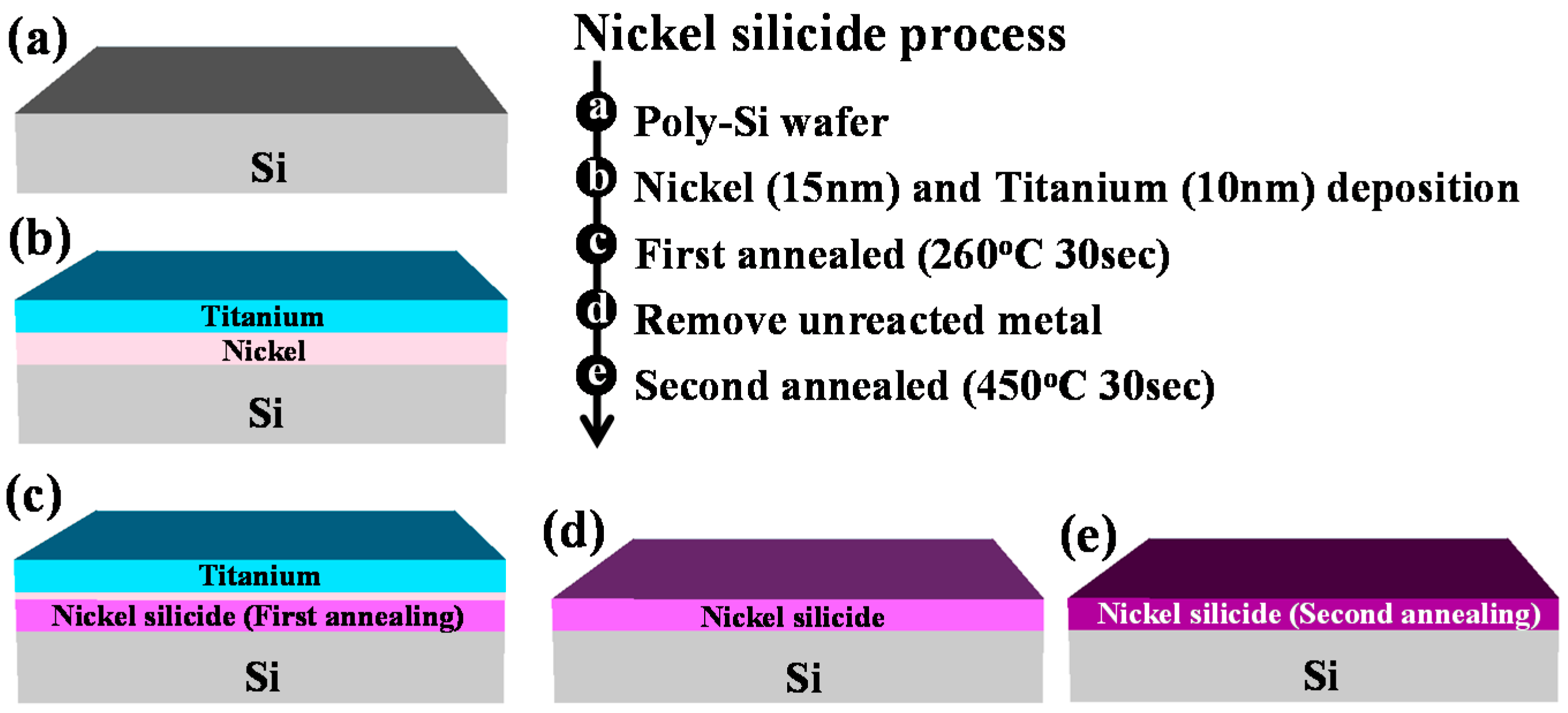
Figure 2.
TEM images for annealing process (A) with and (B) without titanium capping on nickel.

Figure 5.
(A) Schematics of a single nanosheet cross-section; (B) Top-view SEM image of the junctionless nanosheet field-effect transistor (JL NS-FET) structure with 10 nanosheets; (C) Process flow of the JL NS-FET.
Figure 5.
(A) Schematics of a single nanosheet cross-section; (B) Top-view SEM image of the junctionless nanosheet field-effect transistor (JL NS-FET) structure with 10 nanosheets; (C) Process flow of the JL NS-FET.

Figure 6.
(A) Focused ion beam (FIB) section of the SEM image of a cross-sectional view of the JL NS-FET; (B)TEM image of the single nanosheet cross-sectional structure and magnified image.
Figure 6.
(A) Focused ion beam (FIB) section of the SEM image of a cross-sectional view of the JL NS-FET; (B)TEM image of the single nanosheet cross-sectional structure and magnified image.
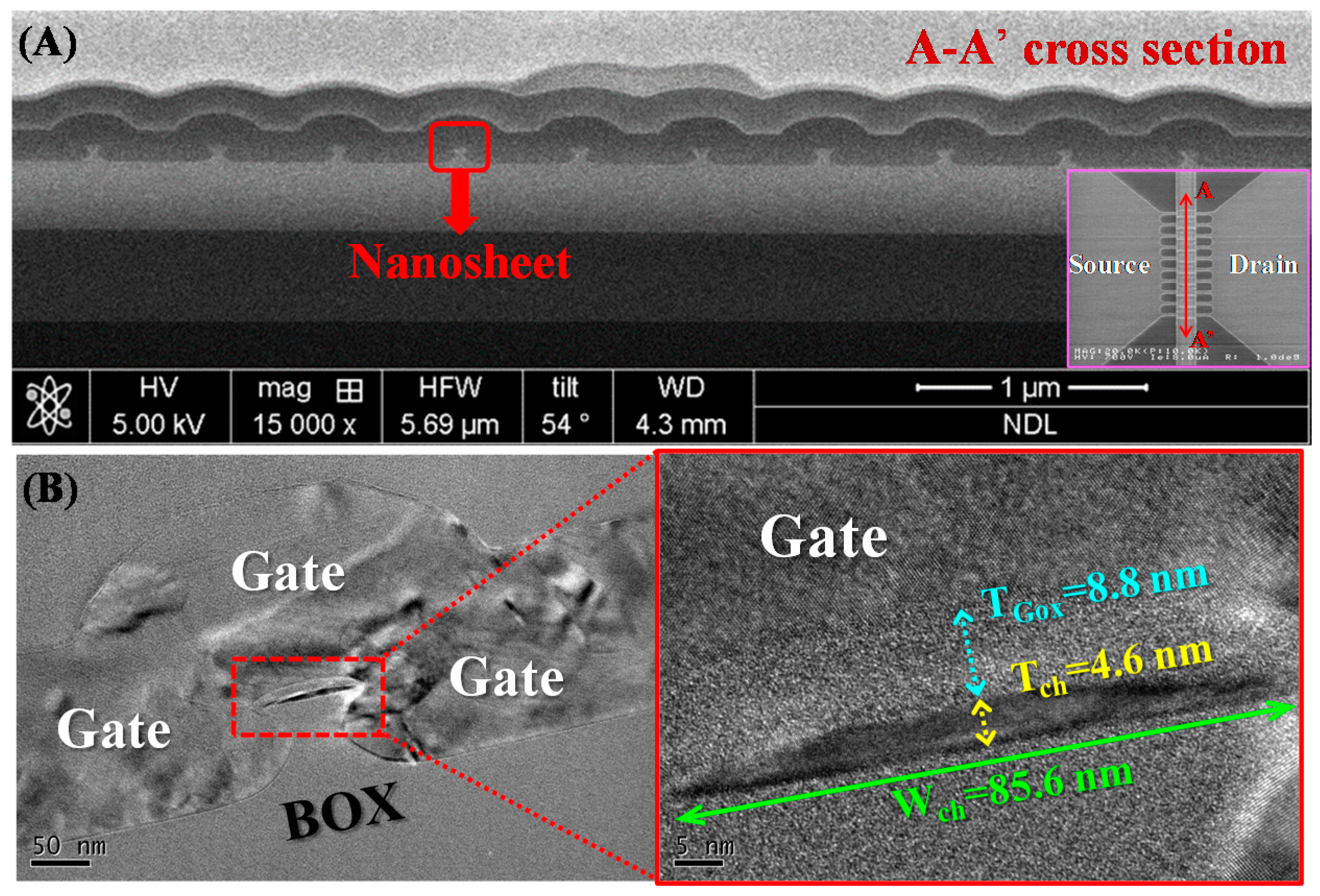
Figure 7.
(A) ID–VG curves of the silicide and nonsilicide JL NS-FETs. The linear scale of the ID–VG curves indicates that the silicide JL NS-FET had 6 times the saturation current of the nonsilicide device(the inset displays the linear scale); (B) Transfer ID–VD curves of the silicide and nonsilicide JL NS-FETs for various VG−VTH values.

Figure 8.
(A) ID–VG curves and Gm of the silicide and nonsilicide JL NS-FETs. The Gm value of the silicide device is larger than that of the nonsilicide device; (B)Total resistance (Rtotal) of the silicide and nonsilicide devices as a function of gate voltage at VD = 0.1 V.
Figure 8.
(A) ID–VG curves and Gm of the silicide and nonsilicide JL NS-FETs. The Gm value of the silicide device is larger than that of the nonsilicide device; (B)Total resistance (Rtotal) of the silicide and nonsilicide devices as a function of gate voltage at VD = 0.1 V.
© 2017 by the authors. Licensee MDPI, Basel, Switzerland. This article is an open access article distributed under the terms and conditions of the Creative Commons Attribution (CC BY) license (http://creativecommons.org/licenses/by/4.0/).
Share and Cite
MDPI and ACS Style
Lin, Y.-R.; Tsai, W.-T.; Wu, Y.-C.; Lin, Y.-H. Ultra Thin Poly-Si Nanosheet Junctionless Field-Effect Transistor with Nickel Silicide Contact. Materials 2017, 10, 1276. https://doi.org/10.3390/ma10111276
AMA Style
Lin Y-R, Tsai W-T, Wu Y-C, Lin Y-H. Ultra Thin Poly-Si Nanosheet Junctionless Field-Effect Transistor with Nickel Silicide Contact. Materials. 2017; 10(11):1276. https://doi.org/10.3390/ma10111276
Chicago/Turabian StyleLin, Yu-Ru, Wan-Ting Tsai, Yung-Chun Wu, and Yu-Hsien Lin. 2017. "Ultra Thin Poly-Si Nanosheet Junctionless Field-Effect Transistor with Nickel Silicide Contact" Materials 10, no. 11: 1276. https://doi.org/10.3390/ma10111276
Note that from the first issue of 2016, this journal uses article numbers instead of page numbers. See further details here.