1. Introduction
Electric Power Research Institute (EPRI) reviewed the feasibility of an intelligent semiconductor transformer that can replace the existing transformer consisting of iron core and coil. Based on this review, a prototype of 4.16 kV 20 kVA rating was fabricated to conduct diverse experiments [
1,
2,
3,
4].
This prototype has a full-bridge three- or five-level converter on the high-voltage side to change the high-voltage alternating current into the high-voltage direct current. It also changes the high-voltage direct current into a high-frequency current using a half-bridge three- or five-level converter operating with soft switching, and again changes the high-frequency current into the low-voltage direct current using a high-frequency transformer and diode bridge. The low-voltage direct current is changed into the alternating current at the necessary voltage level by multiple parallel-connected full-bridge converters to supply power to loads. Although this prototype has a relatively higher system efficiency of 92%, it makes power flow only from the high-voltage side to the low-voltage side [
5,
6,
7].
A semiconductor transformer with bidirectional power flow capability was proposed [
8,
9], in which a high-voltage multi-level converter is used on the input terminal to change the high-voltage AC into the high-voltage DC. Multiple units of resonant DC–DC converter, in which the input side is series connected and the output side is parallel connected, were used to convert the high-voltage DC into the DC 400 V. The DC 400 V is again converted into the AC 120 V or 240 V through the single-phase inverter. In this semiconductor transformer, the output voltage of high-voltage multi-level converter is reduced due to series connection in the input side, while its output current is increased due to parallel connection in the output side. However, this semiconductor transformer has a drawback in that the high-voltage multi-level converter causes relatively larger switching loss.
Another semiconductor transformer with bidirectional power flow capability was proposed [
10,
11,
12,
13,
14,
15], in which the input terminal of multiple units of H-bridge converter is series connected. The DC output voltage from the individual H-bridge is converted into the DC 400 V using the resonant DC–DC converter, and the DC 400 V is again converted into the AC 120 V or 240 V through the single-phase inverter. In this semiconductor transformer, the high-voltage input is divided into the low-voltage output by the number of series-connected H-bridges and supplies a rectified waveform to the resonant DC–DC converter, which is parallel connected for voltage reduction and current increase. However, this semiconductor transformer demands separate balance control to ensure that the high-voltage AC input to H-bridges is evenly divided.
In this paper a new structure of semiconductor transformer with bidirectional power flow capability was proposed. The proposed bidirectional semiconductor transformer converts the single-phase AC 1.9 kV into the single-phase AC 127 V [
16]. Three units of this single-phase semiconductor transformer are coupled in Y-connection to convert three-phase 3.3 kV input voltage into three-phase 220 V output voltage. The operations of proposed three-phase transformer in the forward power flow and in the reverse power flow were checked through diverse experiments. It is also checked whether the proposed transformer properly operates even when the input voltage sag occurs. In addition, in order to monitor the operation of the entire system, a monitoring system was developed that connects the DSP boards with the PC through CAN communication based on LabView.
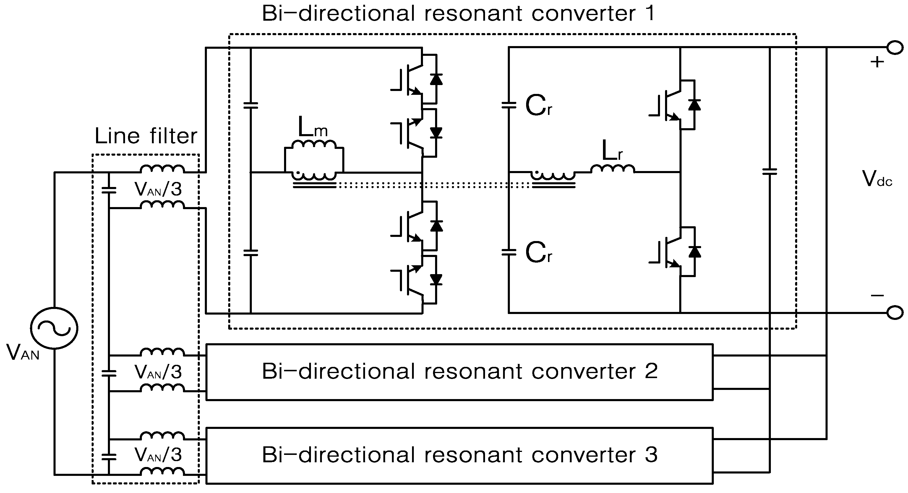
2. Single-Phase Semiconductor Transformer
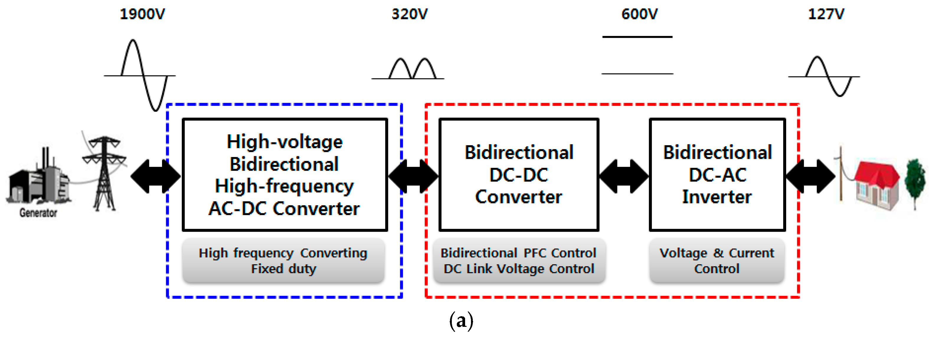
Figure 1 shows the system configuration and operation principle of a single-phase bidirectional semiconductor transformer, which has multiple units of resonant AC–DC converter with insulated gate bipolar transistor (IGBT), hybrid-switching DC–DC converter, and hybrid-switching DC–AC inverter. Three units of half-bridge bidirectional AC–DC converter are series connected on the high-voltage side so that an effective value of 633 V (maximum value of 896 V), which is one-third of the effective value of 1.9 kV, is evenly applied for each unit of AC–DC converters. Three units of AC–DC converter are parallel connected on the low-voltage side so that the effective value of 1.05 A is evenly shared. Each AC–DC converter changes the AC voltage with an effective value of 633 V into the full-wave-rectified waveform with an effective value of 320 V through resonance by a high-frequency transformer. This full-wave-rectified waveform is converted into the DC 600 V by a bidirectional DC–DC converter operated with adjustable duty ratio and hybrid-switching. The DC 600 V is converted into the single-phase AC with an effective value of 127 V by a bidirectional DC–AC inverter that is also operated with hybrid-switching.
The step-down ratio between input and output voltages is primarily determined by the turn ratio of the high-frequency transformer and secondarily determined by the modulation index of the bidirectional DC–AC inverter. The input side of series-connected high-frequency AC–DC converters can have an advantage of easy multiple connections because it can easily form voltage balance. In addition, the entire circuit can be simplified without any additional rectifier by making the converter’s output into the full-wave-rectified waveform. The control of the entire system of a high frequency resonance AC–DC converter is simple because this converter operates at a fixed duty ratio with soft switching and its power factor is controlled through a bidirectional DC–DC converter and a DC–AC inverter.
Table 1 shows the specification of the three-phase semiconductor transformer fabricated as a prototype.
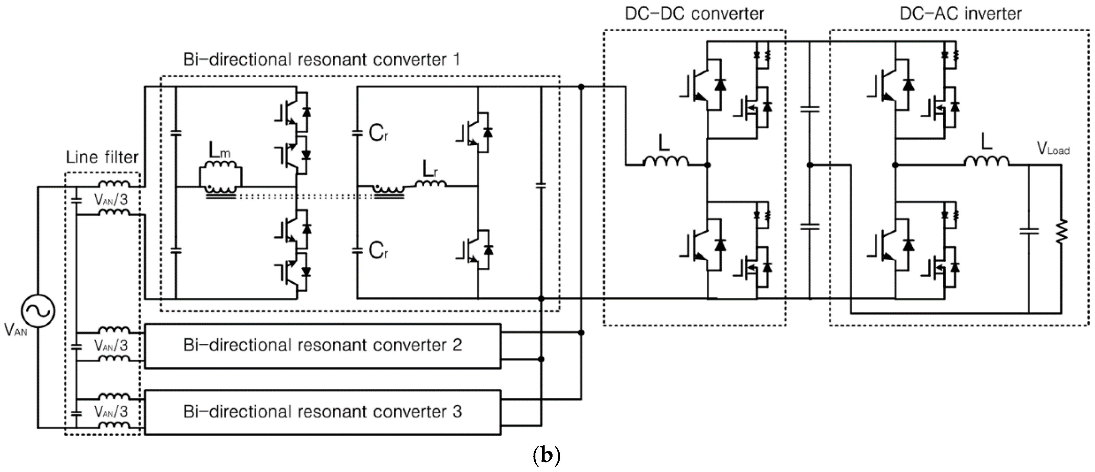
Figure 2 shows the structure of a bidirectional high frequency AC–DC converter that converts single-phase AC 1.9 kV into the 320 V full-wave-rectified waveform. The circuits on the input and output sides are basically configured based on half-bridge units. Three half-bridge units on the input side are series connected because the voltage on the input side is high. Three half-bridge modules on the output side are parallel connected, considering the fact that the voltage on the output side voltage is low. The switching element of the input side of the half-bridge unit was made by connecting two IGBTs in the reverse direction. Bidirectional high-frequency LLC resonant circuit is used to reduce the size of the entire system. The system is operated with lower switching loss because the resonant circuit is operated at a fixed duty ratio [
17].
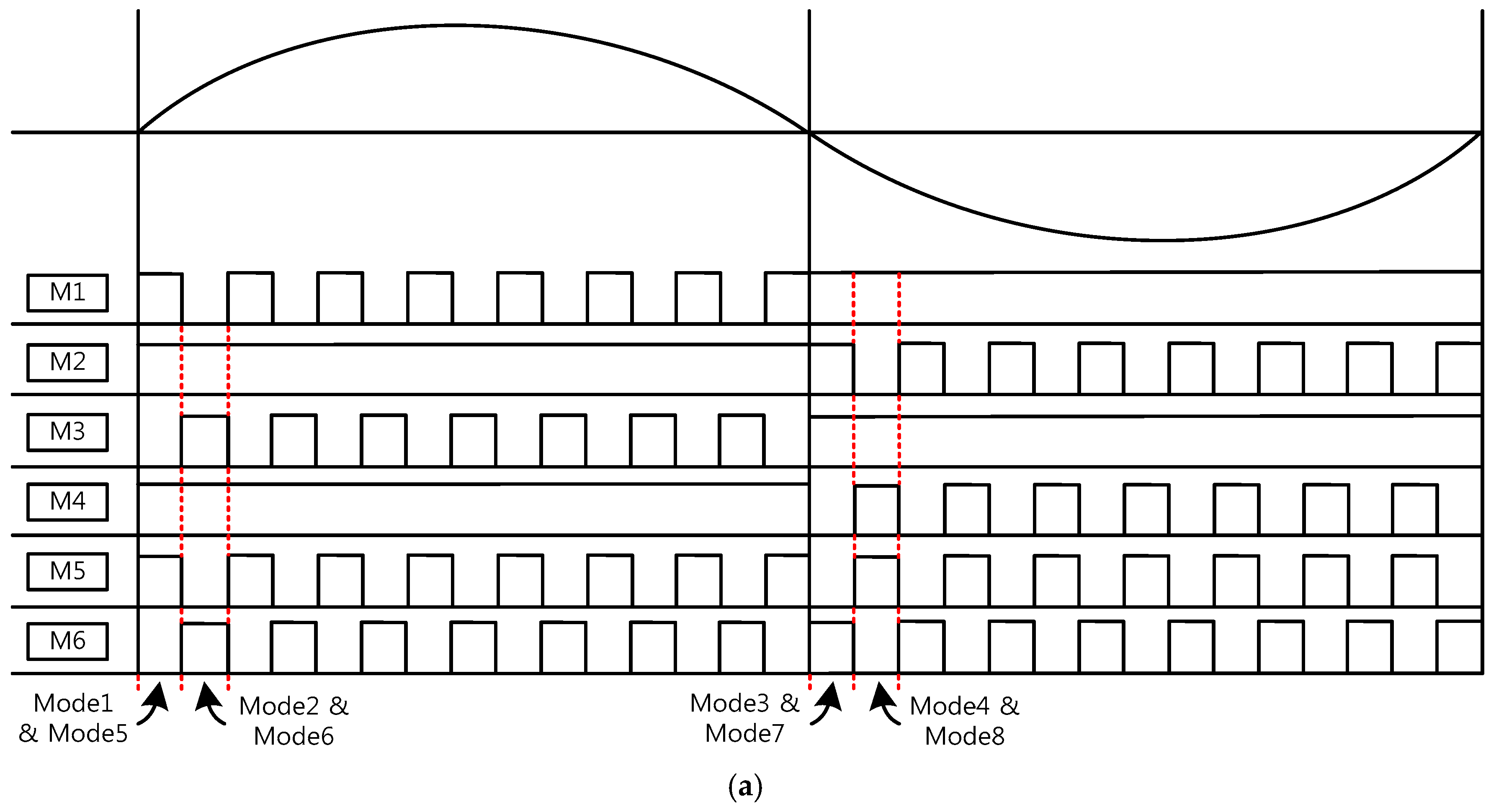
Figure 3a shows the gate pulses supplied to the individual IGBT switch according to the AC input voltage in a single unit of a bidirectional high-frequency AC–DC converter, and where the same gate pulses are generated regardless of power flow direction. Detailed operation modes are described in
Figure 4 and
Figure 5.
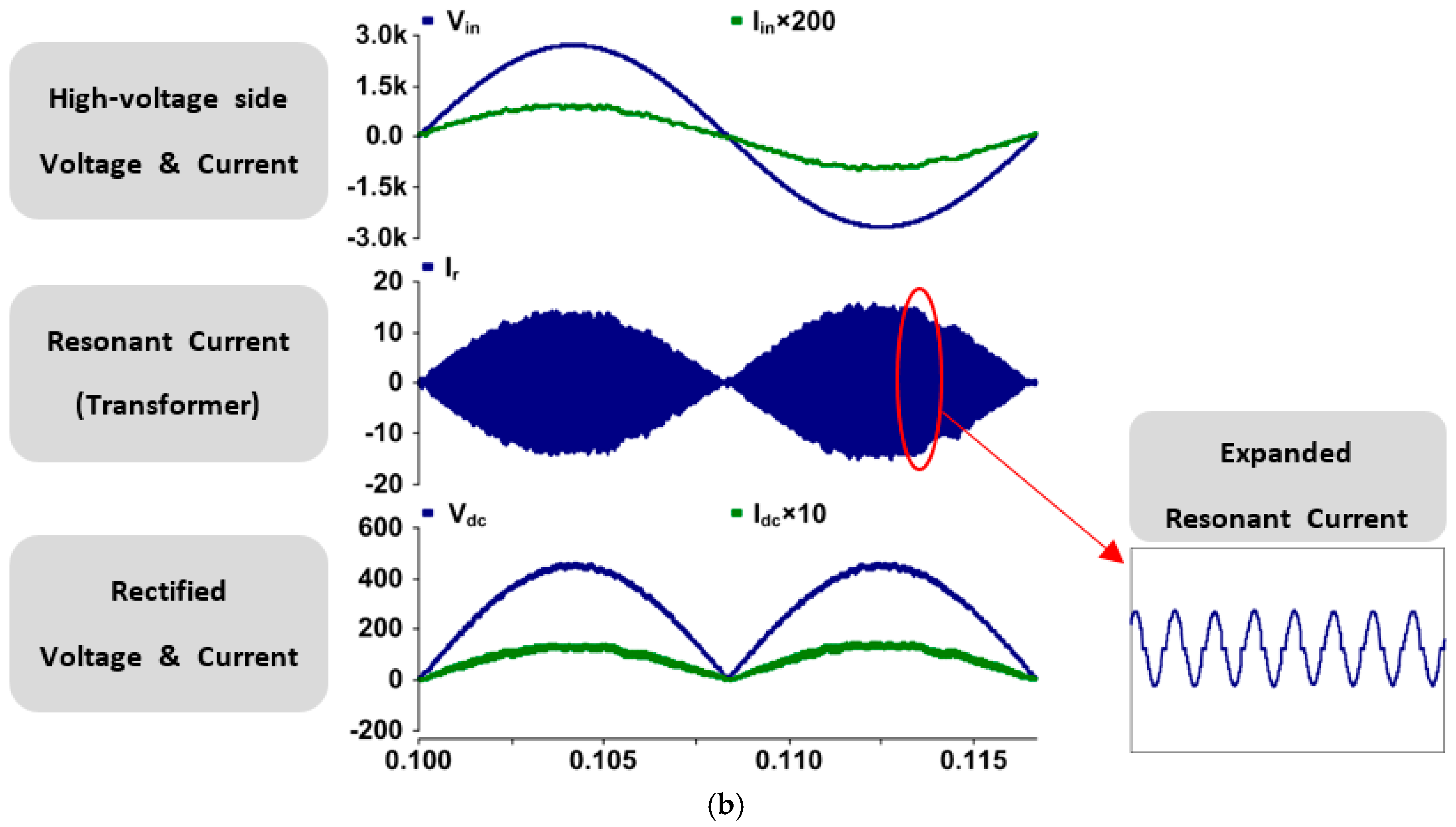
Figure 3b shows the operation analysis results of the proposed AC/DC converter through computer simulations. The upper two waveforms show the input-side voltage and current, which are sinusoidal with negligible distortion. The second waveform describes the resonant current through transformer in which the expanded waveform is shown on the right side. The third two waveforms show the output-side voltage and current, which look like a full-wave rectified shape.
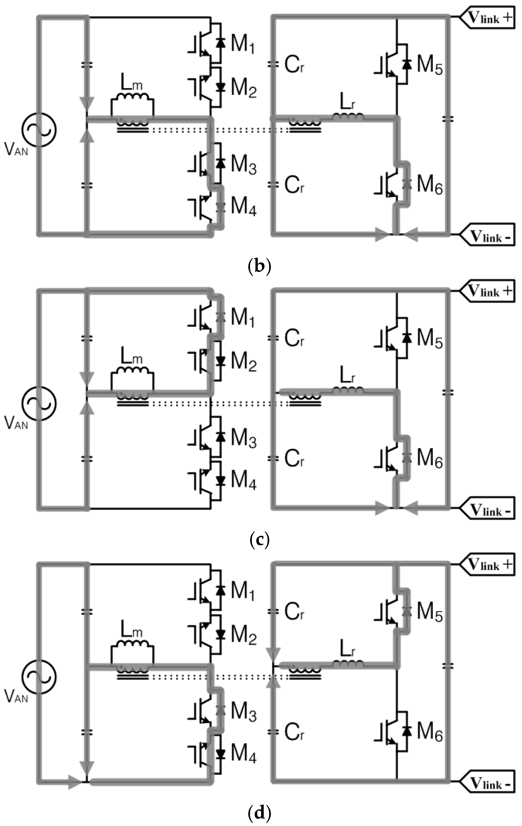
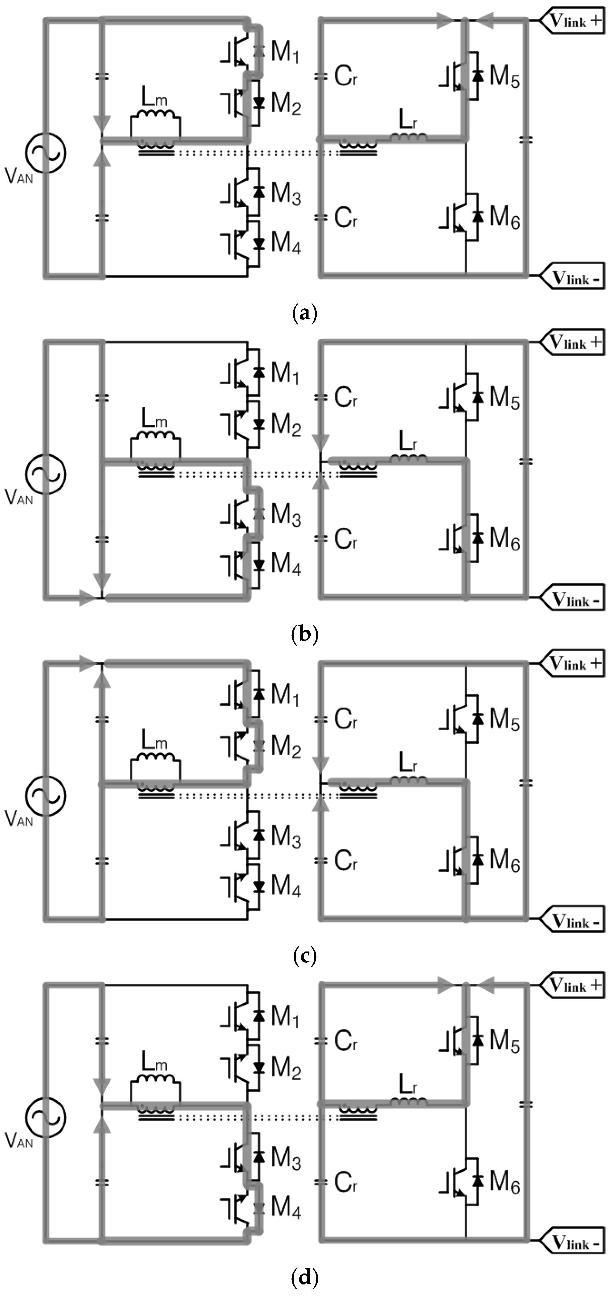
Figure 4 shows equivalent circuits in the forward power flow by each operation mode concentrated on the current path due to the gate driving pulses according to the AC input voltage in
Figure 3. Mode 1 is an equivalent circuit at the positive input voltage as shown in
Figure 4a. The transistor of M1 is turned on and the current that passes through the transistor of M1 and the diode of M2 flows on the primary side of the high-frequency transformer. The current that passes through the diode of M5 flows on the secondary side. Mode 2 is an equivalent circuit at the positive input voltage as shown in
Figure 4b. The transistor of M3 is turned on and the current that passes through the transistor of M3 and the diode of M4 flows on the primary side of the high-frequency transformer. The current that passes through the diode of M6 flows on the secondary side.
Mode 3 is an equivalent circuit at the negative input voltage as shown in
Figure 4c. The transistor of M2 is turned on and the current that passes through the diode of M1 and the transistor of M2 flows on the primary side of the high-frequency transformer. The current that passes through the diode of M6 flows on the secondary side. Mode 4 is an equivalent circuit at the negative input voltage as shown in
Figure 4d. The transistor of M4 is turned on and the current that passes through the diode of M3 and the transistor of M4 flows on the primary side of the high-frequency transformer. The current that passes through the diode of M5 flows on the secondary side.
Figure 5 shows equivalent circuits in the reverse power flow by each operation mode concentrated on the current path due to the gate driving pulses according to the AC input voltage in
Figure 3. Mode 5 is an equivalent circuit at the positive input voltage as shown in
Figure 5a. The transistor of M2 is turned on, and the current that passes through the diode of M1 and the transistor of M2 flows on the primary side of the high-frequency transformer. The current that passes through the transistor of M5 flows on the secondary side. Mode 6 is an equivalent circuit at the positive input voltage as shown in
Figure 5b. The transistor of M4 is turned on and the current that passes through the diode of M3 and the transistor of M4 flows on the primary side of the high-frequency transformer. The current that passes through the transistor of M6 flows on the secondary side.
Mode 7 is an equivalent circuit at the negative input voltage as shown in
Figure 5c. The transistor of M1 is turned on, and the current that passes through the transistor of M1 and the diode of M2 flows on the primary side of the high-frequency transformer. The current that passes through the transistor of M6 flows on the secondary side. Mode 8 is an equivalent circuit at the negative input voltage as shown in
Figure 5d. The transistor of M3 is turned on and the current that passes through the transistor of M3 and the diode of M4 flows on the primary side of the high-frequency transformer. The current that passes through the transistor of M5 flows on the secondary side.
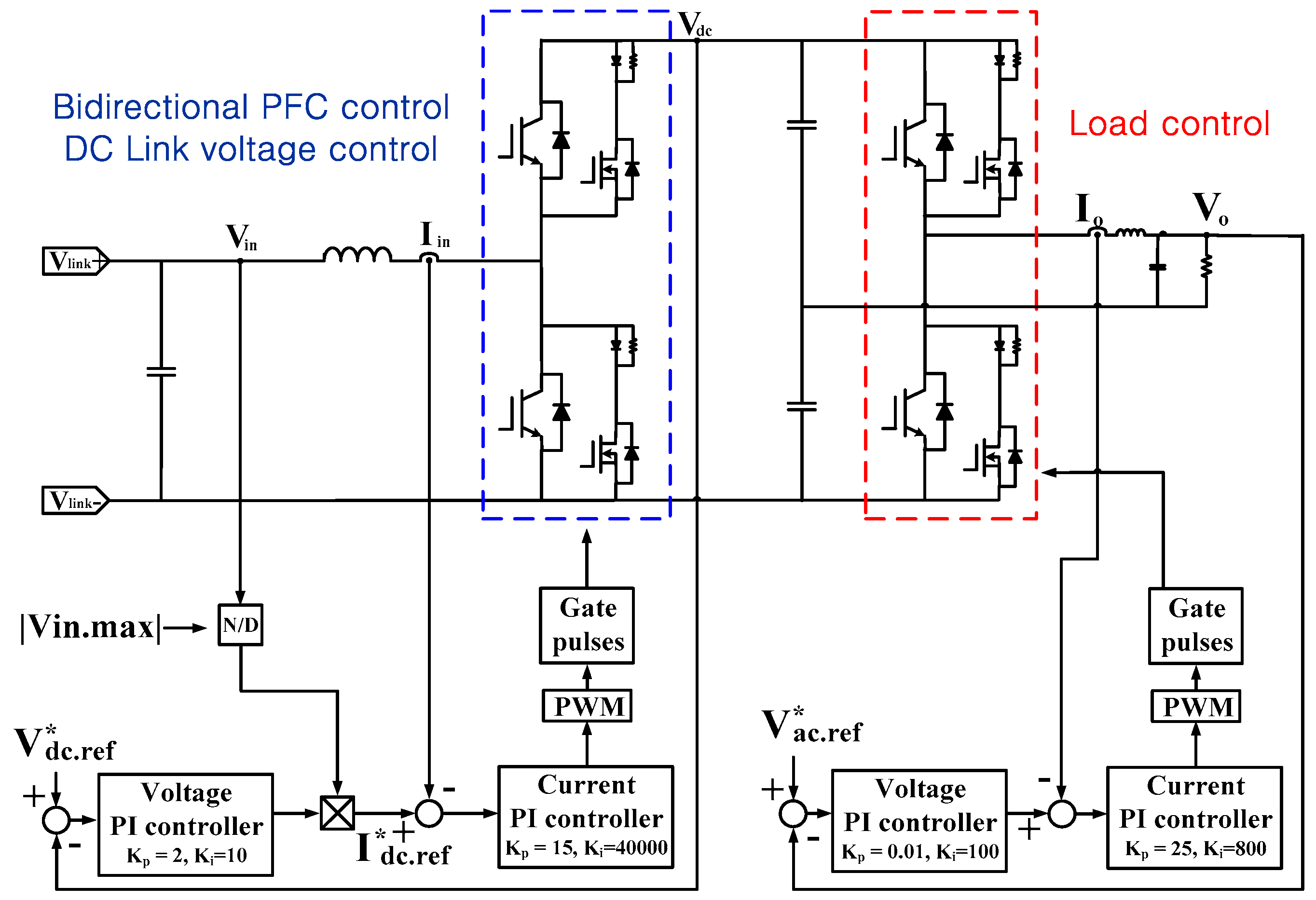
As shown in
Figure 6, a low-voltage side converter has a DC–DC converter that converts the 320 V full-wave-rectified voltage into the 600 V DC voltage, and the DC–AC inverter that converts the DC 600 V into the single-phase 127 V, connected with the DC–DC converter in a two-stage structure. Both DC–DC converter and DC–AC inverter use hybrid switches in which an IGBT and a metal-oxide semiconductor field effect transistor (MOSFET) are parallel connected. The DC–DC converter in the front stage performs power factor control and DC link voltage control, and the DC–AC inverter in the rear stage controls the output voltage supplied to the load.
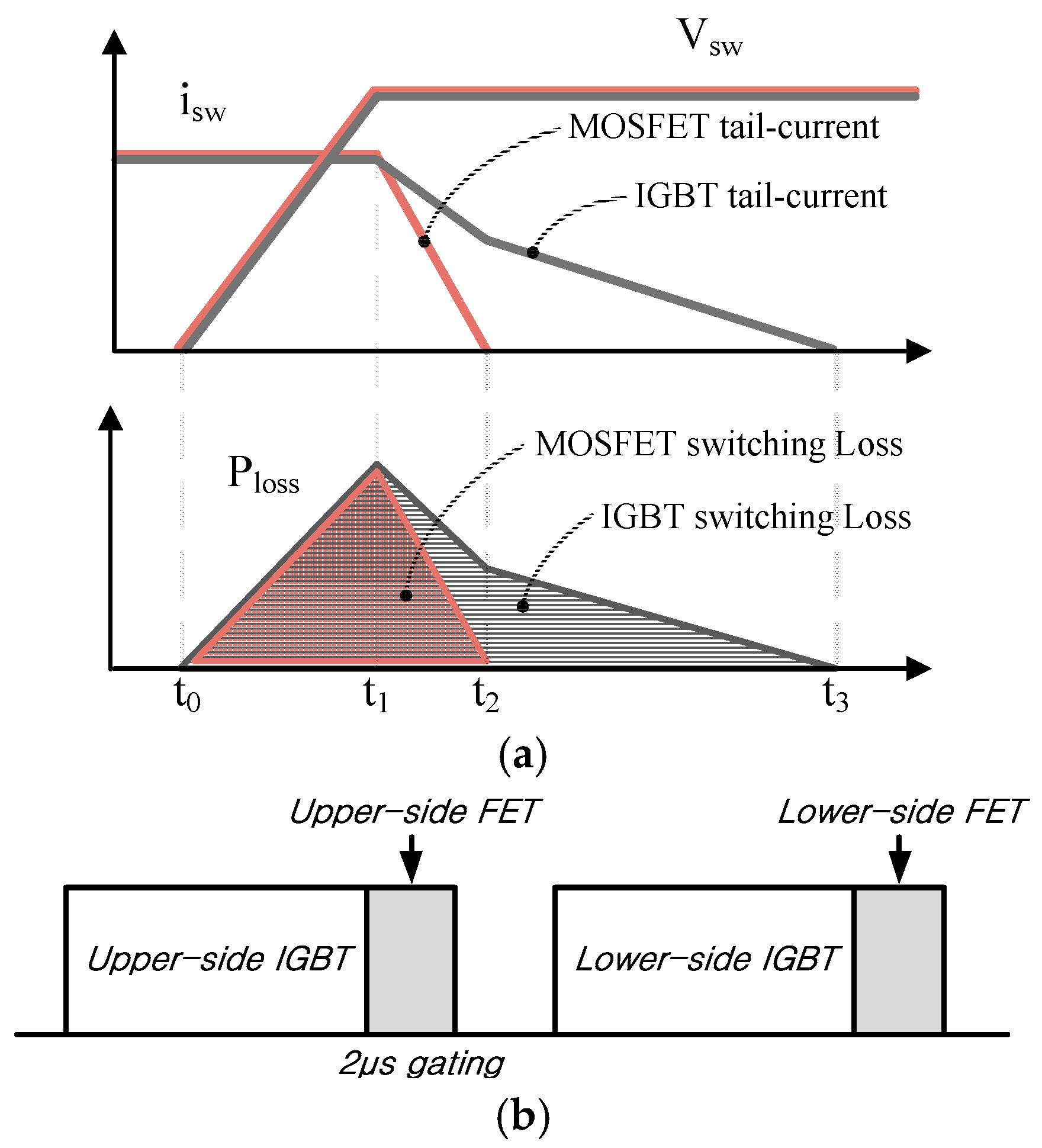
An IGBT has a drawback in that switching loss increases in the turn-off period due to tail-current. As a method of minimizing this disadvantage, a hybrid switch made by parallel-connected IGBT and MOSFET was used [
18,
19,
20].
Figure 7a shows turn-off voltage and current characteristics of IGBT and MOSFET. The tail-current of IGBT subsists for a long time, indicating that relatively larger switching loss is induced in the IGBT compared to the MOSFET.
Figure 7b shows a timing diagram to apply gating signals in hybrid switching. The parallel-connected MOSFET is turned on a little earlier than the time point at which the IGBT should be turned off. The IGBT is turned off thereafter, and the MOSFET is turned off at the time point at which the IGBT is to be turned off. Considering the IGBT tail current, the duration time of MOSFET switching was determined to be 2 μs. In hybrid switching, the inside diode of MOSFET does not have a good reverse recovery characteristic; the additional diode blocks the conduction through the MOSFET body diode. The resistor works to remove the ringing effect during the free-wheeling period that occurs when both IGBT and MOSFET turn off.
3. Computer Simulation
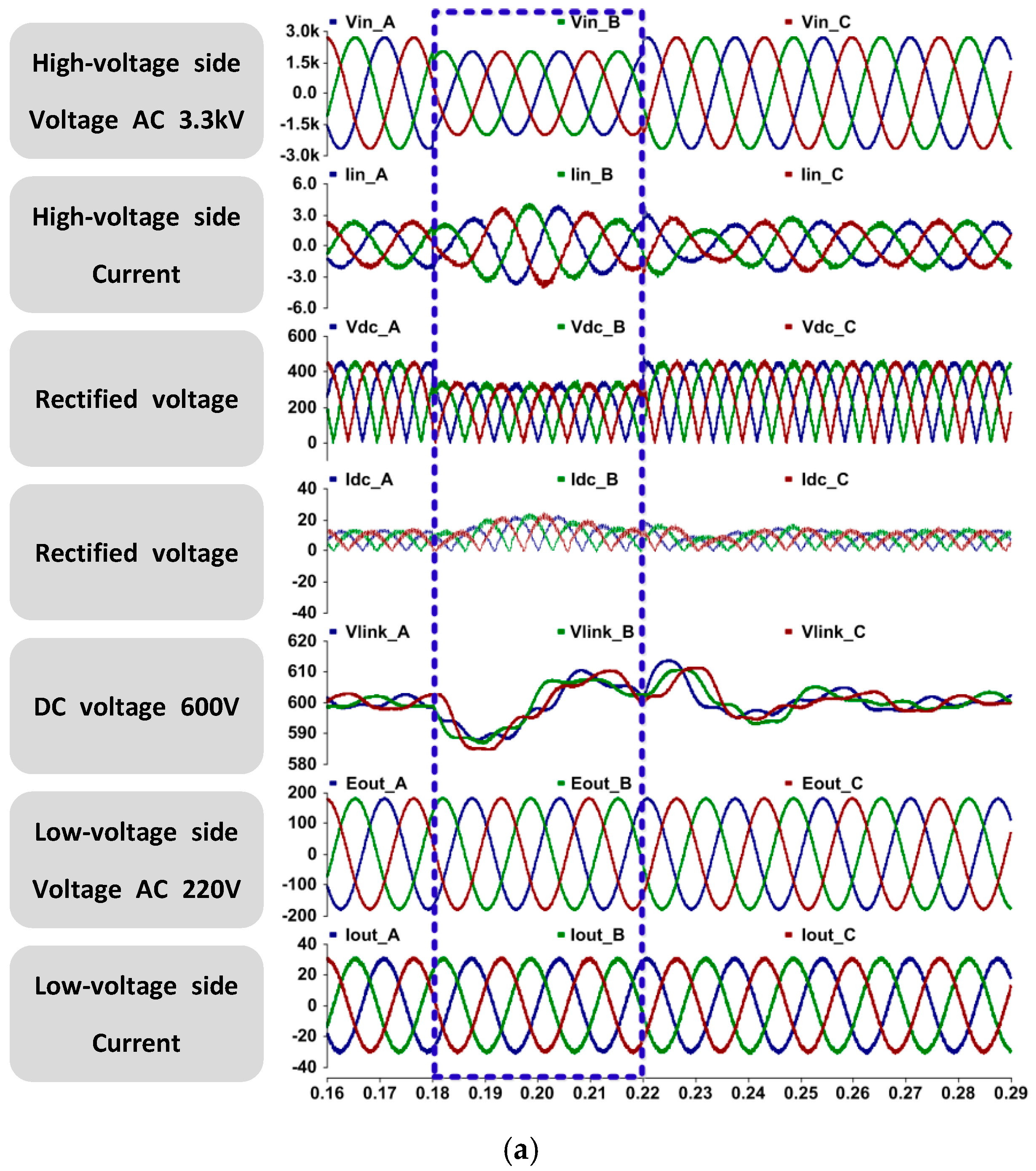
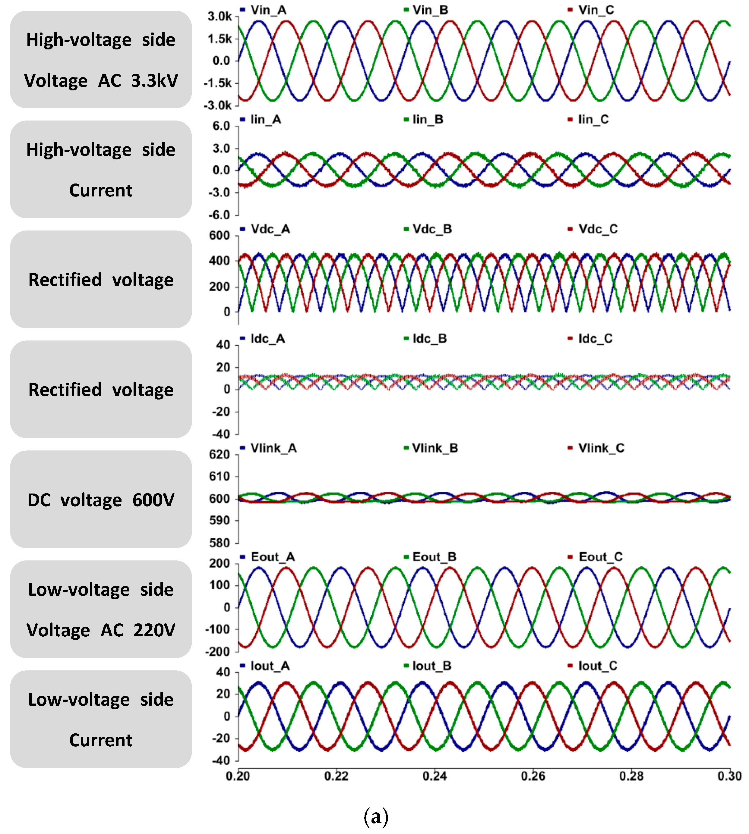
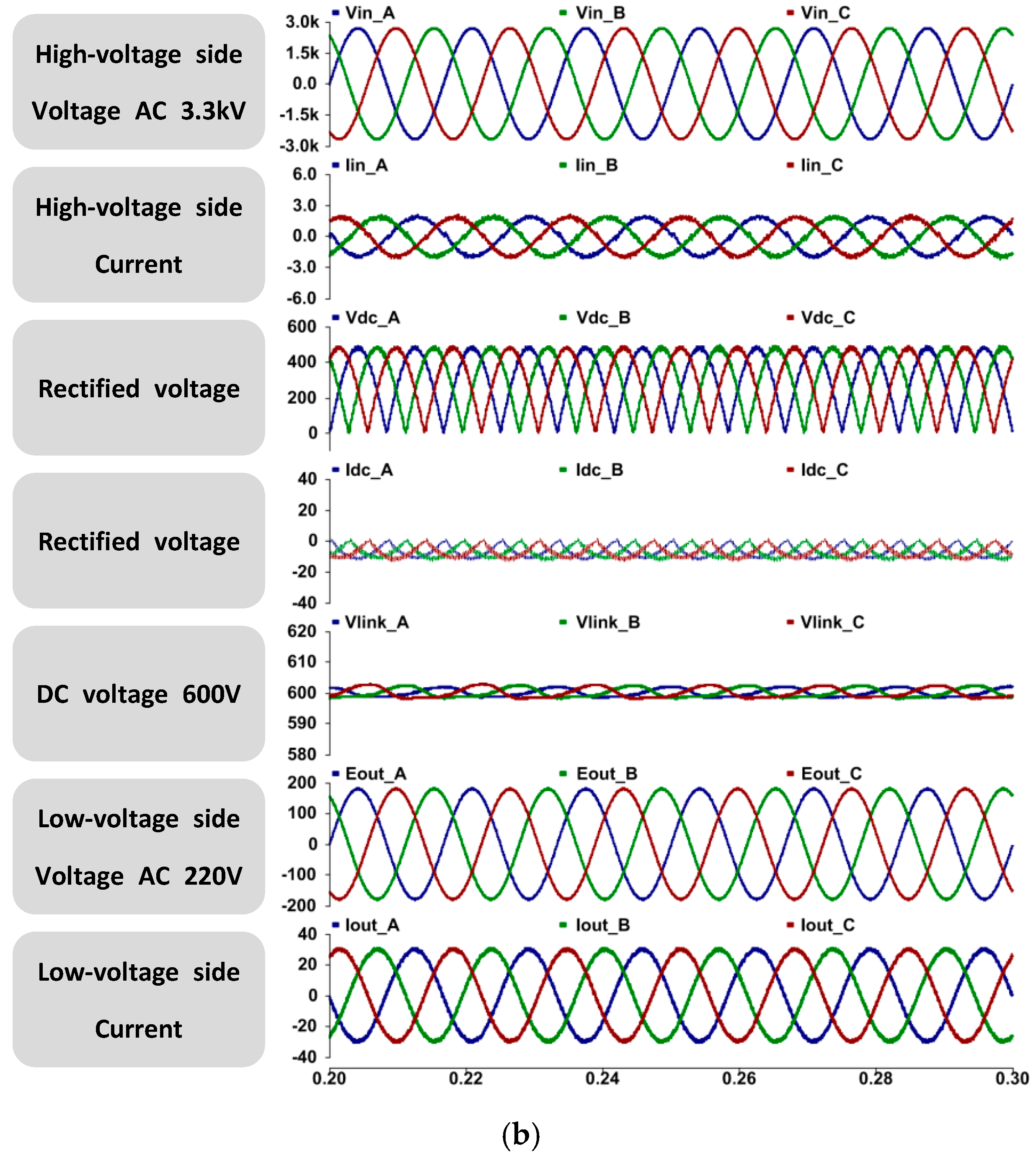
Figure 8 shows simulated waveforms of a three-phase 6 kVA bidirectional intelligent semiconductor transformer.
Figure 8a are the input voltage and current, the rectified voltage and current, the DC link voltage, and the output voltage and current appeared in forward power flow when three-phase 3.3 kV was applied to the high-voltage resonant converter.
Figure 8b shows the same waveforms for the case of reverse power flow.
In these figures, it can be seen that the input voltage and current are in the same phase, indicating that the power factor is corrected and the rectified voltage and current are also in the same phase. The DC link voltage is maintained at 600 V with negligible ripples less than 0.8%, and the output voltage and current waveforms of the DC–AC inverter are sinusoidal with a relatively low level of harmonics.
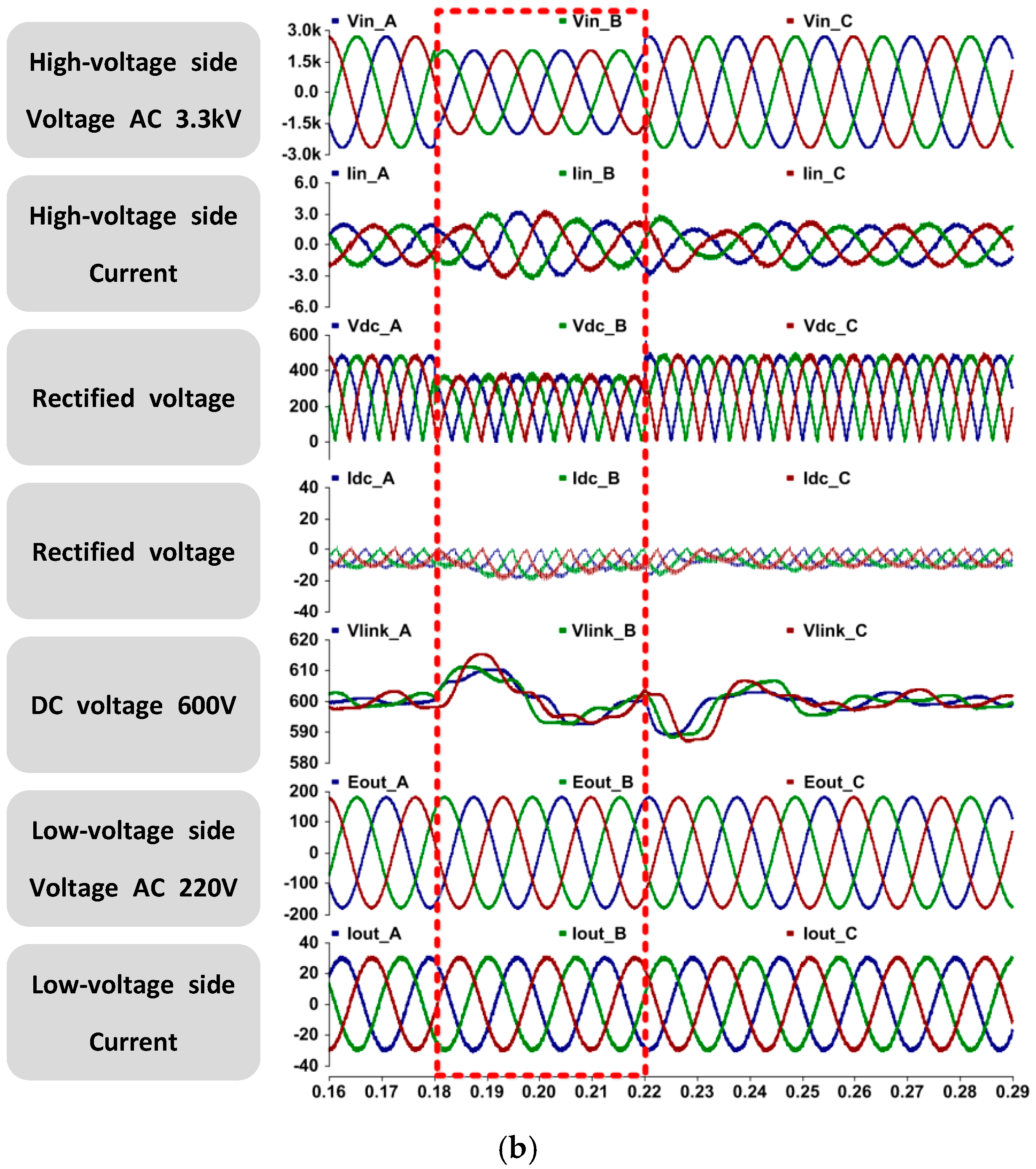
Figure 9 shows the waveforms obtained through simulations conducted to examine circuit operations when sag occurs in the input voltage.
Figure 9a shows the waveforms of the circuit operation in the case of forward power flow and
Figure 9b shows the waveforms of the circuit operation in the case of reverse power flow. It can be seen that when sag occurs, the rectified voltage becomes lower and the current increases in order to supply constant power to the output side. However, the DC voltage is maintained at 600 V through the voltage control of the DC–DC converter. It can also be seen that the output voltage and current are maintained at constant values regardless of the sag, even though the voltage ripple is 2.5%, which is higher than the ripple of 0.8% in normal operation.
4. Hardware Experiment
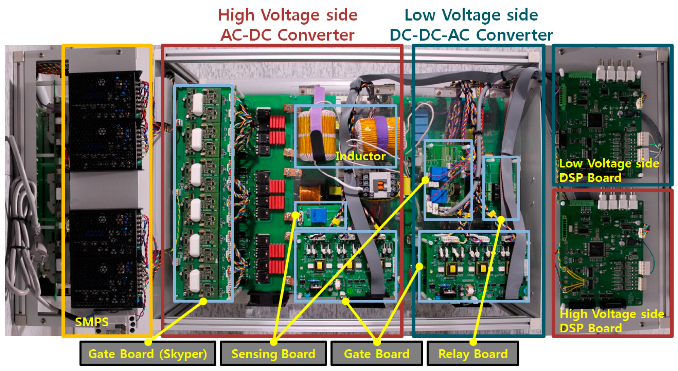
Figure 10 shows a prototype of single-phase semiconductor transformer with a rating of 1.9 kV/127 V 2 kVA that was fabricated and experimented on in the lab. A prototype of three-phase semiconductor transformer with a rating of 3.3 kV/220 V 6 kVA was fabricated by coupling three single-phase units in Y-connection and mounted in a rack as shown in
Figure 10. The input voltage and current, rectified voltage and current, DC link voltage on the high-voltage side, and the voltage and current on the low-voltage side were measured in real time and indicated on the top of the rack for monitoring purpose.
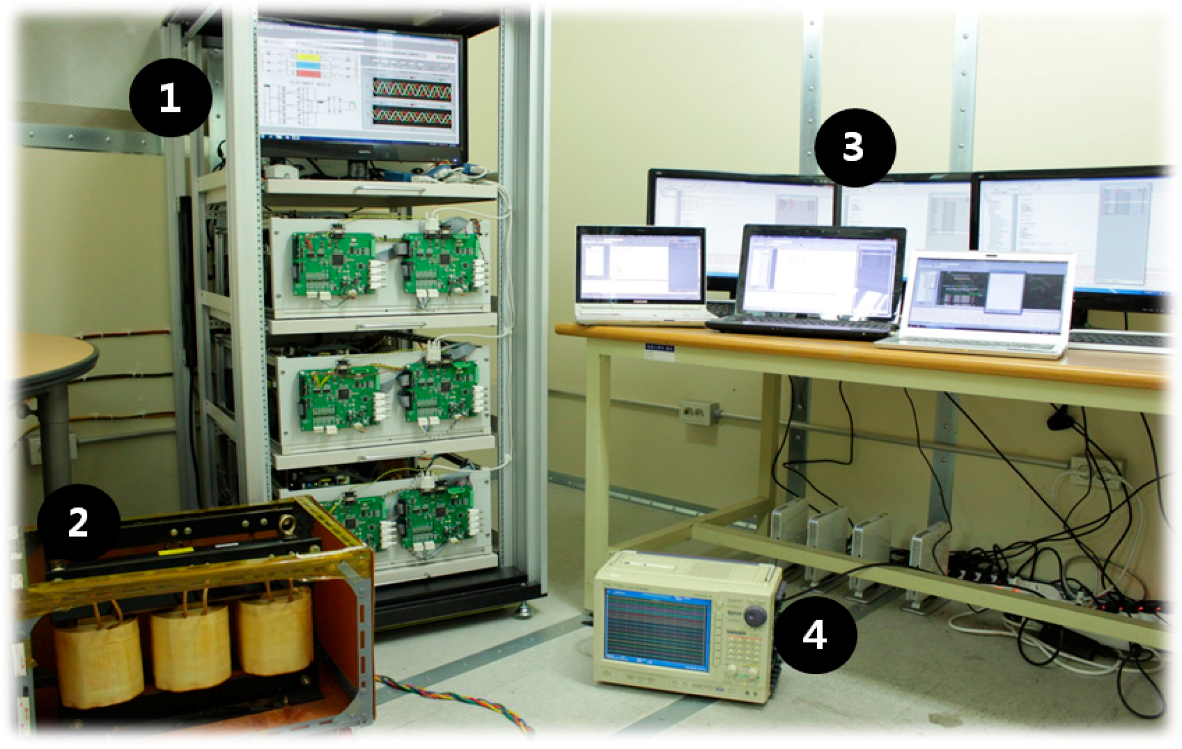
Figure 11 shows a configuration of the entire experimental set-up for analyzing the operation characteristics of the three-phase 3.3 kV/220 V 6 kVA semiconductor transformer.
① is the three-phase semiconductor transformer fabricated in the laboratory. Y-connected three units of single-phase semiconductor transformer are mounted on the lower part and a monitoring system is mounted on the upper part; ② is a conventional 380 V/3.3 kV three-phase four-wire transformer for supplying 3.3 kV power to the semiconductor transformer; ③ is the main PC and three notebooks necessary to download control algorithms programmed with C code for the DSP boards, which are mounted on each single-phase semiconductor transformer; ④ is a 16-channel oscilloscope frequently used for measurements that enables checking whether the data obtained from DSP boards and LabView are accurate.
The designed monitoring system based on LabView should display at least six items of information including the input voltage and current, rectified voltage and current, and output voltage and current of the semiconductor transformer. If three-phase operation is involved, it should display at least 18 items of information. So, curve-fitting technique was utilized to display all the data on the monitoring screen.
Since the DSP board currently being used in the lab does not have enough pulse width modulation (PWM) channels, each single-phase semiconductor transformer has two DSP boards for the high-voltage side and the low-voltage side, respectively. For control and monitoring purposes, two DSP boards in a single-phase semiconductor transformer should be connected through CAN communication. One DSP board in a single-phase semiconductor transformer transmits data to LabVIEW through CAN communication.
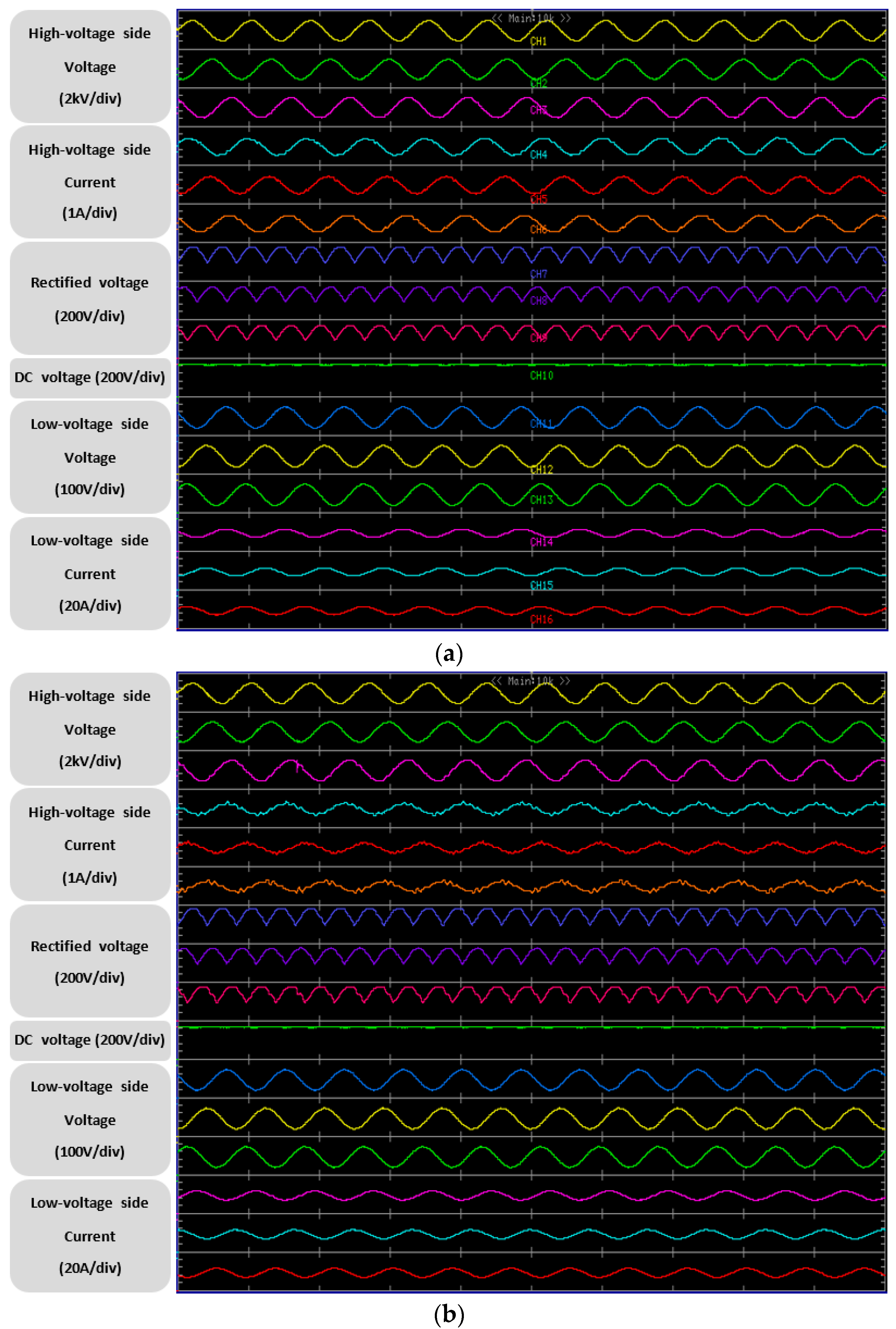
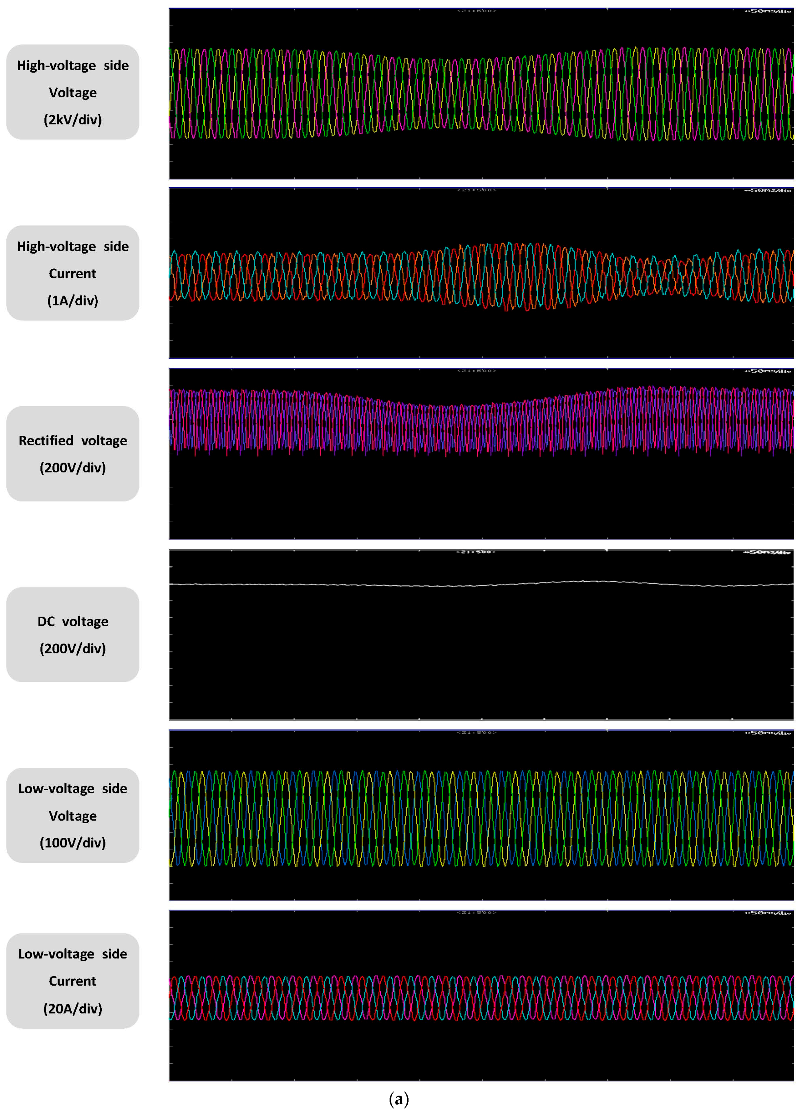
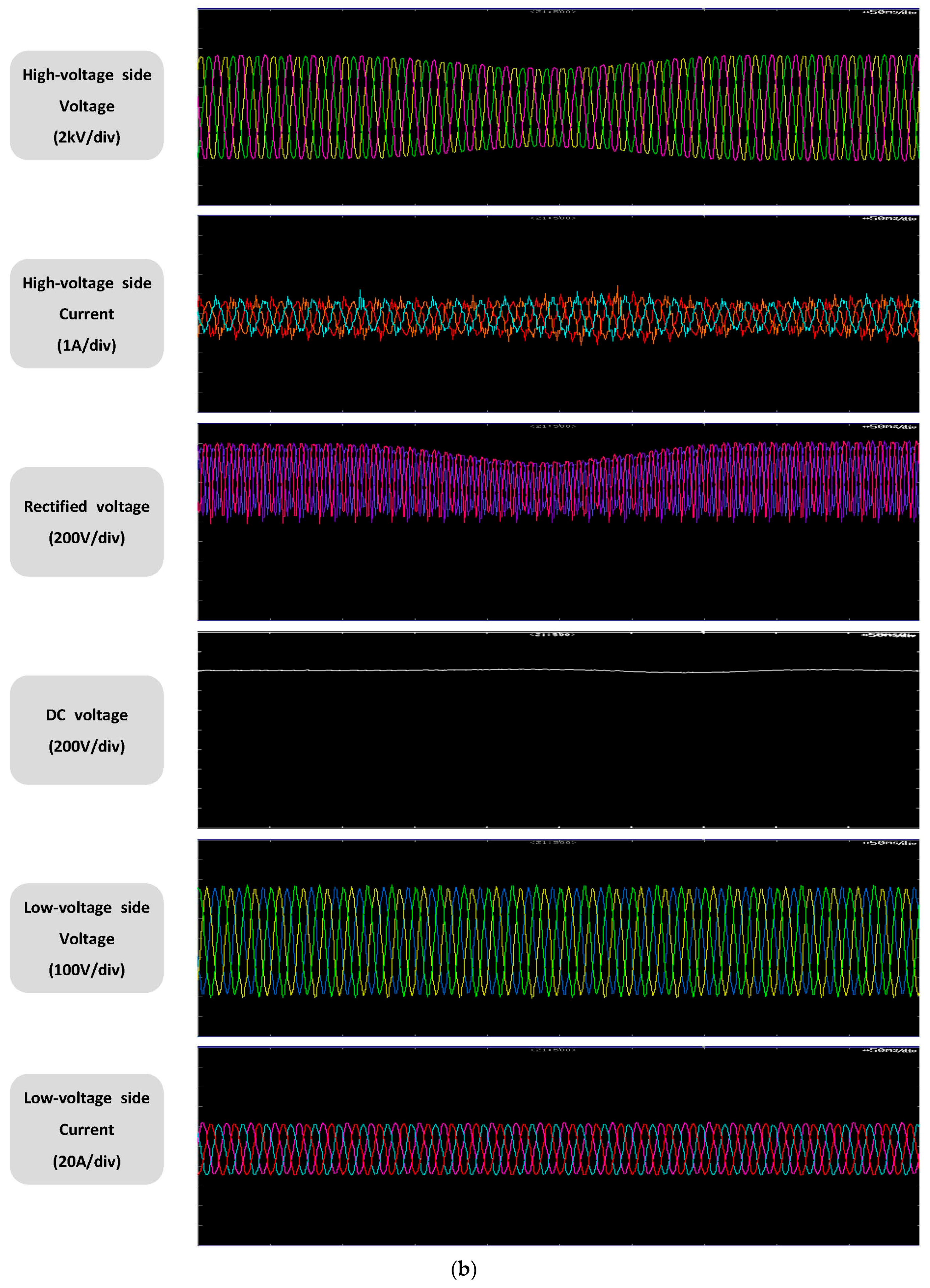
Figure 12 shows the experimental waveforms of a three-phase 6 kVA bidirectional intelligent semiconductor transformer. The waveforms in
Figure 12a are the three-phase input voltage and current, three-phase rectified voltage and current, DC link voltage, and three-phase output voltage and current in forward power flow when three-phase 3.3 kV was applied to a high-voltage side of resonant converter. The waveforms in
Figure 12b are for the case of reverse power flow.
In these figures, it can be seen that the input voltage and current are in the same phase, indicating that the power factor is corrected and the rectified voltage and current are also in the same phase. The DC link voltage is maintained at 600 V with negligible ripples, and the output voltage and current of the DC–AC inverter are sinusoidal with relatively low level of harmonics. These experimental results are consistent with the simulation results shown in
Figure 8.
Figure 13 shows the waveforms obtained through simulations conducted to examine circuit operations when sag occurs in the input voltage.
Figure 13a shows the waveforms from the circuit operation in the case of forward power flow.
Figure 13b shows the waveforms from the circuit operation in the case of reverse power flow. It can be seen that when sag occurs, in order to supply constant power to the output side, the rectified voltage becomes lower and the current increases. However, the DC voltage is maintained at 600 V through the voltage control of the DC–DC converter. It can also be seen that the output voltage and current are maintained at constant values regardless of the input voltage sag. The above results obtained through experiments are consistent with the simulation results shown in
Figure 9.
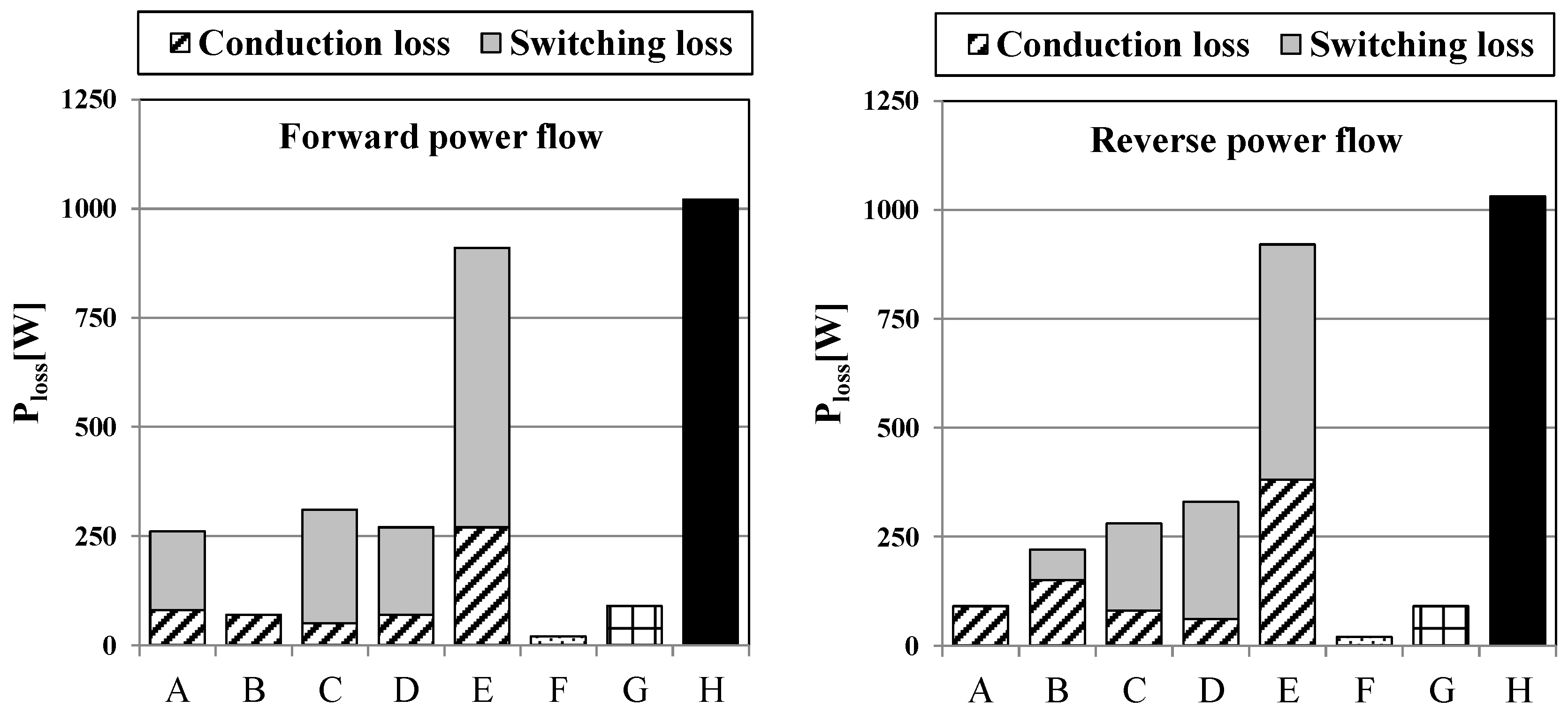
The entire efficiency of a 6 kVA three-phase semiconductor transformer was measured using a power analyzer, which shows approximately 83% in both forward and reverse power flows.
Figure 14 shows loss analysis results according to bidirectional power flow, where “A” shows total losses in the primary side of high-voltage AC–DC converter, “B” shows total losses in the secondary side of high-voltage AC–DC converter, “C” shows total losses of the DC–DC converter, “D” shows total losses of the DC–AC inverter, “E” shows total losses (adding A, B, C, and D), “F” shows the transformer loss, “G” shows the inductor loss, and “H” shows entire losses of the semiconductor transformer (adding E, F, and G). The switching losses of the high-voltage AC–DC converter, and the DC–DC converter and DC–AC inverter are dominant due to high switching frequency.
5. Conclusions
This paper describes experimental results of a prototype of a three-phase 3.3 kV/220 V 6 kVA bidirectional semiconductor transformers to analyze its performance. The prototype was configured by Y-connection of three units of single-phase 1.9 kV/127 V semiconductor transformer.
Each single-phase unit has three units of bidirectional half-bridge high-frequency resonant AC–DC converter, one hybrid-switching bidirectional DC–DC converter, and one hybrid-switching bidirectional DC–AC inverter. Three units of half-bridge high-frequency resonant AC–DC converter are series connected on the high-voltage side to evenly divide the input voltage into thirds, and are parallel connected on the low-voltage side to increase the current. A hybrid-switching scheme was utilized to reduce the switching loss in the DC–DC converter and the DC–AC inverter. In order to monitor the entire system operation, DSP boards and PCs were connected with CAN communication based on LabView to create a display system to indicate the input voltage and current, rectified voltage and current, and output voltage and current.
Through the results of diverse experiments, it could be seen that the developed three-phase semiconductor transformer operated properly during normal operation and under input voltage sag. However, the system efficiency is rather lower at approximately 83%. Therefore, the system efficiency should be enhanced to at least 90% by adopting optimum designs and replacing the existing IGBT with a new switching device such as an SiC device.
The fabricated prototype of a three-phase semiconductor transformer confirms the possibility of commercialization with a higher voltage rating by increasing the number of converter units connected in series at high-voltage side and in parallel at low-voltage side. In addition the proposed three-phase semiconductor transformer has advantages in fabrication and maintenance because it is designed with a modular structure.


