Article

Partial Discharge Measurement under an Oscillating Switching Impulse: A Potential Supplement to the Conventional Insulation Examination in the Field

State Key Laboratory of Electrical Insulation for Power Equipment, Xi’an Jiaotong University, Xi’an 710049, China
*
Authors to whom correspondence should be addressed.
Energies 2016, 9(8), 623; https://doi.org/10.3390/en9080623
Submission received: 14 June 2016 / Revised: 27 July 2016 / Accepted: 1 August 2016 / Published: 9 August 2016

Abstract

:
Partial discharge (PD) detection under oscillating switching impulse (OSI) voltage was performed on three types of insulation defects, including a protrusion on a conductor, a particle on an insulator surface, and a void in an insulator, which are three kinds of the common potential insulation hazards in gas insulated power apparatus. Experiment indicated that the PD sequences under OSI were composed of various combinations of the single pulse, the multiple pulses, and the reverse polarity pulse. The difference between the PD inception voltage (PDIV) and the breakdown voltage (BDV) under OSI voltage was greater than that under alternating current (AC) voltage in some cases, which can provide a more sufficient margin below the BDV for PD diagnosis. The OSI voltage also showed a better performance for exciting PDs with detectable magnitudes from small-scale defects, of which the AC voltage was incapable under our test conditions. The different PD activities with different interfaces under an impulse and a slowly varying voltage were speculated to be associated with the gradient of the background electric field and the space-charge mobility.

Graphical Abstract

1. Introduction

Partial discharge (PD) detection has been widely used in the quality control of high-voltage power apparatus serving a power system, by which the overall insulation status and local condition are expected to be examined during routine tests, handing over tests and even field tests. An AC withstand test combined with PD detection has become a compulsory test during delivery, especially for an ultrahigh-voltage gas-insulated switchgear or a transmission line. The insulation defects are caused by manufacturing errors at the factory as well as transportation and assembly in the field. Thus, a short-time AC resonant withstand test needs to be implemented after assembly and repair, and a PD test is also applied in an effort to determine any unknown damage. Aside from these tests, some online diagnostic techniques, particularly the ultrahigh frequency (UHF) method and acoustical wave (AE) method [1], have been developed to avoid insulation failure during operation. Admittedly, these offline and online methods have served irreplaceable roles in insulation diagnosis for many years. However, practical experience and studies have shown that the AC PD test is probably not a universal solution for finding all types of insulation defects, especially for conductive protrusions and particles on the insulator surface. This problem is supposed to be subject to diffusion-limited charge accumulation, which confines the discharge intensity to an undetectable level [2,3]. Some hidden defects are hardly exposed by the AC voltage field test and can continuously deteriorate the insulation and shorten the service life of the equipment prior to failure. An increasing number of failures have occurred prior to the end of the designed service life. In this case, the impulse voltage test is expected to be an effective supplement to an insulation quality examination in the field because of its high-field effect and limited destructiveness. To address the inconvenience due to the low delivery efficiency of the impulse generator, the IEC 60060-3 standard recommends oscillating impulse voltages as alternatives to aperiodic impulses, which are more feasible in a field test [4]. Figure 1 shows an ongoing oscillating impulse withstand test of a gas-insulated switchgear in the field.
Thus, PD detection could be simultaneously performed with withstand tests to exclude the critical defects arising from transportation and assembly [5]. In the past few decades, the gap breakdown in stressed SF6 gas under impulse conditions has been extensively studied [6,7,8]. Relevant theories based on the streamer and leader mechanisms have been developed by experiments [9] and simulations [10,11]. The aims of most of these previous studies were the design of the power equipment and the failure mechanisms of the SF6 insulation. The PDs under impulse conditions were generally thought to be phenomena occurring in the initial stage of breakdown and seldom studied in terms of insulation diagnosis. Further, we have previously investigated the PD characteristics and impact factors under lightning and switching impulses for various artificial defects in SF6 gas [12,13].
On the basis of previous studies, this paper summarizes the PDs under impulse voltages from the viewpoint of insulation diagnosis in practice. The PD behaviors under an oscillating switching impulse (OSI) are described by exemplifying the typical PD sequences and PD pulses caused by different defects. The effectiveness of various voltages including the switching impulse (SI), oscillating switching impulse (OSI), and AC voltages on the PD diagnosis is quantitatively compared. The reasons for the different PD activities under an impulse and a slowly varying voltage are discussed, and they are speculated to be associated with the field-dependent stabilization effect.

2. Experimental Setup

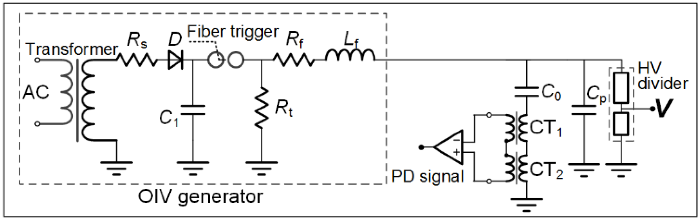
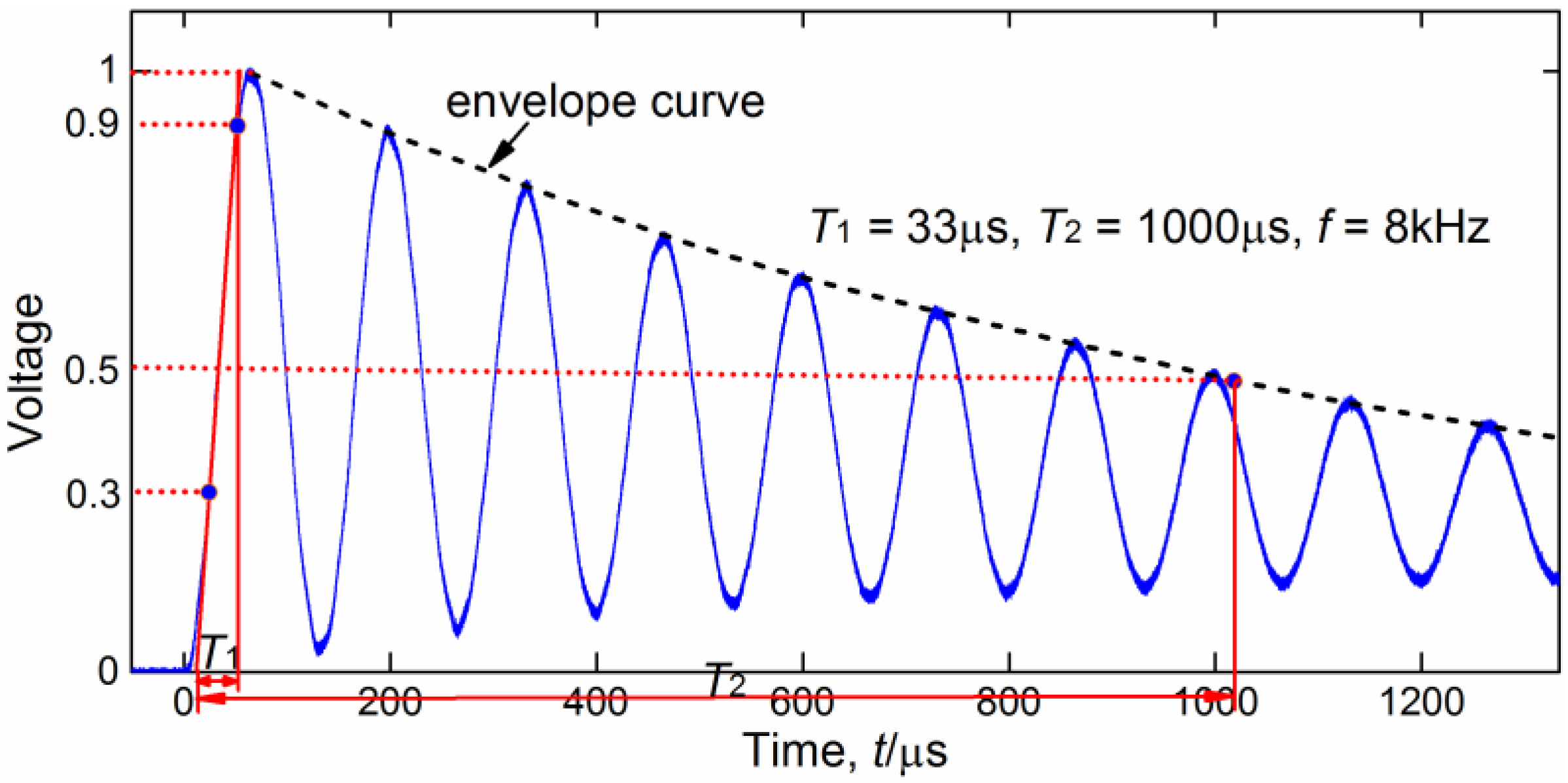
2.1. Partial Discharge (PD) Measurement under Impulse Conditions

Under surge voltage conditions, one difficult problem in PD detection is the separation of PD signals with a magnitude on the order of approximately a few milliamperes from the great capacitive displacement flow on the order of approximately a few amperes. For example, a 65 kV oscillating lightning impulse (OLI) voltage applied to a test object with a capacitance of 75 pF could produce a displacement current above 2 A, as shown in Figure 2.
To address this problem, a capacitor could be employed as the balance bridge in parallel with the test object [14]. This method is effective for the capacitive specimen under an AC voltage but unsatisfactory under impulse conditions because the equivalent circuit is no longer a lumped-parameter circuit but distributed. Moreover, it is also difficult to obtain the equivalent parameters for each specific condition, especially in a field test. Another approach is to filter the surge flow that occupies the relatively low frequency range by introducing a second-order RC filtering circuit at the front of the preamplifier, as shown in Figure 3. However, this approach gives rise to a serious decrease in the sensitivity for PD detection due to the large ratio of the surge amplitude in the low-frequency range to the PD magnitude at a high frequency. In this study, a feasible PD detection circuit was applied under impulse conditions, as shown in Figure 3. Signal coupling is realized by two current transformers (CTs), both of which were placed around the ground pillars. One wideband CT (CT1, 20 kHz–110 MHz, 5 V/A, IPC-CM-500) responds to the total transient signal over a wide frequency range covering the displacement-current and PD signals. CT2 was a homemade CT (3 kHz–1.7 MHz, 5 V/A), which only responds to the displacement-current signal in the low-frequency range. By subtracting the output of CT2 from that of CT1 with a differential amplifier, most of the displacement component in the total current signal could be canceled. Finally, the output of the differential module was processed by a high-pass filter to separate the PDs from the residual displacement current. A CT could be employed for impulse PD detection because it can quantify the severity of the PD and can be conveniently installed on power equipment without contact. The sensitivities of the measurement systems for the impulse PD and AC PD can be verified by calibration, and their minimum detectable levels are 5 pC and 2.0 pC, respectively. The simplified circuit of the oscillating impulse generator used in the experiment is shown in the dotted box in Figure 4, by which OSI voltage (33/1000 μs, 8 kHz) can be produced. The waveform of the OSI voltage is shown in Figure 5.

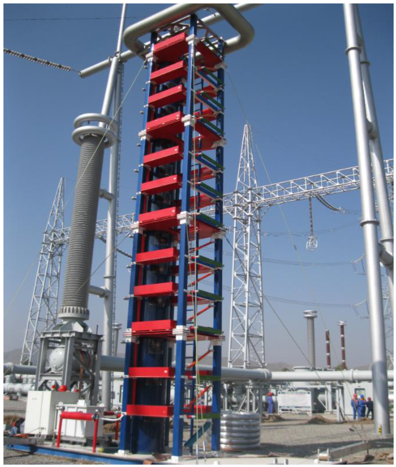
2.2. Artificial Defect Models and Experimental Setup
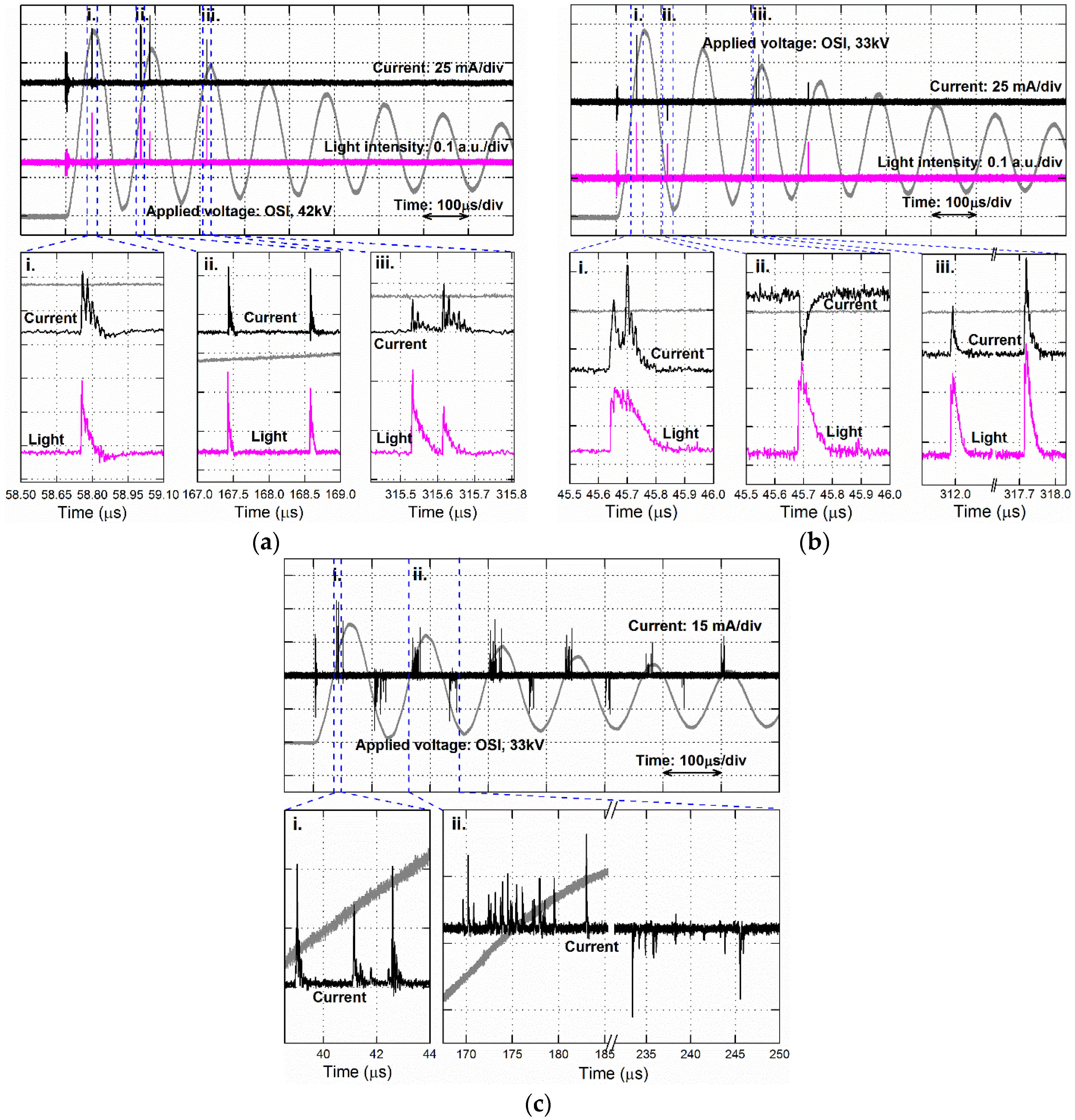
In our experiment, a stainless-steel test chamber that could withstand a gas pressure up to 0.7 MPa and applied voltages up to 150 kV (50 Hz AC peak) was used to build a SF6 gas insulated system, as shown in Figure 6a. Any specific insulation system may contain some insulation defects, which arise from the design, manufacturing, assembling, and service stress history. According to the nature of the two or three major dielectric boundaries, the insulation defects could be classified and simplified into small-scale defect models which can be used in experimental studies. Considering the contribution of the electric field to the excitation of the PDs, three defect models including a metal protrusion (see Figure 6b), a metal particle (a metal needle was employed as the particle) on an insulator surface (see Figure 6c), and a gaseous void in an insulator (see Figure 6d) were developed to simulate the defects with different dielectric interfaces. In our test, all the defect models were placed in a pair of parallel plate copper electrodes which can provide a uniform background electric field. The protrusion defects (as shown in Figure 6b,c) were made of stainless steel (Crl8Ni9Ti). To make the void defect model (see Figure 6d), two epoxy resin plates, each with an artificial pitting at the center, were spliced face to face by using a mixture of E51 epoxy resin (Deyuan Epoxy Resin Co., Ltd., Feicheng, China) and 10% DDS curing agent (Jianxin Imp & Exp Co., Ltd., Cangzhou, China). To ensure a good contact between the electrode and the epoxy resin without gas gap, the electrode was also spliced to the epoxy resin plate which has a void inside. After splicing, the defect samples were kept in a vacuum oven at 55 °C for over 24 h for drying. The relative dielectric constant of the E51 and DDS mixture was 4.1–4.3, which is consistent with that of the epoxy resin block. The scale of the artificial defect was controlled by the parameters listed in Table 1.
The overall configuration of the PD detection system is shown in Figure 7. The PD signals are recorded by a digital oscilloscope (DSO, LeCroy 64Xs-B, Teledyne LeCroy, Chestnut Ridge, NY, USA), sampling rate 10 Gs/s; analog bandwidth 600 MHz). To avoid electromagnetic (EM) interference, metal armored double-shielded measurement cables were used for signal transmission. All recording apparatus were placed in an EM-shielded room. The voltage divider used in the test had a response time less than 100ns and a measurement range up to 150 kV. The coupling capacitance value in parallel with the test object was 1000 pF. A photomultiplier tube (PMT, R7600U, Hamamatsu, Japan), response over a wavelength range of 300–850 nm) for optical detection was placed behind the observation window of the chamber and employed to assist with the PD current measurement. The optical windows of the chamber were constructed of synthetic fused silica glass (above 85% transmittance from 175 nm onward and 90% from 220 nm onward).
In our test, the PD inception voltages (PDIVs) under OSI and AC voltages were determined by step-up voltage method. The amplitude of the OSI was controlled by the output of the charging transformer of the Marx generator. The same test procedure was repeated on the same test object until that the PD current pulses or light pulses were detected for 5 times for every 10 tests at a certain voltage which was identified as the fifty probability PDIV (abbr. PDIV50%). The same method was applied to determine BDVs under AC and OSI voltages. To investigate the PD activity under the equivalent voltage levels but different voltage types, the predetermined PDIVs were used as the benchmarks of the applied voltage level (e.g., 1.1 times PDIV (abbr. 1.1PDIV), 1.2 times PDIV (1.2 PDIV) and so on). Considering the influence of the residual space charge, the time interval between two tests was kept above 5 min.

3. Results

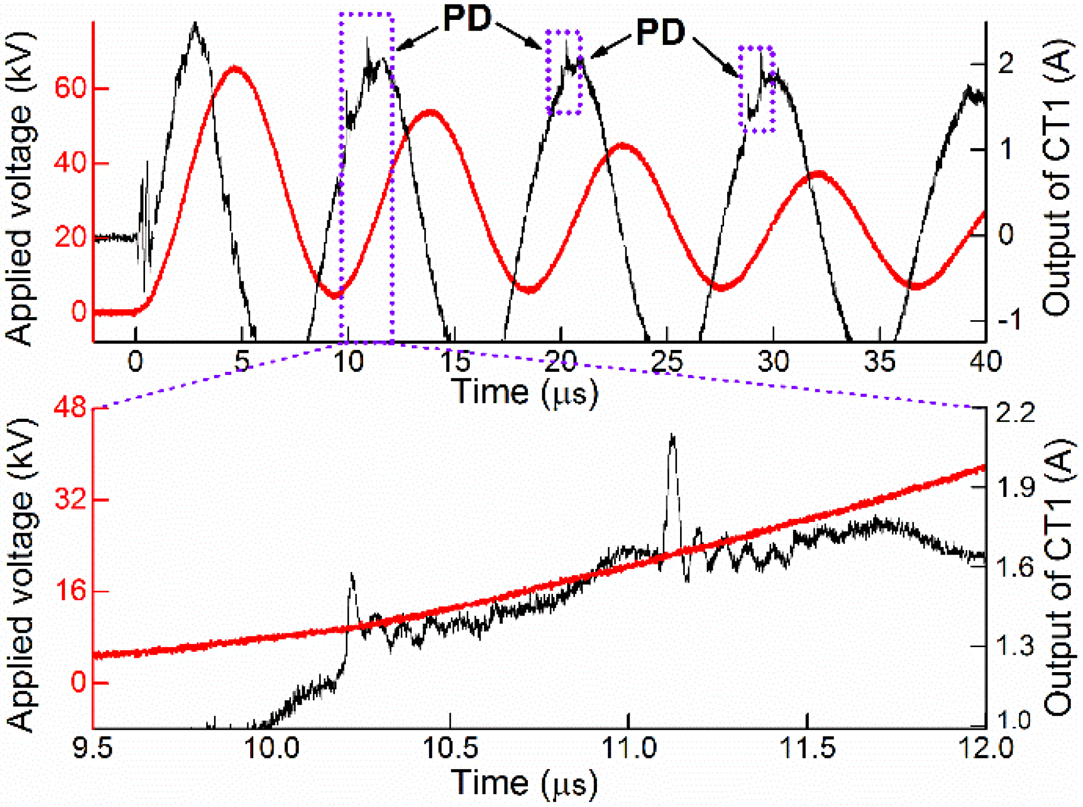
3.1. PDs under OSI Voltage

The differences in the PDs caused by various defects are reflected in their PD sequences in terms of the pulse magnitude and time interval. The various PD sequences involve complicated mechanisms ranging from the generation of an initiatory electron to streamer corona and leaders in the same or different channels, which have been discussed in our previous work [12]. Overall, the three different types of PD sequences occurring in the different interfaces are described in general as follows:
i. PDs at the metal protrusion in the gas: As described in our previous paper [12], the various types of PD sequences could be detected under impulse voltages including a single pulse, a single pulse followed by successive smaller pulses, compact and incompact multiple pulses, and even reverse-polarity pulses. The single pulse (see Figure 8a(i)) and the compact (see Figure 8a(i)) and incompact multiple pulses (Figure 8a(ii)) are the most common types under an OSI voltage.
ii. PDs from the triple junction between the metal, gas, and insulator: The triple-junction region (the interface where the insulator, electrode, and gas are in close proximity) can accelerate the generation of initial electrons via enhanced field emission and electron release by ion impact and surface photon emission. Therefore, in general, a metal particle on an insulator surface could reduce the electrical strength of the dielectric interface between the gas and the solid. As shown in Figure 8b, even if a relatively low impulse voltage is applied (33 kV, see Figure 8b), the PD is large in magnitude at the rising edges of the oscillating periods. These single or multiple pulses have features similar to those occurring at the protrusion in the absence of an insulator surface but are more active.
iii. PDs in the gaseous voids in an insulator: The lower dielectric constant of the gaseous voids results in a locally enhanced field that causes PDs to occur successively inside the void. Under an impulse voltage, the rate of change in the applied electric field with time is greater than the dissipation rate of the PD residual charges in the void. In this case, the direction of the total electric field is changed when the background electric field decreases to a certain value, resulting in reverse-polarity PDs, most of which consist of successive pulses with a high repetition rate. The typical PD sequences detected for a void in an insulator under an OSI are shown in Figure 8c.

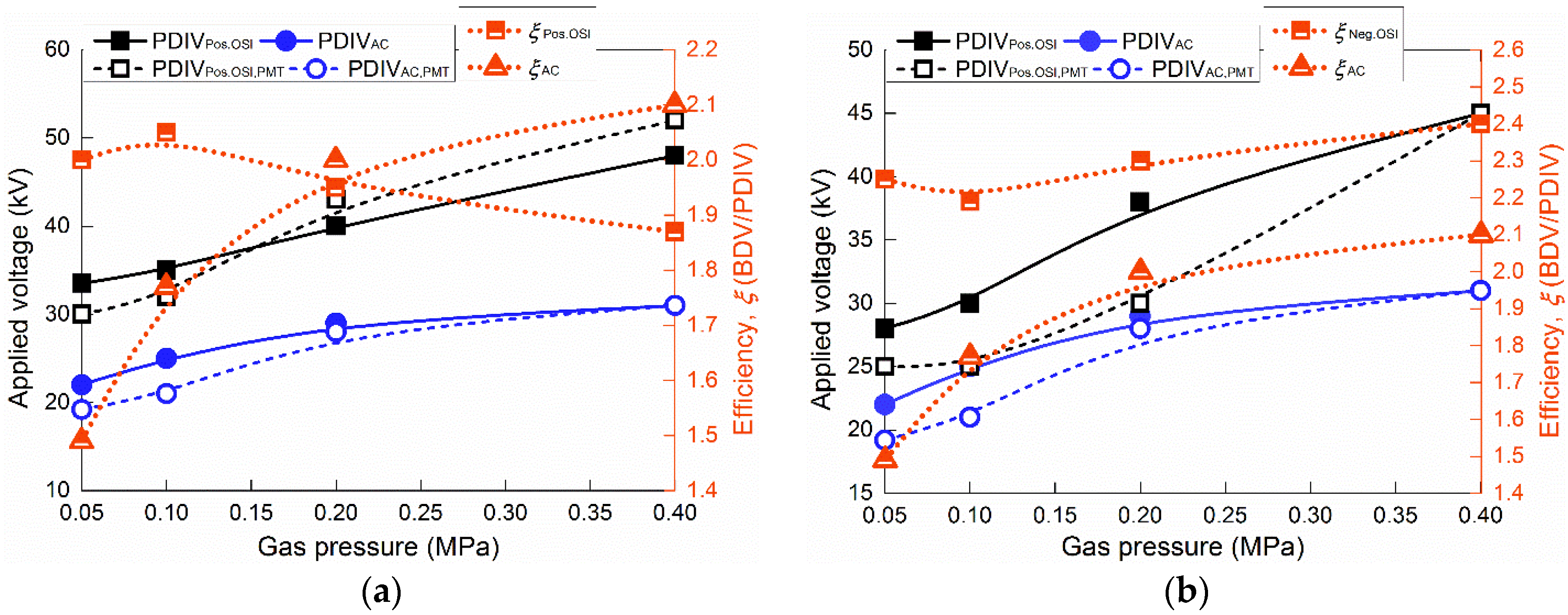
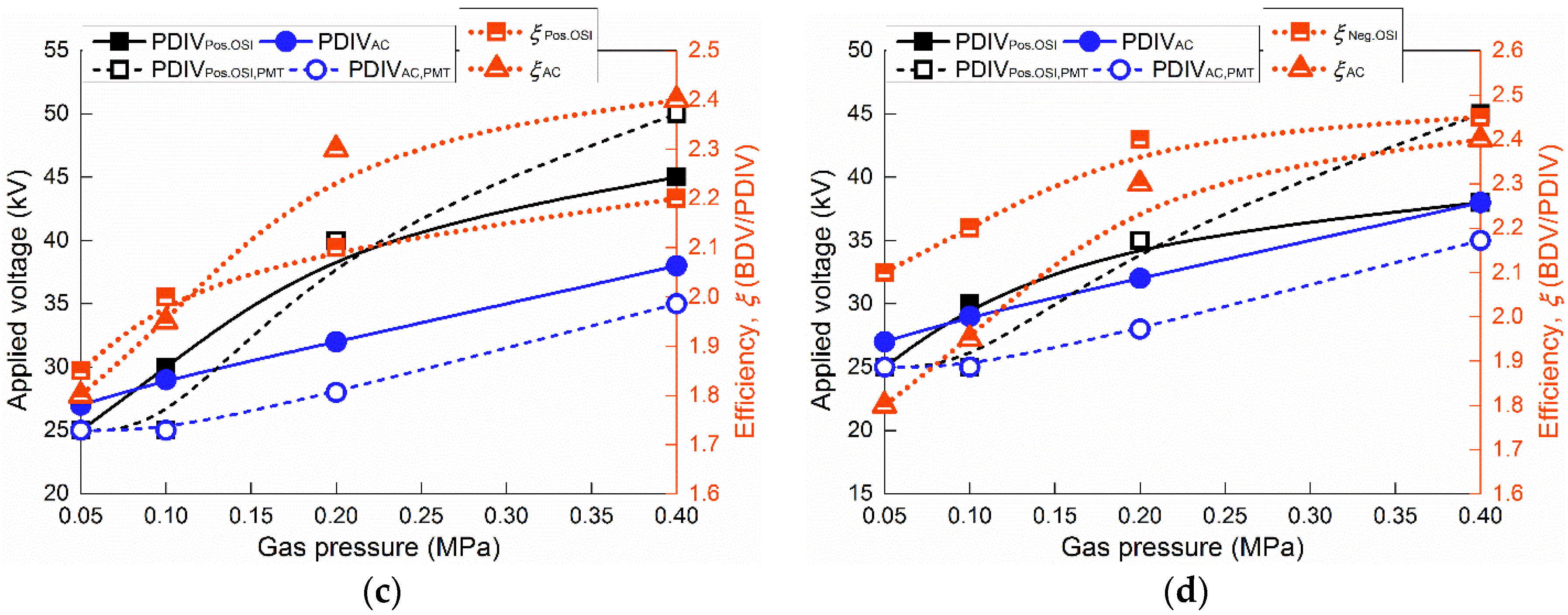
3.2. Efficiencies of the OSI, SI, and AC Voltages for Exciting PDs

3.2.1. PD Inception and Breakdown under Various Applied Voltages

Potential insulation defects are expected to be eliminated by manufacturing and a field test before the power equipment is put into operation. Owing to corona stabilization, some potential defects are not sensitive to the power frequency AC. With an increase in the applied voltage, the insulation will experience the process from PD inception to complete flashover, which makes PD detection possible. For manufacturers and power operation departments, they hope the defects can be detected at a relatively low applied voltage below breakdown voltage. Therefore, a sufficient difference between the inception voltage and the breakdown voltage (BDV) is the premise of an effective PD diagnosis. For example, to find the detectable PDs under applied voltage of 0.7 times BDV is certainly better than under 0.9 times BDV. However, discharges excited by defects are driven by complex mechanisms in different ways. The time lag of the initiatory electron, the probability of avalanche formation, and the effect of space charge stabilization are involved. Although some studies and the reports of International Council on Large Electric Systems (CIGRE) workgroups [15,16,17] have summarized the availabilities of different types of voltages for examining the insulation status, the effectiveness of these voltages has not been quantitatively investigated through experiments.
To quantify the effectiveness of the AC, SI, and OSI voltages for exciting PDs, the detectable scale of the defects was also investigated under various applied voltages. Then, the PD inception voltage (PDIV) and the PD excitation efficiency ξ, which is defined as the ratio of the BDV to the PDIV (Equation (1)), were analyzed for different cases. For a specific applied voltage type, greater efficiency ξ means a lower applied voltage under which the detectable PDs can be exited from a defect. By this parameter, the capabilities of the different applied voltage on exciting detectable PDs can be evaluated and compared quantitatively.
ξ = BDV 50 % PDIV 50 %
where BDV50% is breakdown voltage at fifty percent probability and PDIV50% is partial discharge inception voltage at fifty percent probability.
Figure 9 shows the PDIVs and the values of ξ for different defects under AC and positive OSI voltages as a function of the gas pressure. For the two types of defects exposed to a SF6 gas atmosphere, their PDIVs increased as the gas pressure increased in the range of 0.05–0.4 MPa. As predicted, for a protrusion, the PDIVs of both the positive and negative points under an OSI voltage are greater than those under an AC voltage over the entire range of gas pressures investigated. This is attributed to the presence of the time lag prior to the first discharge. For a particle on an insulator, the PDIVs under an OSI voltage are greater than those under an AC voltage, except for a low gas pressure. The PD excitation efficiency for a negative OSI voltage is greater than that of an AC voltage for gas pressures less than 0.2 MPa but lower for gas pressures greater than 0.2 MPa. For most cases investigated, the efficiency of the positive OSI voltage is greater than that of the AC voltage. In general, the OSI voltage provides PD detection with a more sufficient margin below the BDV compared to the AC voltage, especially for extreme locally enhanced defects such as a protrusion and a particle on an insulator surface. Moreover, in most cases, ξ exhibits an increasing trend as the gas pressure increases. It is inferred that this upward trend in ξ is attributed to the intensifying corona stabilization, which is an intrinsic feature of SF6 in the gas pressure range from one to several bars.

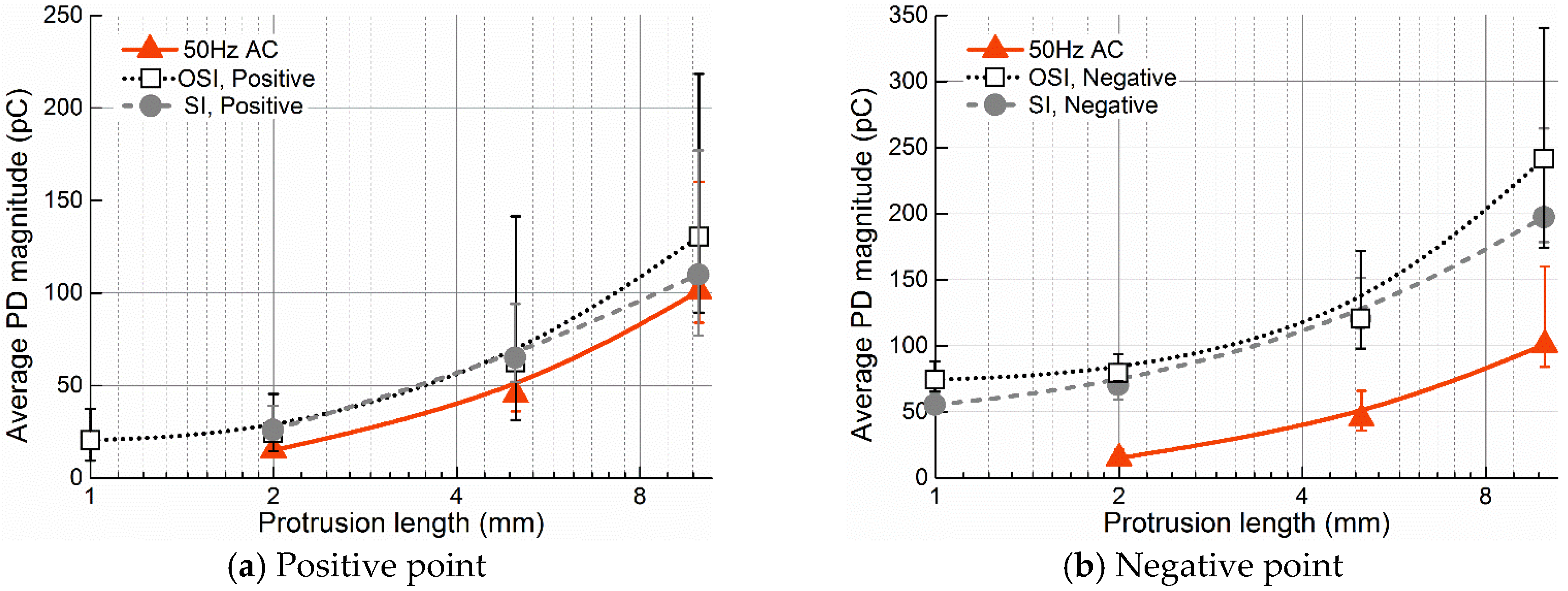
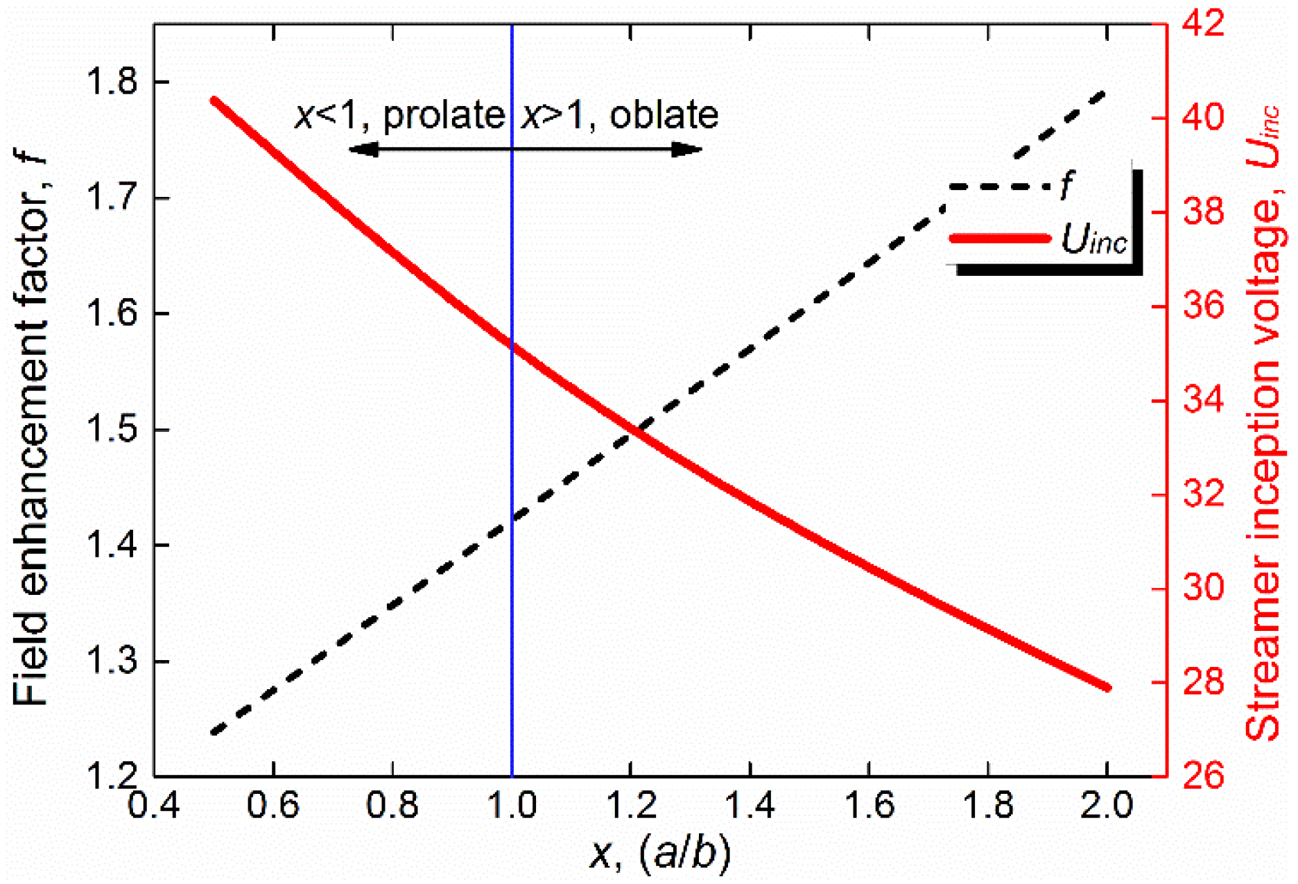
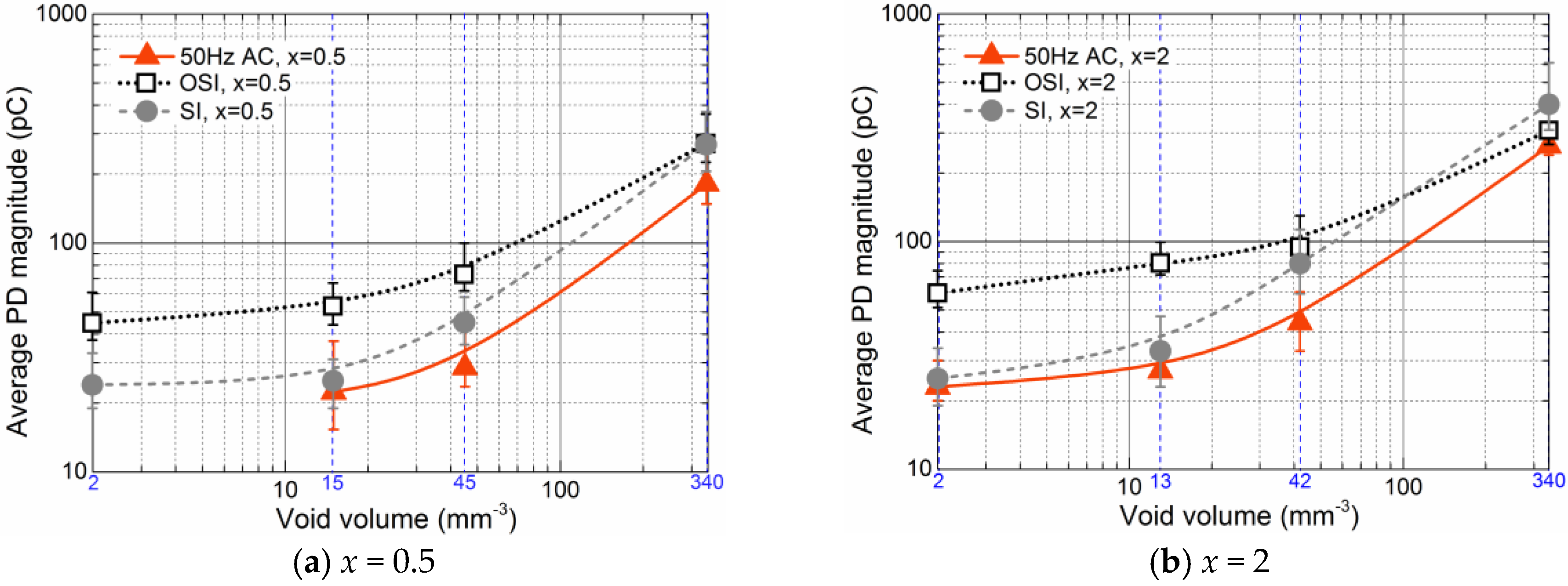
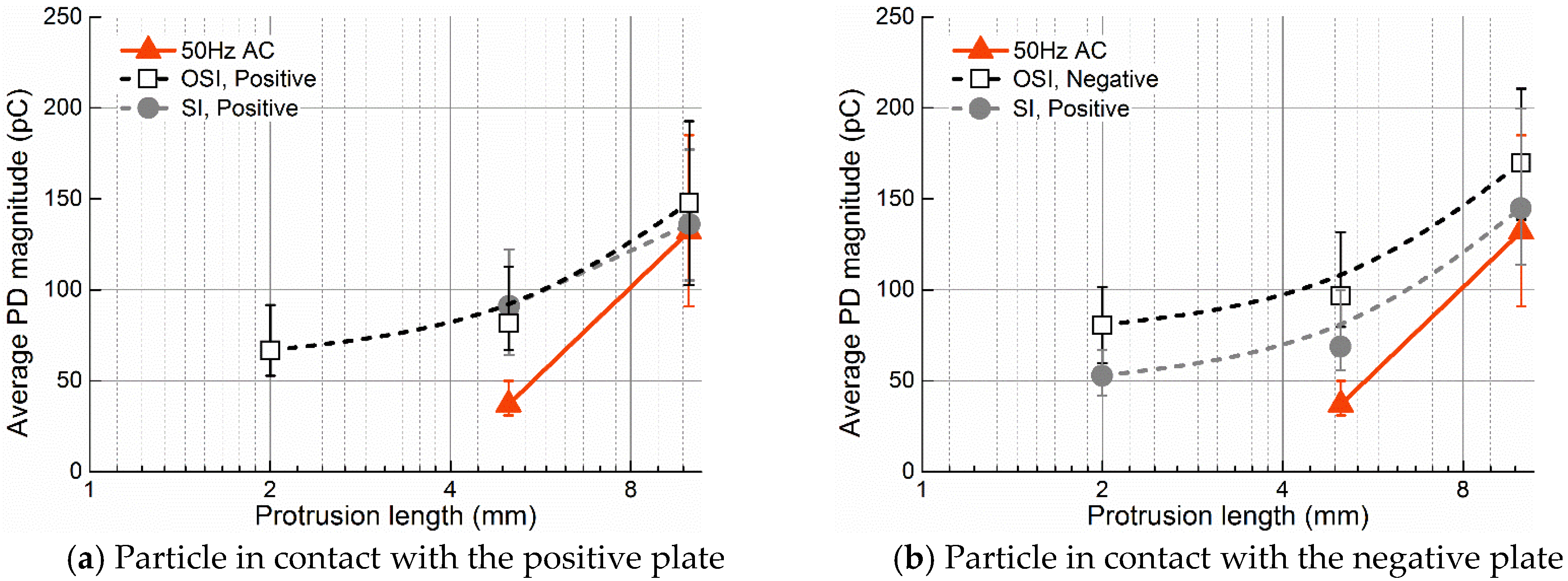
3.2.2. Detectable Scales of the Three Defects under Various Applied Voltages

Electrical discharges in an insulation system could be characterized by the order of magnitude, the detectability, and the relevance for aging and failure. The different types of discharges could be classified as noncritical and critical for insulation. Some noncritical discharges such as surface emission, glows, and Townsend avalanches that exist during normal operation are characterized by very low and quasi continuous currents. Critical discharges such as streamers, leaders, and sparks are caused by a defect-induced locally enhanced electric field and relevant to the aging and failure of dielectric insulation. Although most types of discharges have a pulsed nature, not all of them can be detected by the sensitivity limited PD measurement owing to the low intensities. Therefore, a streamer type discharge is of great concern in PD diagnosis because it induces a detectable pulsed current and is the root of more intensity types such as leaders, sparks, and breakdown. The intensity and the probability of the occurrence of this type of discharge depend upon the electric field for excitation and the geometry and scale of the defect. The minimum detectable scales of the three types of defects under SI, OSI, and AC voltages were investigated experimentally and are quantitatively summarized in this section.
For a void in an insulator, the critical field of the streamer discharge inception voltage is determined by its volume and shape. The shape of the void can be described by the ratio of the radius (a) to the length (b) (denoted by x). According to Pederson’s Model [18], the critical corona inception voltage, Uinc, can be estimated by
U inc = ( E / p ) cr p d F
where the function F depends on the product of gas pressure (p) and defect radius (r) for a void and is given by
F = [ 1 + B / ( 2 p r ) n ] f 1
where B = (Kcr/C)1/β·(E/p)cr−1 and f = 3εr/(2εr + 1). For an air-filled void, Kcr = 9, C = 4.15 × 10⁻⁴, n = 1/β, β = 2, and (E/p)cr = 25 V·(Pa·m)−1. f is the dimensionless field enhancement factor defined in Equation (4). In this work, f was determined by a finite element method (FEM).
Δ U void = f E 0 l
where ΔUvoid is the potential difference along the void; E0 is the background electric field; l is the length of the defect, i.e., 2b.
To investigate the influence of void shape on electric field distribution, FEM numerical calculations were performed on the voids in dielectric with different ratio x but the same volume. It indicates that, the dimensionless field enhancement factor (f) defined in Equation (4) decreases approximately linearly with the increase of x. Based on Equation (3) and Equation (4), the critical corona inception voltage (Uinc) is indicated to increase with the increase of the ratio (x). Figure 10 shows the field enhancement factor of the void and the streamer inception voltage versus x (the ratio of the radius (a) to the length (b)). It can be concluded that the prolate void in the insulator is more critical than the oblate void, even though they have the same volume because the former can induce a greater Laplace field. It is noted that this inception voltage can be thought of as a necessary but not sufficient condition for PD occurrence because the time lag for the initiatory electron should also be considered. In this study, two groups of void defect models with x = 0.5 and 2 are employed to investigate the PD intensity under different applied voltages.
Gaseous voids were created at the center of the gap length between the upper and lower plate electrodes to ensure a symmetrical field distribution. The polarity effect could not be exerted on the PD events. Thus, a conclusion can be drawn by applying one polarity impulse to the sample. The average PD magnitudes as a function of the void volume with prolate (x = 0.5) and oblate (x = 2) shapes are shown in Figure 11a,b, respectively. Compared with the prolate voids, the oblate voids produced PDs with a higher intensity, which were reflected in the pulse magnitudes (pC). The AC voltage was not able to excite PDs above the detectable level (5 pC) for a small prolate void with a volume of 1.5 mm3. In contrast, the PD under an OSI voltage has the greater average magnitude, even for a void with a volume of 1.5 mm3; it is greater than 30 pC. The magnitudes of the PDs under an SI voltage were between those under AC and OSI voltages for most cases, except for the oblate void with a volume of 340 mm3, of which the PD magnitude is greater than that of the OSI voltage. In general, the PD intensity shows an obvious increase by two orders of magnitude as the void volume increases from 1.5 to 340 mm3.
It is noted that a tiny void in an actual insulator is not analogous to the electrode spacing in real equipment. The signal induced in the coupling circuit is immeasurably low and thus obscured by noise. In reality, a detectable void in real scale equipment is larger than expected.
With respect to the protrusion defect in a uniform field, its corona inception and PD charge are sensitive to the protrusion length [19]. With this consideration, the influence of the protrusion scale on the PD behaviors is investigated by changing the length of the protrusion fixed to one of the parallel plates from 1 to 10 mm. The radius of the protrusion was 1.4 mm, and this value merely affects the time lag for PD inception and has a limited effect on PD propagation. Thus, the shape of the protrusion tip does not have an effect on the PD charge.
Figure 12 shows the average PD magnitudes as a function of the protrusion length under OSI, SI, and AC voltages. As expected, more intense PDs occur for longer protrusions stressed by either positive or negative impulses. An obvious polarity effect is observed when comparing the results under positive and negative impulse voltages. The PD magnitudes under positive OSI and SI voltages are similar and slightly greater than those under an AC voltage (see Figure 12a). The significant differences between the PD magnitudes under impulses and an AC voltage could be found at the negative point of the protrusion, as shown in Figure 12b. Moreover, the OSI voltage has a better performance regarding the excitation of PDs with detectable magnitudes from small protrusions.
In general, in the presence of a metal particle on an insulator surface, PDs are initiated from the triple junction of the gas, insulator, and particle where the local field is enhanced and the initiatory electrons emerge. The PD activity is partly related to the field distribution on the insulator surface. In this study, metal needles with different lengths were employed as the particle and were fixed on the insulator surface in contact with the plate electrode. Figure 13 shows the dependence of the average PD magnitude on the protrusion length. As with the protrusion, the polarity effect was also observed for the particle on the insulator surface. The PD magnitudes for various protrusion lengths under an OSI voltage were much greater than those under SI and AC voltages. In the test, all of the types of voltages investigated were incapable of exposing protrusions with a length less than 2 mm, which is still a hazardous in an actual situation.

4. Discussion

Once the discharges occur, the initial Laplace electric field is distorted by the residual charges and is subject to a Poisson distribution. The charge caused by discharges can accumulate in space, resulting in a charge cloud that may reduce the electric field in the vicinity of the protrusion tip. In some cases, this stabilization effect can retard the development of a discharge below a detectable level; thus, an increased background electric field is needed to initiate high-intensity discharges such as a streamer or leader. In the case of an impulse voltage stress, the growth rate of the field can be greater than the mobility of the space charge; thus, the stabilization effect can be limited. This can be used to explain why the PD magnitude under impulse voltages is greater than that under AC or other stable voltages.
The interaction between the electric field and the discharge is simply diagrammed in Figure 14. Vcr is defined as the boundary region where the background electric field Eb exceeds the critical value Ecr for effective ionization (for SF6, (E/p)cr·p = 88.5 kV/cm); vc is defined as the boundary of the space charge diffusion region. The dissipation time of the charge in the gas zone (tsw) depends on the electric field distribution in front of the discharge channel [10]. If the applied background electric field slowly increases, the charge diffusion region vc moves in front of the critical field region Vcr, and the propagation of the discharge stops before it extends to the critical length for streamer (lcr). On the contrary, if the applied background electric field rapidly increases, vc < Vcr, and an intensive discharge can develop. For a void in an insulator, the first PD is initiated without residual charge in the void when Eb is sufficiently high (Eb > Estr), and an initiatory electron is generated. After that, a reverse field (Er) is developed inside the void and limits the total field strength. The subsequent PDs start once the total field strength (EbEr) is recovered above a critical level by increasing the background field.

5. Conclusions

PD detection under impulse voltage conditions, has been investigated based on three artificial test models in terms of the measurement method, test object, and PD behavior. The general PD sequence features were briefly summarized by exemplifying the typical PD pulses of different defects under an OSI voltage. The single pulse, multiple pulses, and the reverse polarity pulse with different mechanisms were considered to be the main components of the PD sequences. Although the PDIVs under an OSI voltage were greater than those under an AC voltage over entire range of gas pressures investigated, the PD excitation efficiency, i.e., the ratio of the BDV to the PDIV, under an OSI voltage is greater than that under an AC voltage for most cases, which means PD detection under an OSI voltage has a more sufficient margin below the BDV. It was also found that the OSI voltage has good performance for the excitation of PDs from a small-scale defect with more detectable magnitudes. In contrast, an AC voltage is incapable of finding some defects even with hazardous scales. The good detectability imparted by the impulse voltages accounts for the weakened corona stabilization under an impulse. The authors believe that, in the case of an impulse voltage stress, the growth rate of the field can be greater than the mobility of the space charge; thus, the stabilization effect can be limited.

Acknowledgments

The authors would like to thank the National Natural Science Foundation of China (Grant No. 51507130), China Postdoctoral Science Foundation (Grant No. 2014M560777), Special China Postdoctoral Science Foundation (Grant No. 2016-11-141158), Shaanxi International Cooperation and Exchanges Foundation (Grant No. 2016KW-072) and Fundamental Research Funds for the Central Universities.

Author Contributions

M.R. and M.D. conceived and designed the experiments; C.Z. and J.Z. performed the experiments and relevant simulations; M.R. and C.Z. analyzed the data; M.R. wrote the paper.

Conflicts of Interest

The authors declare no conflict of interest.

References

  1. CIGRE Joint Task Force. Partial Discharge Detection System for GIS: Sensitivity Verification for the UHF Method and the Acoustic Method. Electra 1999, 183, 75–87. [Google Scholar]
  2. Takahashi, T.; Yamada, T.; Hayakawa, N.; Okubo, H. Space charge behavior in SF6 gas and sequential generation of PD pulses. IEEE Trans. Dielectr. Electr. Insul. 2000, 7, 141–145. [Google Scholar] [CrossRef]
  3. Hinterholzer, T.; Boeck, W. Breakdown in SF6 influenced by corona-stabilization. Electr. Insul. Dielectr. Phenom. 2000, 1, 413–416. [Google Scholar]
  4. High-Voltage Test Techniques-Part 3: Definitions and Requirements for On-site Testing; International Electrotechnical Commission (IEC): Geneva, Switzerland, 2006.
  5. Meijer, S.; Gulski, E.; Smit, J.J.; Kanters, A.J.L. Risk assessment of fixed defects in GIS under different voltage wave shapes. In Proceedings of 18th International Conference and Exhibition on Electricity Distribution, Turin, Italy, 6–9 June 2005.
  6. Okabe, S.; Yuasa, S.; Kaneko, S.; Ueta, G. Evaluation of breakdown characteristics of gas insulated switchgears for non-standard lightning impulse waveforms method-method for converting non-standard lightning impulses waveforms into standard impulse waveforms. IEEE Trans. Dielectr. Electr. Insul. 2009, 16, 42–51. [Google Scholar] [CrossRef]
  7. Anis, H.; Srivastava, K.D. Breakdown of rod-plane gaps in SF6 under positive switching impulses. IEEE Trans. Power App. Syst. 1982, 101, 537–546. [Google Scholar] [CrossRef]
  8. Niemeyer, L.; Ullrich, L.; Wiegart, N. The mechanism of leader breakdown in electronegative gases. IEEE Trans. Electr. Insul. 1989, 24, 309–324. [Google Scholar] [CrossRef]
  9. Hayakawa, N.; Yoshitake, Y.; Koshino, N.; Ueda, T.; Okubo, H. Impulse partial discharge characteristics and their mechanisms under non-uniform electric field in N2/SF6 gas mixture. IEEE Trans. Dielectr. Electr. Insul. 2005, 12, 1035–1042. [Google Scholar] [CrossRef]
  10. Wiegart, N.; Niemeyer, L.; Pinnekamp, F.; Boeck, W.; Kindersberger, J.; Morrow, R.; Zaengl, W.; Zwicky, M.; Gallimberti, I.; Boggs, S.A. Inhomogeneous field breakdown in GIS-the prediction of breakdown probabilities and voltages. III. Discharge development in SF6 and computer model of breakdown. IEEE Trans. Power Deliv. 1988, 3, 939–946. [Google Scholar] [CrossRef]
  11. Niemeyer, L. A generalized approach to partial discharge in modeling. IEEE Trans. Dielectr. Electr. Insul. 1995, 2, 510–528. [Google Scholar] [CrossRef]
  12. Ren, M.; Dong, M.; Xiao, Z.; Qiu, A. Partial discharge pulses at artificial protrusions in SF6 under negative IEC 60060-3 standard impulses. IEEE Trans. Dielectr. Electr. Insul. 2014, 21, 273–283. [Google Scholar] [CrossRef]
  13. Ren, M.; Dong, M.; Xiao, Z.; Qiu, A. Partial discharges in SF6 filled void under standard aperidic and oscillating switching impulses. IEEE Trans. Dielectr. Electr. Insul. 2014, 21, 262–272. [Google Scholar] [CrossRef]
  14. Densley, R.J.; Salvage, B. Partial Discharges in Gaseous Cavities in Solid Dielectrics under Impulse Voltage Conditions. IEEE Trans. Electr. Insul. 1971, EI-6, 54–62. [Google Scholar] [CrossRef]
  15. CIGRE Working Group. Insulation coordination of GIS: Return of experience, on site tests and diagnostic techniques. Electra 1998, 176, 67–95. [Google Scholar]
  16. Haller, R.; Hauschild, W.; Mosch, W. High-voltage field testing of GIS from a physical view-point. In Proceedings of the Second International Conference on Properties and Applications of Properties and Applications of Dielectric Materials, Beijing, China, 12–16 September 1988.
  17. Kornhuber, S.; Boltze, M.; Haller, R.; Mraz, P.; Pihera, J. PD behavior of basic test arrangements under different measurement conditions. In Proceedings of the International Conference on Condition Monitoring and Diagnosis (CMD), Bali, Indonesia, 23–27 September 2012.
  18. Crichton, G.C.; Karlsson, P.W.; Pedersen, A. Partial Discharges in Ellipsoidal and Spheroidal Voids. IEEE Trans. Electr. Insul. 1989, 24, 335–342. [Google Scholar] [CrossRef] [Green Version]
  19. Seeger, M.; Niemeyer, L.; Bujotzek, M. Partial discharges and breakdown at protrusions in uniform background fields in SF6. J. Phys. D: Appl. Phys. 2008, 41, 185204. [Google Scholar] [CrossRef]
Figure 1. On-going oscillating impulse withstand test implemented on gas insulated switchgear in the field.
Energies 09 00623 g001
Figure 2. PD signals superimposed on the current flow under an impulse.
Energies 09 00623 g002
Figure 3. A preposing signal process circuit for PD measurement. The loop consisting of C1, C2, C3, R1, and R2 is employed as a second-order RC filter. R3 and R4 are used for gain control.
Energies 09 00623 g003
Figure 4. Measurement circuits for impulse PD detection. Rs: the current-limiting resistor, 1 MΩ; C0: the test sample, 60–160 pF; Cp: the coupling capacitor for PD detection, 1.6 nF; C1: the DC charging capacitor, 0.0111 µF; Rf: the wave-front-adjusting resistor, 3.0 kΩ; Rt: the wave-tail-adjusting resistor, 300 kΩ; Lf: the adjusting inductor, 85.3 mH.
Energies 09 00623 g004
Figure 5. The waveform of the OSI voltage. T1: front time; T2: time-to-half-value; f: oscillating frequency.
Energies 09 00623 g005
Figure 6. SF6 test chamber and PD defect models. (a) Test chamber with PD sensors; (b) Metal protrusion; (c) Metal particle on insulator surface; (d) Gaseous void in insulator. The plate electrodes are made of copper, and the protrusion and needle are made of steel. D is the gap distance between the plate electrodes. θ is the inclination angle of the insulator. L is the length of the protrusion or the needle on the surface. a and b are the radius and the height of the gaseous void in the insulator, respectively. The permittivity of epoxy is 4.1.
Energies 09 00623 g006
Figure 7. Schematic of the overall impulse PD detection system.
Energies 09 00623 g007
Figure 8. PD current and light pulses (sequences) excited by the three defects in a SF6-insulated system under OSIs. (a) a protrusion fixed on a ground plate, 42 kV OSI, negative high voltage (HV); (b) metal particle on an insulator surface in contact with the HV plate, 38 kV OSI, positive HV; (c) cylindrical void inside an insulator filled with air, 33 kV OSI, positive HV.
Energies 09 00623 g008
Figure 9. Values of the PDIV and the ratio of the BDV to the PDIV for different defects under AC and positive OSI voltages versus the gas pressure for (a), (b) a metal protrusion fixed on a conductor under positive and negative voltages and (c), (d) a metal particle on an insulator surface in contact with the electrode under positive and negative voltages.
Energies 09 00623 g009aEnergies 09 00623 g009b
Figure 10. The influence of the void shape on the electric field in the void and the streamer inception voltage. The volume of the void in the calculation is 1.57 mm3. The relative permittivities of the insulator and the gas in the void are 4.1 and 1.0, respectively. The surface resistivity of the inner face of the void is 10−20 Ω.
Energies 09 00623 g010
Figure 11. Average PD magnitude versus the volume of the void in the insulator. The OSI, SI, and 50 Hz AC voltages applied to the samples are equal to 1.6 times the PDIV.
Energies 09 00623 g011
Figure 12. Average PD magnitude versus the protrusion length. The OSI, SI, and 50 Hz AC voltages applied to the samples are equal to 0.7 times the BDV. The radius of the protrusion is 0.8 mm.
Energies 09 00623 g012
Figure 13. Average PD magnitude versus the length of the needle-like particle on an insulator surface. The OSI, SI, and 50 Hz AC voltages applied to the samples are equal to 1.6 times the PDIV. The diameter of the protrusion is 1.4 mm.
Energies 09 00623 g013
Figure 14. Comparison of PD propagation affected by the space charge under a slowly varying voltage and an impulse voltage.
Energies 09 00623 g014
Table 1. Scale parameters of the three defects investigated.
DefectsGap Between the Plate Electrodes
(Background Field)
Defect Scale Parameters
(Locally Enhanced Field)
ProtrusionD = 30 mmr = 0.7 mm, L = 1, 2, 5 10 mm
Surface particleD = 35 mm, θ = 60°r = 0.7 mm, L = 1, 2, 5, 10 mm
VoidD = 20 mmx{=a/b} = 0.5, 2
V{=πa2b} = 2, 15, 45, 340 mm3

