1. Introduction
In high-performance applications, the high switching frequency is the least requirement for power inverters to achieve high dynamical response and high precision [
1]. However, hard-switching power inverters suffer from large switching loss and severe electromagnetic interference (EMI) as the switching frequency increases [
2,
3].
In order to solve the problems of large switching loss and severe EMI in a power inverter with high switching frequency, the use of the soft-switching technique is one of the best options. It utilizes auxiliary components to limit the
di/
dt or
dv/
dt during the commutation period, and thus reduces the overlap between the voltage and current of semiconductor switches. To date, a variety of soft-switching DC-AC topologies have been proposed [
4,
5,
6,
7,
8,
9,
10,
11,
12,
13,
14,
15,
16,
17,
18,
19,
20,
21,
22]. Among them, the zero-voltage transition (ZVT) pulse-width-modulation (PWM) inverters is a typical soft-switching inverters. An auxiliary circuit connected in parallel with the main power path is employed in ZVT PWM inverters, which only operate for a short interval before and after the commutation period of the main switches. This makes ZVT inverters the closest to the PWM converter counterpart. In addition, ZVT PWM inverters have the advantages of operating with soft switching within a wide load range and low voltage and current stresses over other types of soft-switching inverters.
Several topologies of the ZVT PWM inverters have been proposed. The auxiliary resonant commutated pole inverter (ARCPI) has been proposed with two auxiliary switches per phase [
4,
5]. The ARCPI can meet the demand for high efficiency and low voltage and current stresses. However, the major drawback is the existence of the split capacitors, which cause the problems of capacitor charge balance. The auxiliary resonant snubber inverter (ARSI) has been proposed to eliminate the split capacitors, but the three-phase topology cannot utilize the conventional space-vector-pulse-width modulation (SVPWM) [
6,
7]. Thus, they are more suitable for permanent magnet brushless DC motors instead of all types of motors. The single-phase topology is very attractive with only two auxiliary switches and well fit to the conventional PWM. Meanwhile, the ZVT inverter using coupled magnetics has been proposed to eliminate the split capacitors [
8,
9,
10]. However, these topologies need coupled inductors and a large number of auxiliary switches, which increase the cost and difficulty of the circuit realization. The ZVT PWM converter has been synthesized and summarized in [
11,
12].
Although each topology has its drawbacks, the ZVT inverters are widely adopted due to its high efficiency, low EMI noise, available to utilize PWM and low voltage and current stresses. However, the main problem in high-performance applications is the dead-time effect, which brings about distortion and nonlinear voltage error. Extensive studies have been completed on the elimination [
13,
14] and compensation [
15,
16,
17] of the dead-time effect, but they are focused on hard-switching inverters. With the additional auxiliary circuit, the auxiliary current is a new controllable variable in the ZVT PWM inverters compared with hard-switching inverters. Just as the DC-link soft-switching inverter, the zero-voltage notches can influence the output and increase the nonlinearity [
18]. The auxiliary current can also affect the output voltage and current of ZVT PWM inverters, which makes the dead-time effect quite different from that of hard-switching inverters. Besides, the conventional control of ZVT PWM inverters including the fix-timing control [
19,
20] and variable-timing control [
20,
21,
22] aim to improve the efficiency and leads to voltage distortion in turn.
Motivated by the dead-effect elimination of hard-switching inverters and lack of studies about the impact of auxiliary current on linearity of a ZVT PWM soft-switching inverter, this paper analyzes the dead-time effect of a typical example of ZVT PWM soft-switching inverters—ARSI. A high-precision control by controlling the auxiliary current to eliminate the dead-time effect is proposed. A prototype was developed to verify the effectiveness of the proposed control method.
2. Commutation of the Auxiliary Resonant Snubber Inverter
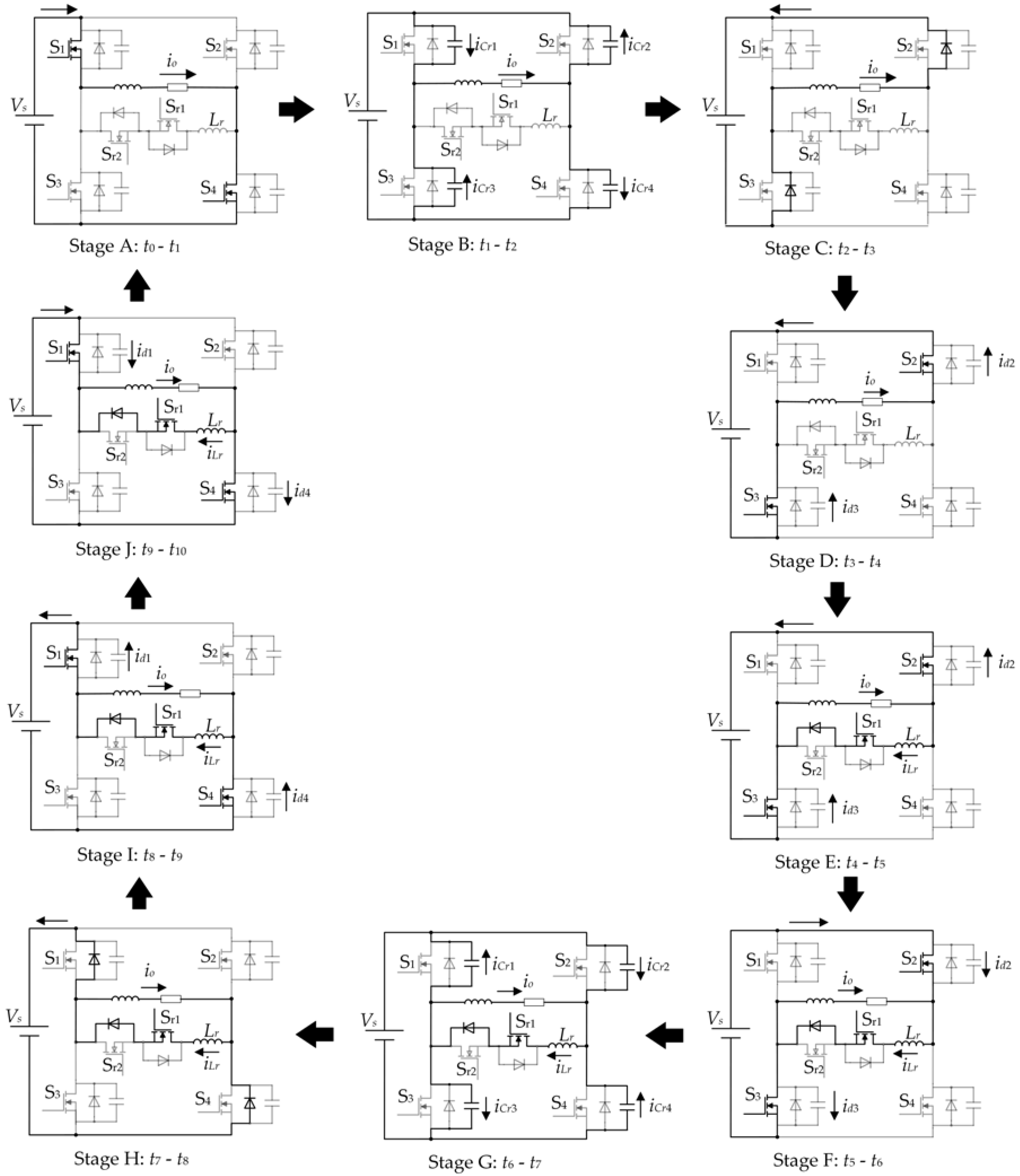
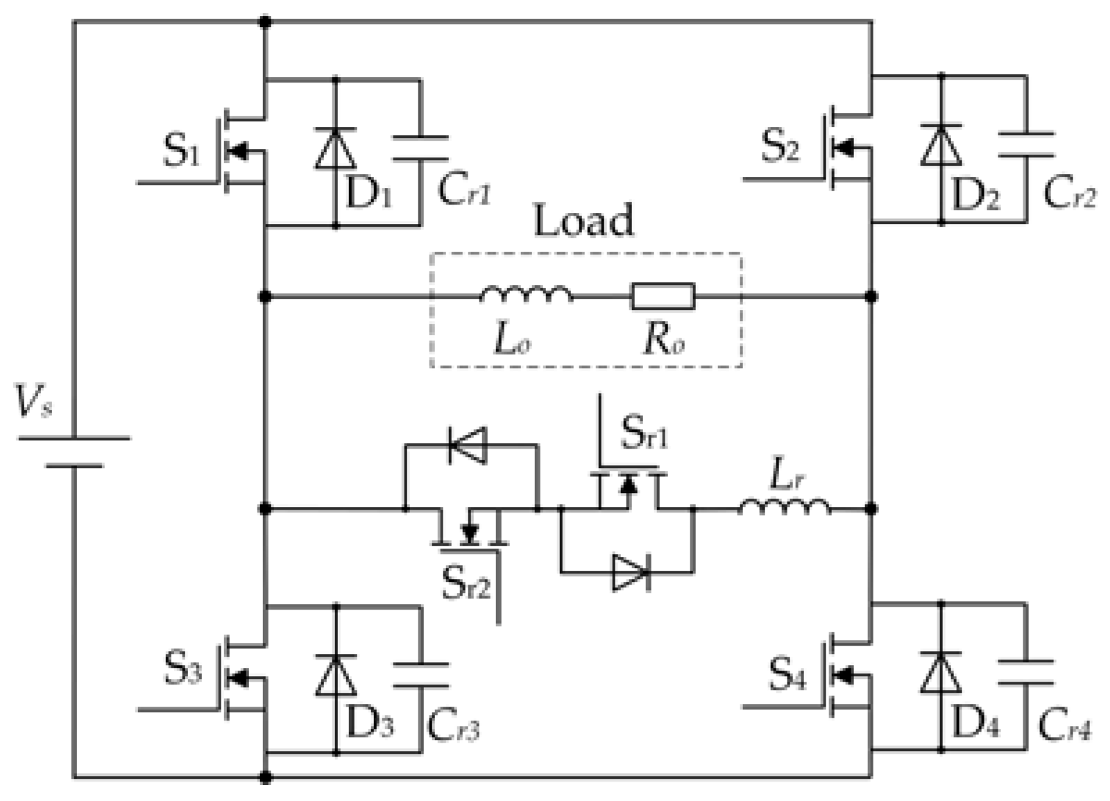
Figure 1 depicts the single-phase ARSI topology analyzed in this paper, which consists of a standard H-bridge inverter, resonant capacitors and an auxiliary circuit. The proper operation of the auxiliary switches S
r1 and S
r2 can create zero-voltage-switching (ZVS) condition for the main switches S
1–S
4. Meanwhile, the auxiliary switches can realize zero-current switching (ZCS).
The detailed circuit operation will be analyzed in the case of positive output current. In the following, we assume that:
- 1)
All components and devices are ideal;
- 2)
The gate signals of the MOSFETs are ideal square-wave;
- 3)
The load Lo is large enough to maintain the load current constant during each switching cycle.
One switching cycle of the operating stages and the operating waveforms are, respectively, shown in
Figure 2 and
Figure 3, where
vds is the drain-source voltage of a MOSFET,
id is the drain current of a MOSFET,
vg is the practical gate signal with dead-time,
vg,id is the ideal gate signal,
iLr is the resonant inductor current,
vab is the practical pole voltage across the load with dead-time,
vab,id is the ideal pole voltage across the load and
verr is the voltage error between
vab and
vab,id.
1) Stage A (
t0–
t1): The main switches S
1 and S
4 fully conducts the load current and S
2 and S
3 are in the off state. Therefore, the pole voltage
vab is expressed as follows:
2) Stage B (
t1–
t2): Due to the existence of the resonant capacitors
Cr1 and
Cr4,
vds1 and
vds4 increase very slowly. Therefore, S
1 and S
4 are turned off at ZVS at
t1. Then, the load begins resonating with four resonant capacitors.
Cr2 and
Cr3 are discharged and
Cr1 and
Cr4 are charged due to the positive load current. The drain-source voltages of MOSFETs can be calculated as follows:
The pole voltage can be obtained as follows:
When
vds2 and
vds3 decrease to zero at
t2, the resonant period is over. The resonant time is calculated as follows:
3) Stage C and D (
t2–
t4): After the
vds2 and
vds3 decrease to zero, the current freewheels through the body diodes D
2 and D
3 and
vds2 and
vds3 are clamped to zero. Therefore, S
2 and S
3 are turned on at ZVS condition at
t3. After
t3, the current is diverted from D
2 and D
3 to the channels of S
2 and S
3. During these stages, the pole voltage
vab can be written as follows:
4) Stage E and F (
t4–
t6): S
r1 is turned on at
t4 at ZCS condition, resulting in charging the resonant inductor with voltage
Vs. The resonant inductor current can be calculated as follows:
At
t5, the resonant inductor current
iLr equals the load current
io. After
t5, S
2 and S
3 work from third quadrant to first quadrant because
iLr is larger than
io. To obtain the resonant inductor current
ILrm, the charging time can be obtained according to Equation (7).
During this stage, the pole voltage is as follows:
5) Stage G (
t6–
t7): The resonant inductor is charged to
ILrm at
t6. Meanwhile, S
2 and S
3 are turned off at ZVS condition at
t6. Thus, the resonant inductor begins resonating with four resonant capacitors.
Cr1 and
Cr4 are discharged and
Cr2 and
Cr3 are charged. The equations during this resonant period can be written as follows.
Therefore, the inductor current and drain-source voltages of the main MOSFETs can be obtained as follows according to Equations (10)–(14).
where
,
, and
ILrm is the initial resonant inductor current.
The pole voltage can be obtained as follows:
For
vds1(
t) = 0, the resonant time can be calculated as:
At the end of the resonant time
t7,
iLr can be obtained from Equations (15) and (19).
6) Stage H–J (
t7–
t10): After the voltages
vds1 and
vds4 decrease to zero, the body diodes D
1 and D
4 conduct the current so that
vds1 and
vds4 are clamped to zero. Therefore, S
1 and S
4 are turned on at the ZVS condition at
t8 and take over the load current. During these stages, the pole voltage can be obtained.
Owing to the positive pole voltage, the resonant inductor is discharged. During the discharging period,
iLr can be calculated as follows:
After the current
iLr decreases to zero, S
r1 are turned off at ZCS condition. The discharging time can be obtained as follows according to Equation (22).
3. Dead-Time Effect and Voltage Error
The duty ratio and output voltage are respectively the direct input and output of the inverters. Thus, the linearity of inverters is related the relationship duty ratio and output voltage.
From the analysis in
Section 2, the pole voltage can be obtained in one switching cycle (
t0–
t10) as follows according to Equations (1), (4), (6), (9), (18) and (21).
The voltage error
verr between the practical pole voltage and the ideal pole voltage can be obtained as follows:
The average voltage error in a switching cycle can be obtained as follows:
The average output voltage can be calculated as follows:
The output voltage is related to not only the duty ratio but also the commutation times according to Equation (27). The nonlinearity of the ARSI is caused by the dead-time effect.
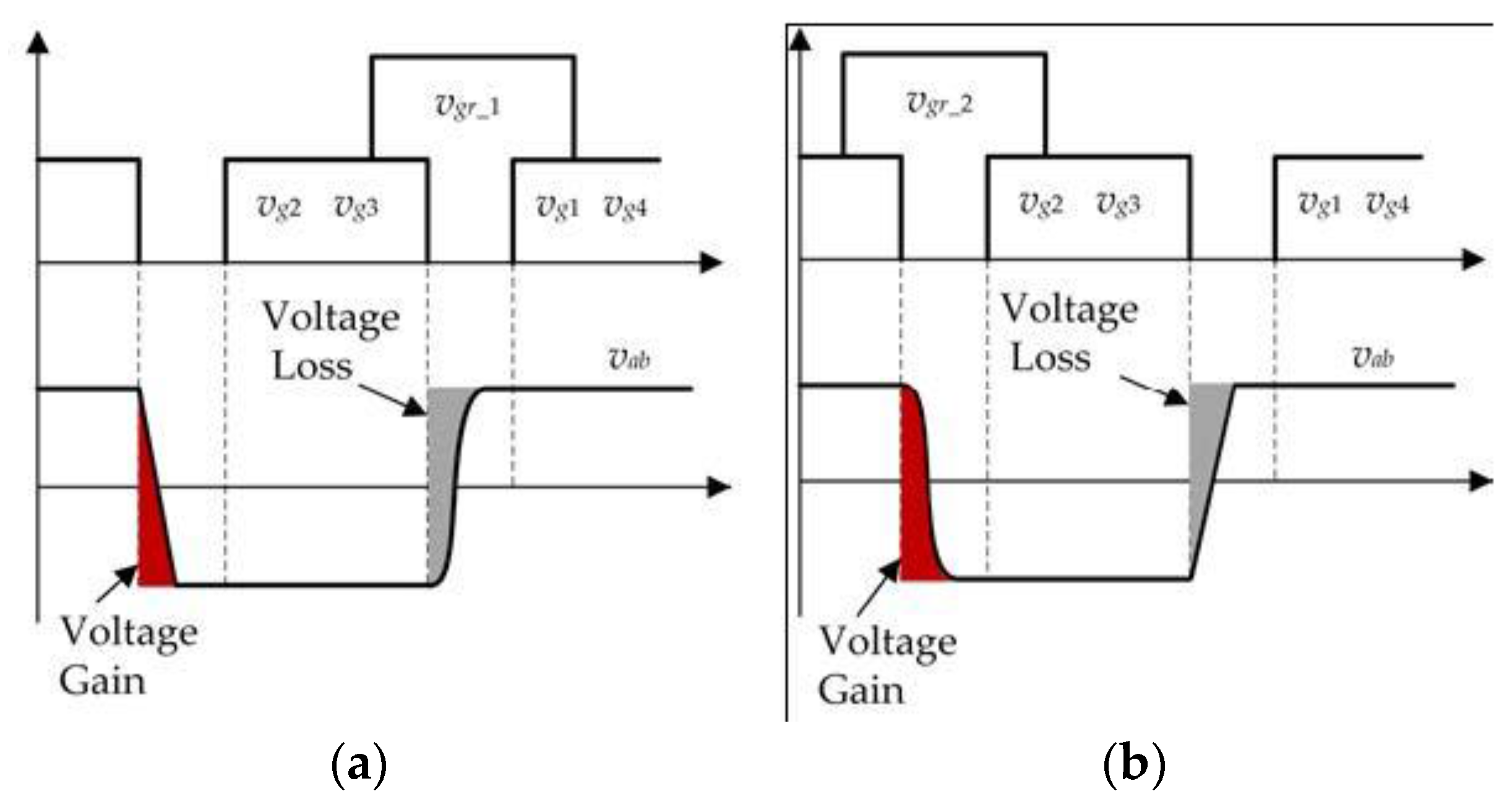
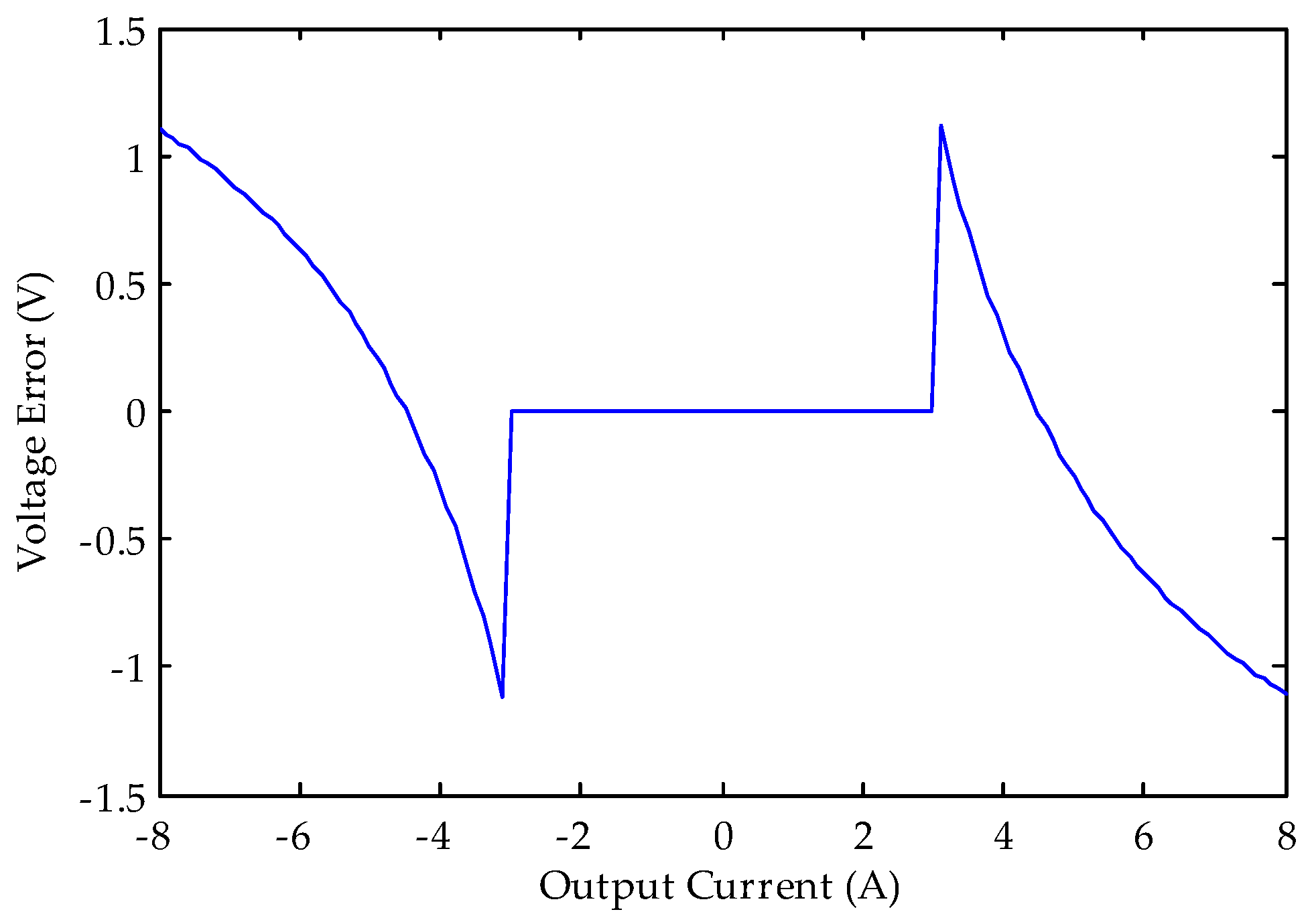
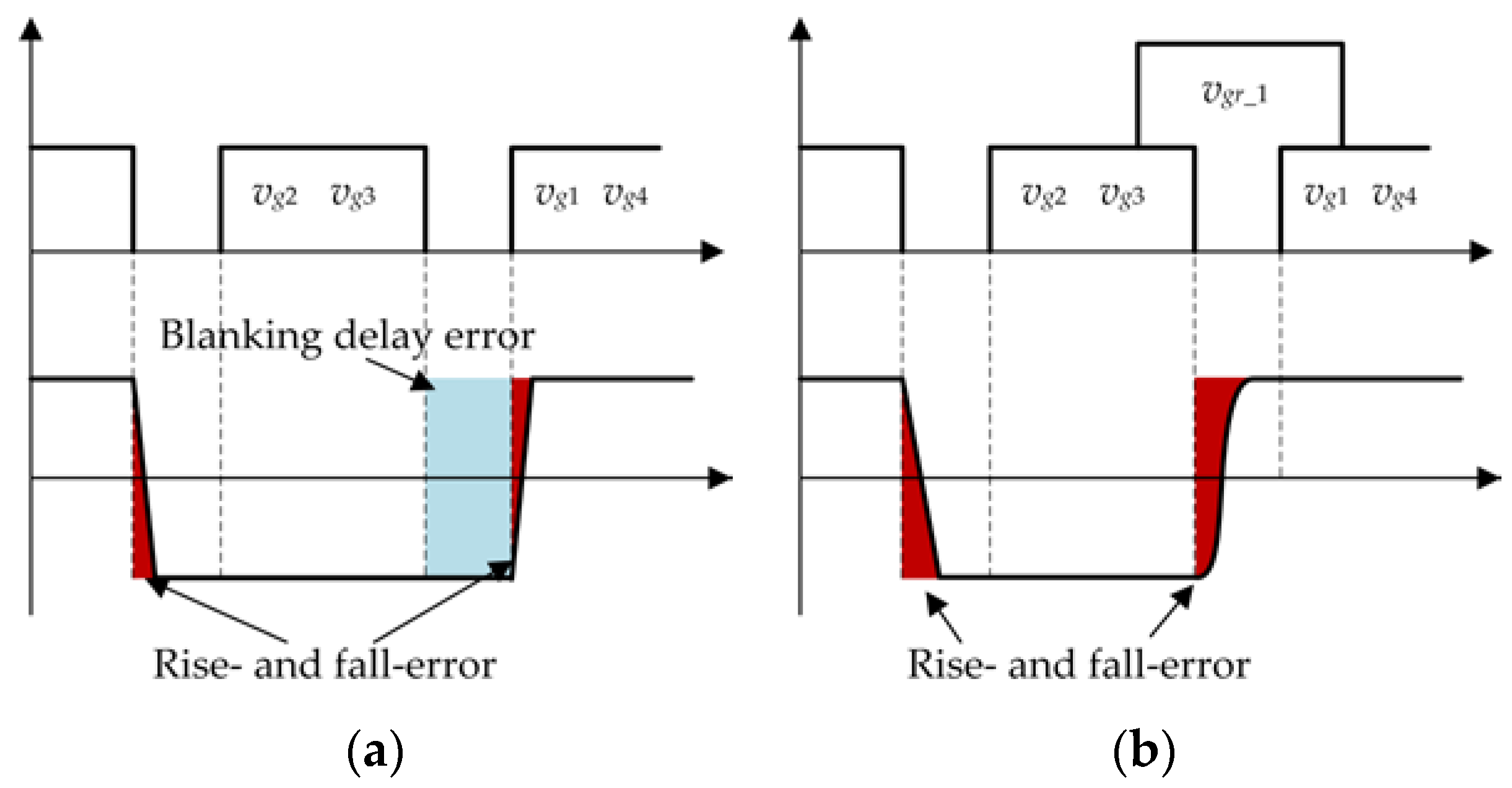
Figure 4 shows when the output current is positive, the dead-time effect of the hard-switching inverter and the ARSI without considering the turn-on and turn-off delay. Due to the finite rise- and fall-times of voltage caused by the output capacitors of MOSFETs, the rise- and fall-errors occur in the hard-switching inverter. Additionally, the dead-time effect also causes the blanking delay error which is the main error source in the hard-switching inverter [
16]. As for the ARSI, only the commutation stages (
t1–
t2) and (
t6–
t7) lead to the voltage errors according to Equation (25). Although the rise- and fall-errors are enlarged in the ARSI due to the additional resonant capacitors compared with the hard-switching inverter, the blanking delay error that caused by the blanking delay times (
t2–
t3) and (
t6–
t7) is eliminated, because the body diodes of the next turn-on MOSFETs conduct the current during the blanking delay time. Therefore, the dead-time effect is reduced in the ARSI.
In one switching cycle, there are two commutations among the main switches. The PTN (positive to negative) commutation is the commutation that the current is diverted from positive switches (S
1 and S
4) to negative switches (S
2 and S
3), while the NTP (negative to positive) commutation is the commutation that the current is diverted from negative switches (S
2 and S
3) to positive switches. In
Figure 3, (
t1–
t2) is PTN commutation and (
t6–
t7) is NTP commutation.
According to Equation (25), the average voltage error of each commutation in a switching cycle can be obtained as follows:
where
trf,PTN is the commutation time of PTN commutation and
trf,NTP is the commutation time of NTP commutation.
When the output current is positive, the S
2 and S
3 realize natural ZVS (NZVS) without the operation of auxiliary circuit during the PTN commutation, while S
1 and S
4 realize auxiliary ZVS (NZVS) with the proper operation of auxiliary circuit during the NTP commutation. According to Equations (28) and (29), the PTN commutation introduce positive voltage error and the NTP commutation create negative voltage error in conclusion. The magnitude of the voltage error is proportional to the commutation time
trf regardless of whether the main switches realize NZVS or AZVS.
Table 1 shows the average voltage errors of the PTN and NTP commutations. The analysis above is discussed in the case of positive output current, but the conclusion can also be used in the condition of negative output current.
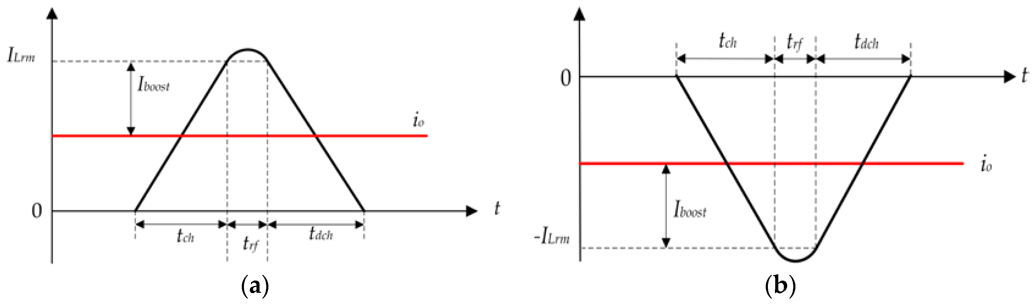
The commutation time
trf is related to the realization of the ZVS type. If the main switches achieve NZVS, the commutation time can be obtained according to Equation (5).
To achieve AZVS with the proper operation of the auxiliary circuit, the commutation time can be obtained according to Equation (19).
where
Iboost is the initial resonant current which is the current to charge and discharge the resonant capacitors
Iboost =
ILrm −
io and
ILrm is the auxiliary current at the beginning of the resonant time.
According to Equations (30) and (31), the commutation time can be summarized in
Table 2. To achieve NZVS, the commutation time is related to the load current. To achieve AZVS, the commutation time is related to the initial resonant current
Iboost.
In a switching cycle, one commutation aims to realize NZVS of the main switches, while the other commutation aims to achieve AZVS. When the output current is positive, NZVS of the main switches can be achieved during the PTN commutation. When output current is negative, NZVS can only be achieved during the NTP commutation. The voltage error can be obtained according to
Table 1 and
Table 2.
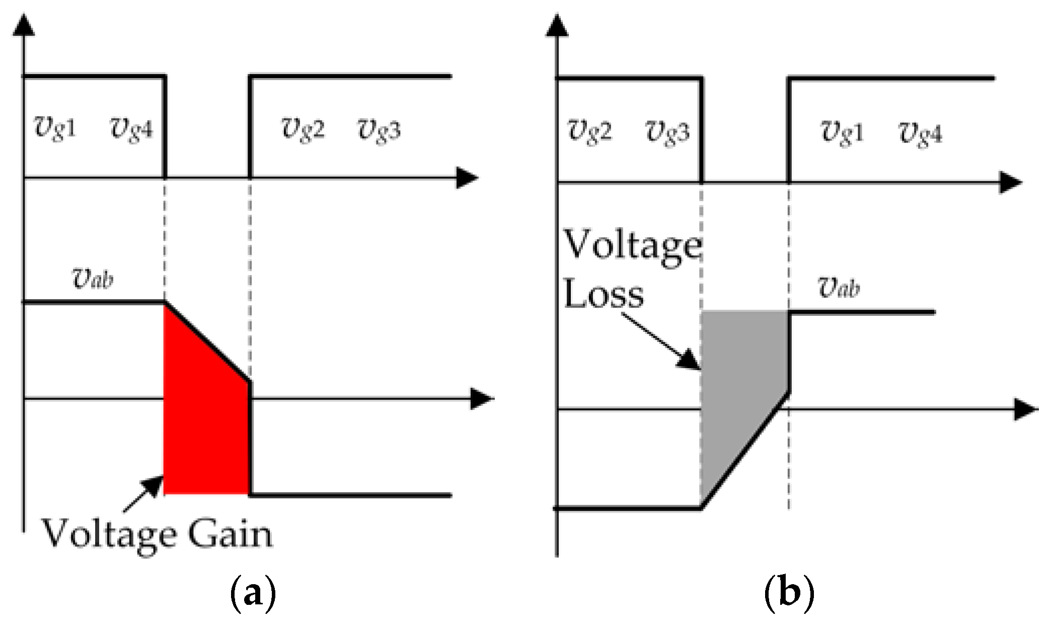
Figure 5 shows the pole voltage and voltage error in a switching cycle. The PTN commutation introduces positive voltage error, while the NTP commutation creates negative voltage error. The NZVS results in linear changing of
vab and AZVS results in nonlinear changing of
vab.
5. Experiment
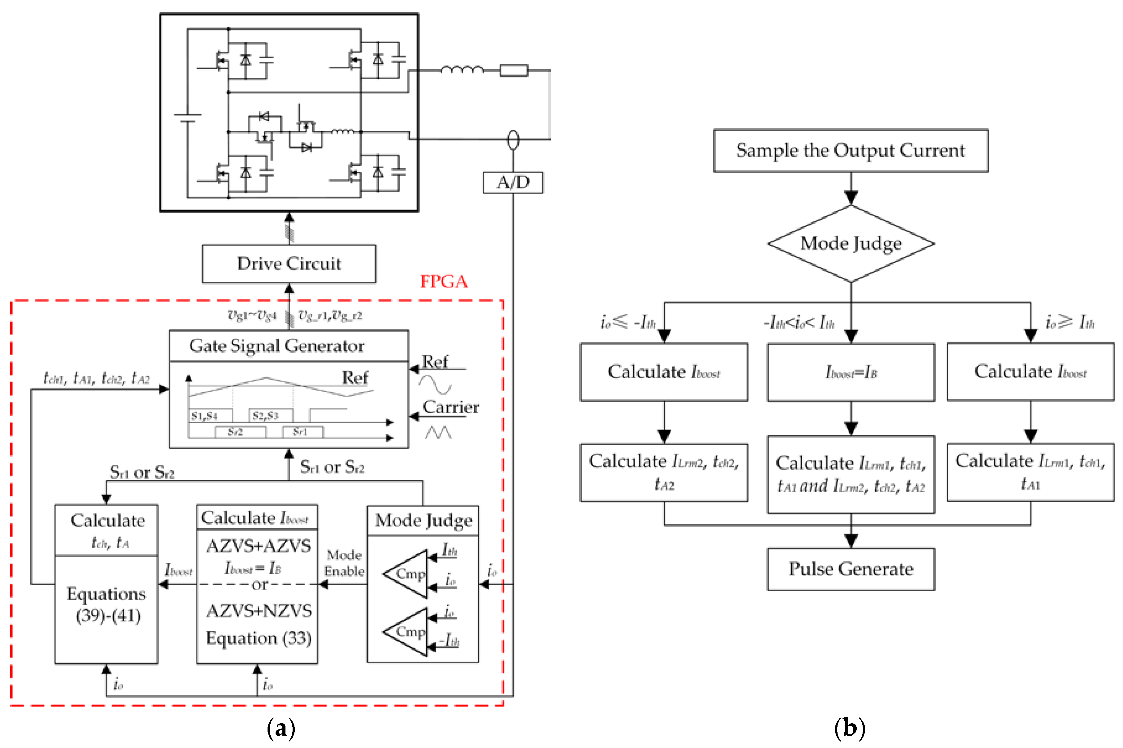
The proposed method was implemented in the Altera Cyclone IV FPGA with parameters in
Table 4.
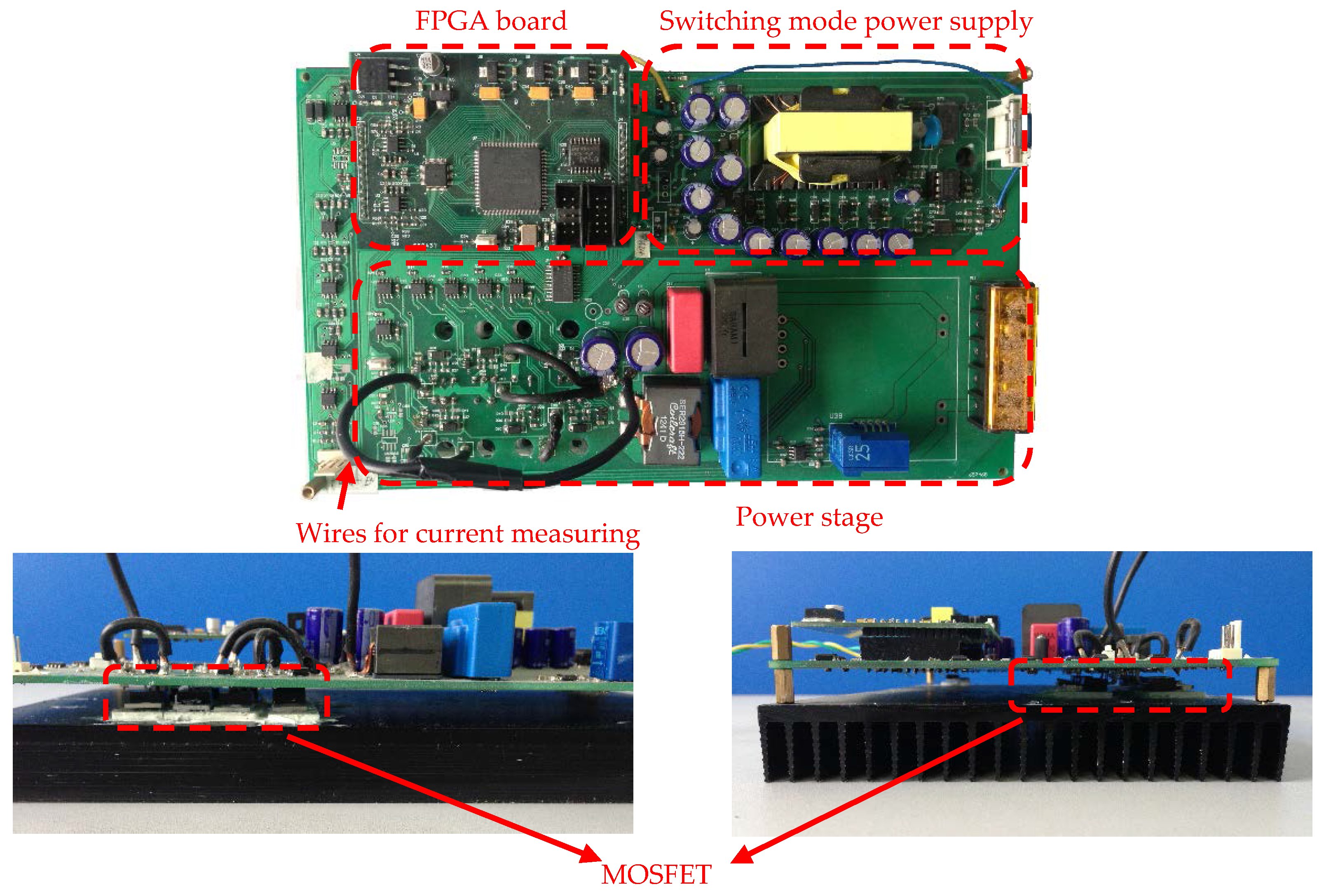
Figure 10 shows the photograph of the prototype. It consists of FPGA (Altera Corporation EP4CE22E22C7N, the USA) control board, switching power supply, MOSFET driver and the power circuit.
The dead-time effect leads to the nonlinearity of inverter, which introduces the baseband harmonics in the output voltage and current. In the experiment, the total harmonic distortion (THD) of output current and output voltage with different methods are compared to verify the effectiveness of the proposed control method. The oscilloscope MSO4034B with the probes TCP0030, TPP0500 and P5025 is used to measure the voltages and currents. The power analysis module DPO4PWR is used to analyze the THD of the current and voltage.
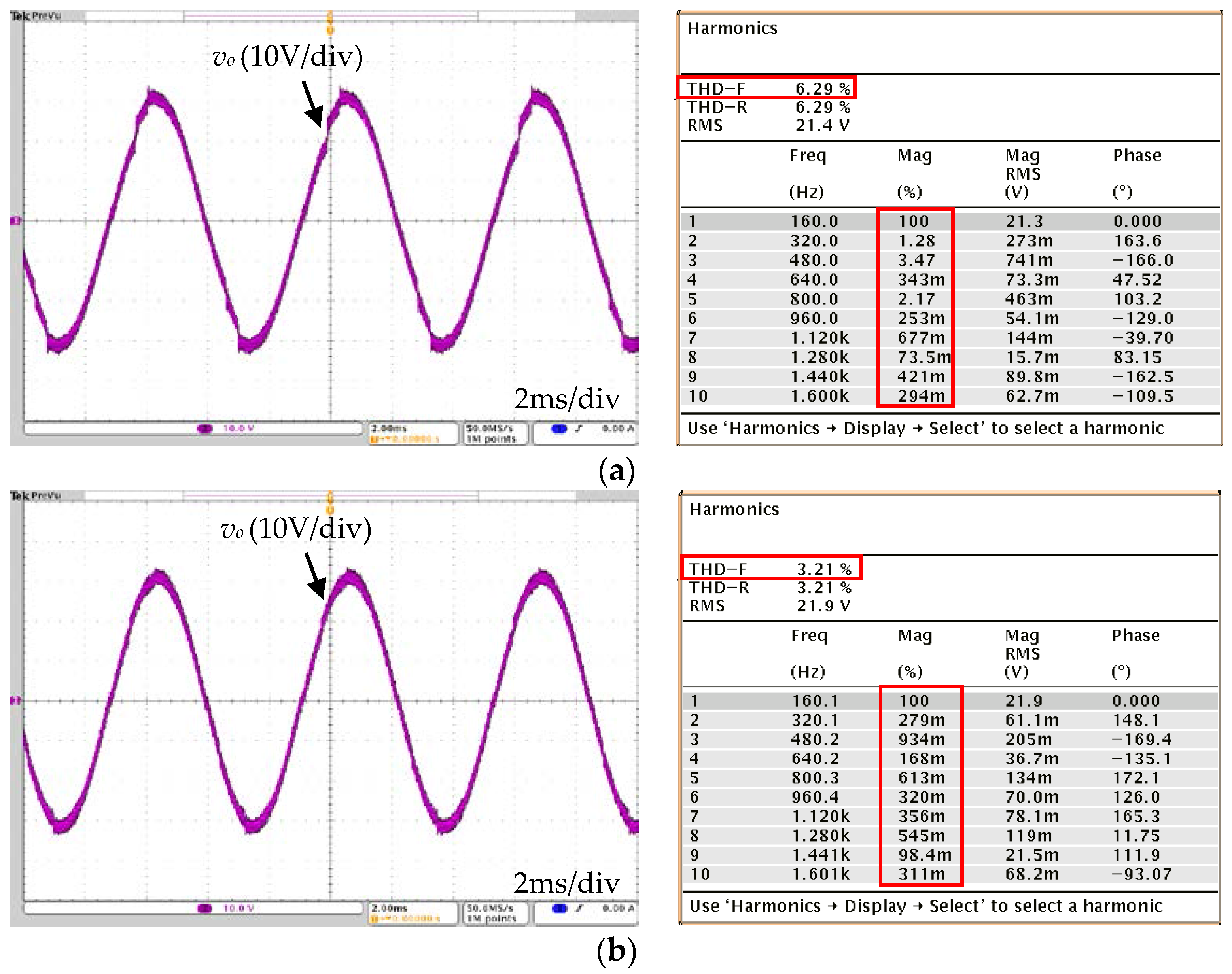
Figure 11 shows the voltage and current waveforms of ARSI with conventional variable-timing control and proposed control when the modulation index is 0.4 in an open-loop configuration. The auxiliary circuit is operated twice with bidirectional current in a switching cycle to realize the “AZVS + AZVS”. However, a single direction current occurs in the auxiliary circuit with realization of “NZVS + AZVS”. To measure the output voltage
vo, a filter is added to attenuate the carrier harmonics of the pole voltage
vab.
Figure 11a shows that a large voltage error occurs in the output voltage with conventional control due to the unequal commutation times. The distortion is obvious especially at the mode switching point between the “AZVS + AZVS” and “NZVS + AZVS”. The quality of the output voltage is improved with the proposed control in
Figure 11b. The voltage error with proposed control should be zero in theory. However, the voltage error exists in the experimental results due to the limited PWM resolution of 8 bit and current detecting error.
Figure 12 shows the voltage waveforms and their harmonic analysis results when the modulation index is 0.4 in an open-loop configuration. THD-F is the ratio of the RMS value of harmonic components to the RMS value of the fundamental component, while THD-R is the ratio of the RMS value of harmonic components to the RMS value of the source waveform. THD-F is used in the experiment to compare the quality of the voltage and current. The THD-F and magnitude of the harmonic voltages respect to the fundamental voltage are indicated by the red boxes in
Figure 12. THD-F of the output voltage with proposed control is 3.21%, which is less than 6.29% with conventional control. The magnitudes of the baseband harmonics are reduced by using the proposed control.
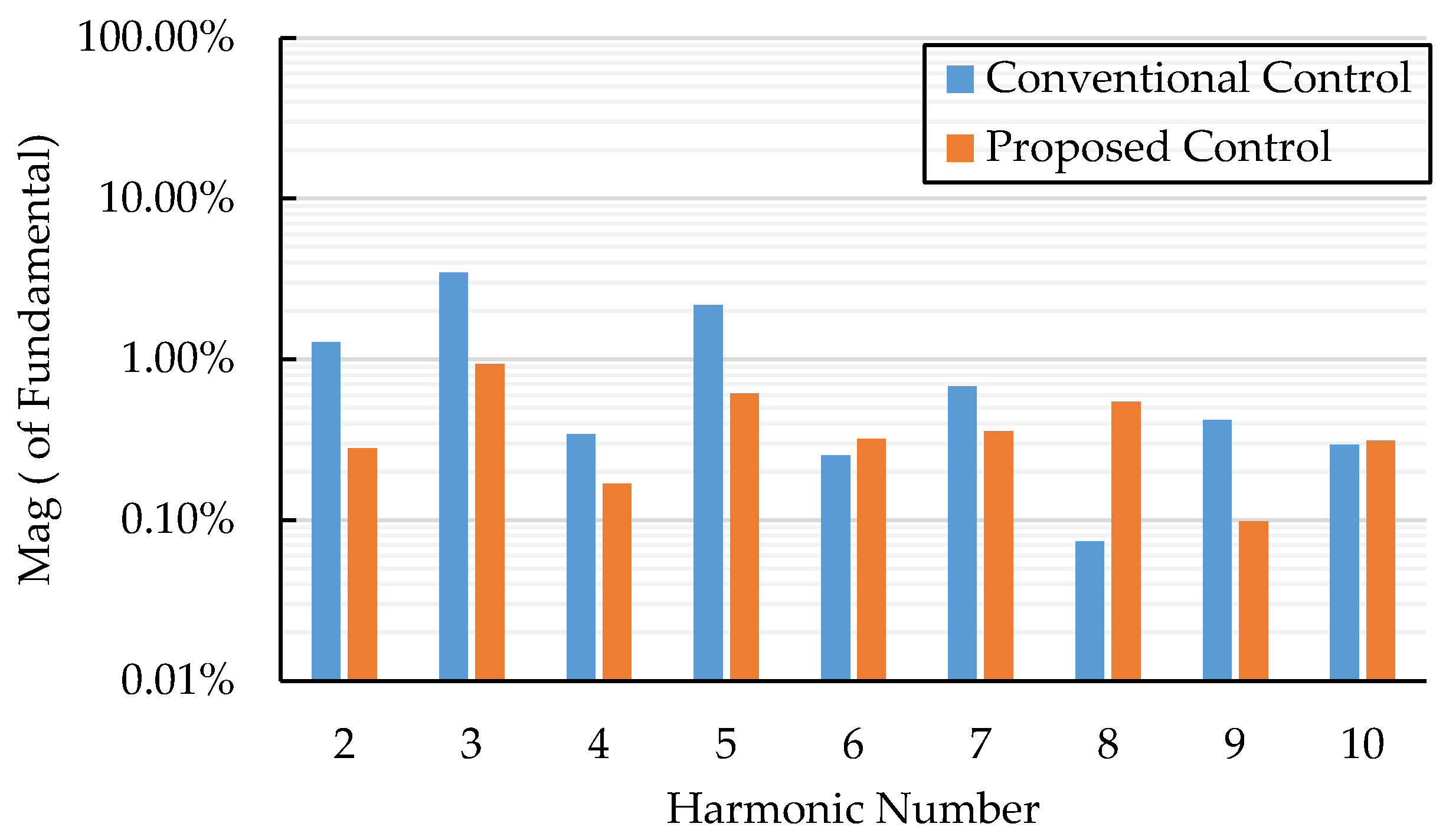
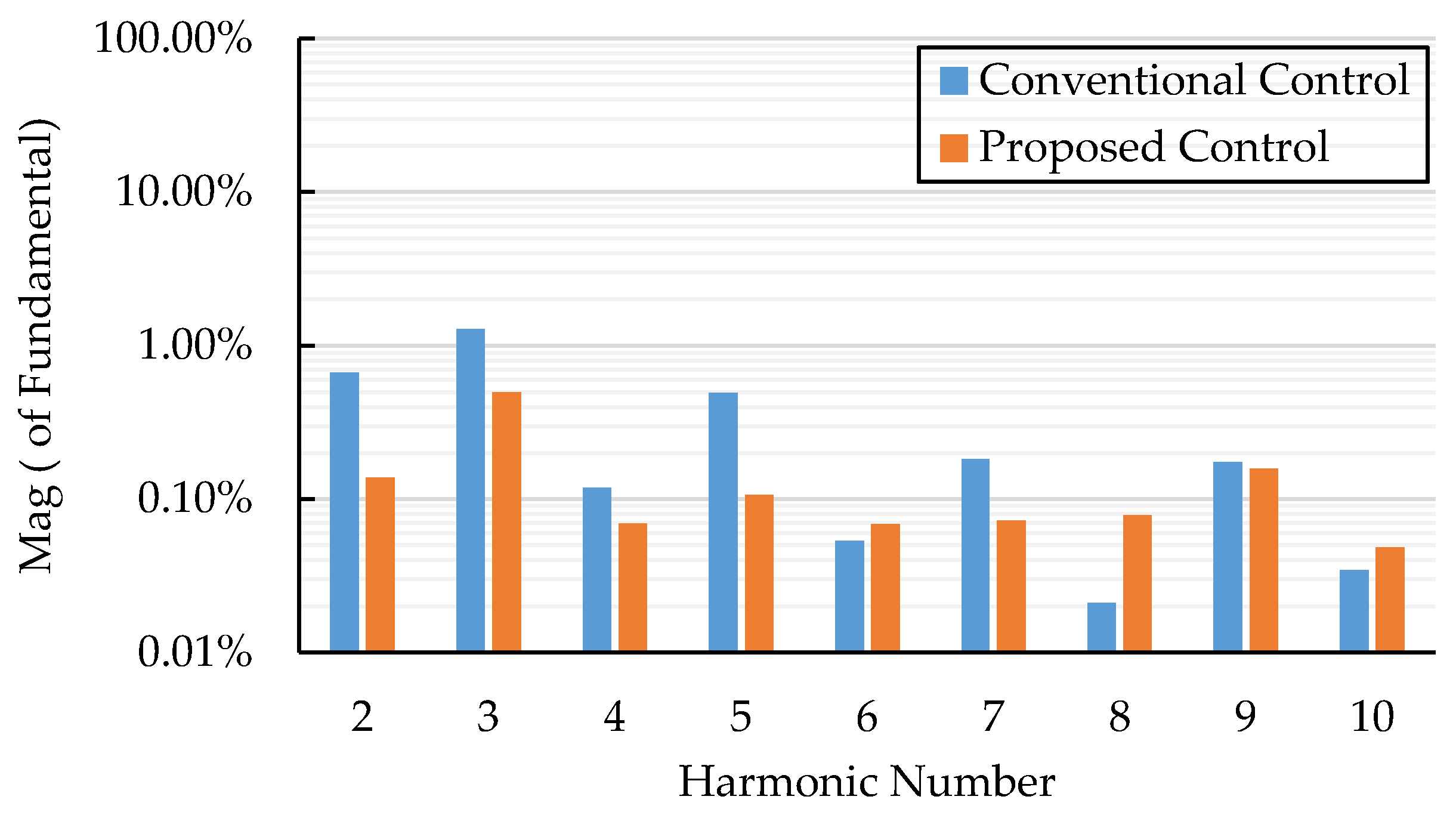
Figure 13 shows the magnitudes of the 2nd–10th harmonic voltages with respect to the fundamental voltage. The magnitudes of the harmonic voltages are reduced obviously with the proposed control, except the 6th, 8th and 10th harmonic currents.
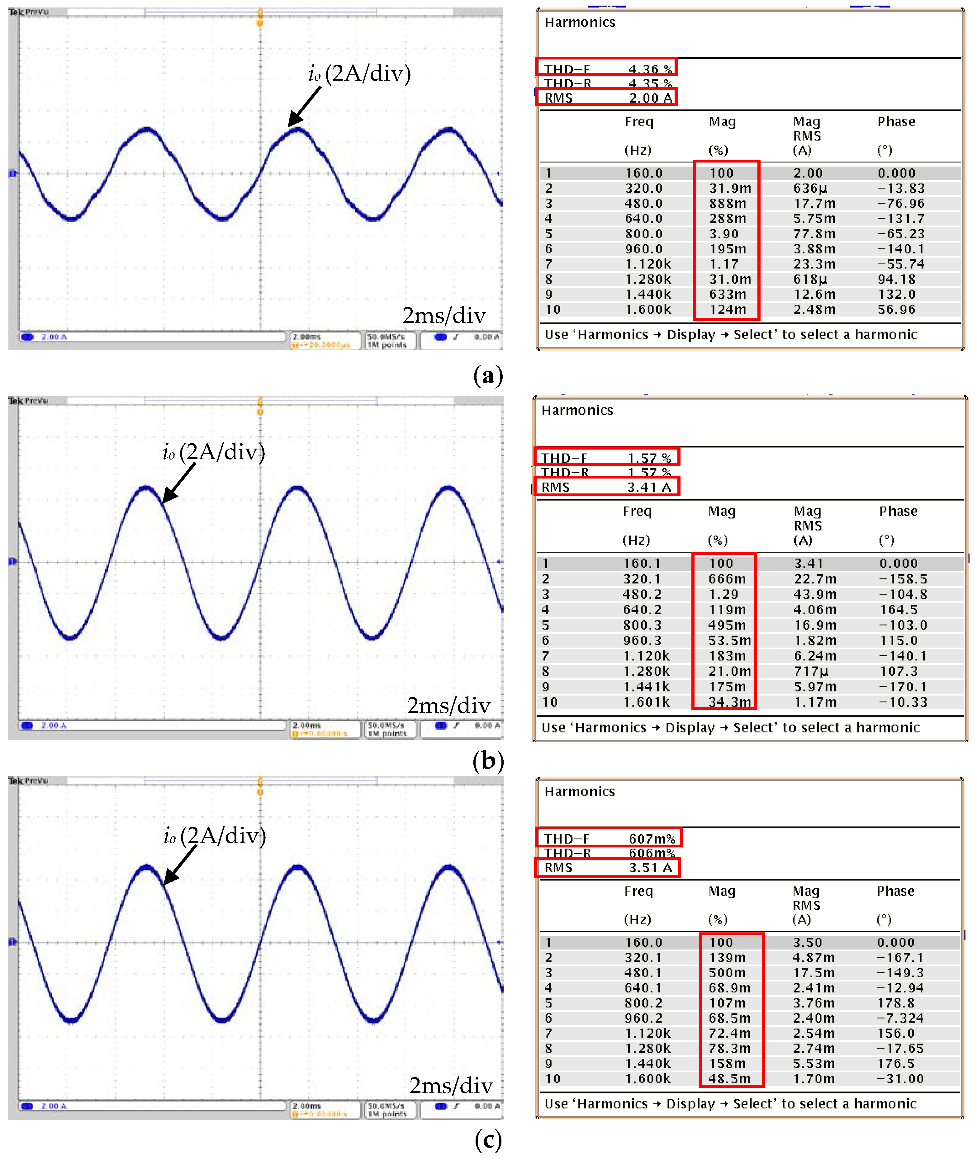
Figure 14 shows the current waveforms and their harmonic analysis results when the modulation index is 0.4 in an open-loop configuration. The THD-F, RMS and magnitude of the harmonic voltages with respect to the fundamental voltage are indicated by the red boxes. Due to a large dead time, severe distortion occurs in the output current of the hard-switching inverter, as shown in
Figure 14a. The RMS of the current is only 2A, which is much lower than the RMS of the soft-switching inverters with the modulation index 0.4. The THD-F of the hard-switching inverter is 4.36%. As for the ARSI, the THD-F is reduced to 1.57% and the RSM of the current is improved with conventional control, because the blanking delay error is eliminated which is the main error source in the hard-switching inverter. The THD-F of the output current is further improved to 0.607% by using the proposed control.
Figure 15 shows the magnitudes of the 2nd–10th harmonic currents of the ARSI respect to the fundamental current. The magnitudes of the harmonic currents are reduced obviously with the proposed control, except the 6th, 8th and 10th harmonic currents. The current results are in good agreement with the voltage results in
Figure 13.
6. Conclusions
This paper analyzed the dead-time effect of ARSI, which is a typical example of ZVT PWM inverters. The blanking delay error that is the main error source of the hard-switching inverter is eliminated in the ARSI. Only the error caused by the rise- and fall-times exist in the ARSI. For the dead-time effect, the PTN and NTP commutations, respectively, cause the positive and negative voltage errors that are proportional to the commutation time, regardless whether NZVS or AZVS of the main switches is realized. NZVS and AZVS determine the commutation time of the ARSI. Based on the analysis, a high-precision control has been proposed to eliminate the voltage error. In the experiment, the THD of the output current and voltage are greatly reduced from 1.57% and 6.29% to 0.607% and 3.21%, respectively, by using the proposed control. In conclusion, the output quality can be improved with the high-precision control method.
However, objectively speaking, there are still some disadvantages in the proposed control. This novel method improves the precision at the expense of efficiency, because of relatively higher auxiliary current compared with that of the traditional control. Besides, the current Iboost should be calculated online, resulting higher calculation effort.
Anyway, the proposed control is very attractive in the high-precision applications to improve the output quality. Despite the fact that the analysis and proposed control is based on the ARSI, they can be used similarly to other types of the ZVT PWM inverters to eliminate the dead-time effect.


