Article

Analytical Model for Voltage-Dependent Photo and Dark Currents in Bulk Heterojunction Organic Solar Cells

Department of Electrical and Computer Engineering, Concordia University, 1455 Blvd. de Maisonneuve West, Montreal, QC H3G 1M8, Canada
*
Author to whom correspondence should be addressed.
Energies 2016, 9(6), 412; https://doi.org/10.3390/en9060412
Submission received: 16 April 2016 / Revised: 13 May 2016 / Accepted: 14 May 2016 / Published: 26 May 2016
(This article belongs to the Special Issue Nano-Structured Solar Cells)

Abstract

:
A physics-based explicit mathematical model for the external voltage-dependent forward dark current in bulk heterojunction (BHJ) organic solar cells is developed by considering Shockley-Read-Hall (SRH) recombination and solving the continuity equations for both electrons and holes. An analytical model for the external voltage-dependent photocurrent in BHJ organic solar cells is also proposed by incorporating exponential photon absorption, dissociation efficiency of bound electron-hole pairs (EHPs), carrier trapping, and carrier drift and diffusion in the photon absorption layer. Modified Braun’s model is used to compute the electric field-dependent dissociation efficiency of the bound EHPs. The overall net current is calculated considering the actual solar spectrum. The mathematical models are verified by comparing the model calculations with various published experimental results. We analyze the effects of the contact properties, blend compositions, charge carrier transport properties (carrier mobility and lifetime), and cell design on the current-voltage characteristics. The power conversion efficiency of BHJ organic solar cells mostly depends on electron transport properties of the acceptor layer. The results of this paper indicate that improvement of charge carrier transport (both mobility and lifetime) and dissociation of bound EHPs in organic blend are critically important to increase the power conversion efficiency of the BHJ solar cells.

1. Introduction

Over the past decade, bulk heterojunction (BHJ) polymer solar cells based on blends of conjugated polymers and fullerene derivatives (e.g., P3HT:PCBM blend) have drawn a huge attention in research due to their high conversion efficiency, solution-based easy fabrication, and abundant availability [1,2]. Although presently BHJ cells show a reasonable power conversion efficiency (almost 10%), further efficiency improvements/optimizations seem very likely by better understanding the operating principles through accurate physics-based modeling and optimizations. A high binding energy of the bound electron-hole pairs (EHPs) due to low dielectric constant (εr) of organic materials reduces the number of photogenerated free carriers [3]. The photoionized electron and its twin hole (geminate pair) cannot immediately escape from their mutual columbic attraction and the geminate pair dissociates to free charge carriers with probability M. Then the free carriers drift across the photoconductor layer by the built-in electric field and some of the carriers are lost by deep trapping/recombination. At the optimum operating output voltage, the built-in electric field is decreased, which reduces the charge collection efficiency of the photogenerated carriers. Moreover, at the same time, the forward diode-like current (commonly known as the dark current) increases considerably. Both the photo and dark currents critically depend on the carrier transport properties of the blend (active layer) and cell structure. Thus the overall cell efficiency is mainly dominated by the photon absorption, dissociation efficiency of bound EHPs, charge collection efficiency and dark current. Therefore, an explicit physics-based model for the voltage-dependent photo and dark currents is highly desirable for enhancing the efficiency and optimizing the design.
The dominating loss factor in BHJ organic solar cells is one of the most debated topics in recent time. In early BHJ, the initial geminate recombination was the dominant loss mechanism [3]. The dissociation efficiency has been improved in some recent blends and becomes close to unity. For example, cells made of a blend of the conjugated polymer poly[N-9”-hepta-decanyl-2,7-carbazole-alt-5,5-(4’,7’-di-2-thienyl-2’,1’,3’-benzothiadiazole)] (PCDTBT) with the soluble fullerene derivative (PCBM) show nearly unity dissociation efficiency [4]. However, their cell efficiency strongly depends on the charge collection efficiency due to trapping/recombination of free carriers. Traditionally, bimolecular recombination processes in organic solar cells have been discussed extensively in the scientific literature and Shockley-Read-Hall (SRH) interface states at the bulk heterojunction has been considered, but largely discarded. Recently, however, Street et al. [5] concluded that recombination of mobile carriers at SRH-type interface states at or near the buried heterojunction is the dominant recombination mechanism. Shuttle et al. [6] showed that the bimolecular recombination coefficient depends on the charge carrier concentration in a way that the recombination coefficient becomes equivalent to the SRH-type trap-assisted recombination. Moreover, Mandoc et al. [7] showed that, for 1 sun intensity or less, the SRH-type recombination dominates over the bimolecular recombination. Therefore, for simplicity, the trap-assisted (first order) monomolecular recombination is considered in this paper.
In our previous publication [8], we developed an explicit expression for the photocurrent in BHJ cells by incorporating exponential photon absorption, dissociation efficiency of bound EHPs, carrier trapping/recombination, carrier drift and diffusion, and actual solar spectrum. The previous model [8] ignored the contact effects. The Fermi positions at the two metal contacts are fixed by the metal work functions and thus the charge carrier concentrations at the contacts remain the same irrespective of the operating output voltage [9]. In this paper, the previous analytical model for the photocurrent has been modified by solving the continuity equations for both electrons and holes with proper boundary conditions.
The dark current versus voltage behavior has a significant effect on the overall current-voltage characteristics of the cell. Though the common diode equation has been used for the dark current, its validity in BHJ solar cells has not yet been justified [5]. Kumar et al. [10] proposed an analytical expression for the dark current considering carrier drift and diffusion across the active layer. Since there exists quasi Fermi levels all over the active layer, the recombination current should be the dominant dark current mechanism in BHJ solar cells.
In this paper, we have developed a physics-based mathematical model for the external voltage-dependent forward dark current by considering SRH recombination in the active layer. We also compare the model calculations with the published experimental results on the dark current behavior. Modified Braun model [11], which shows good agreement with the exact extension of Onsager theory except at extremely high electric field, is incorporated in the model to determine the dissociation of the bound EHPs. The analytical model is then compared with the published experimental results in order to determine the carrier transport properties. We examine the effects of the contact properties, blend compositions, charge carrier transport properties, and cell design on the current-voltage characteristics.

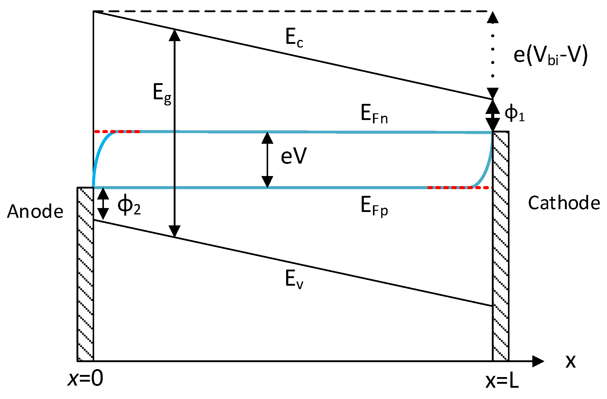
2. Theoretical Model

2.1. Dark Current

The active layer or blend layer is contacted by two metals: one of high work function, φ a (anode) and the other one of low work function, φ c (cathode). At thermal equilibrium, the energy band bends to make the Fermi level flat. Once there exists an external voltage across the structure, the tilting of the band is reduced and this voltage creates a separation of Fermi levels which we call quasi-Fermi levels as shown in Figure 1. The work function difference is called the built-in potential,
e V b i = φ a φ c = E g φ 1 φ 2
where e is the elementary charge and Vbi is the built-in potential.
The free electrons in the active layer travel through the acceptor towards the back contact whereas the holes remain in the donor and travel towards the light-receiving electrode (top contact). The free carriers move by the drift and diffusion mechanisms. The built-in electric field in the active layer assists the drift process. Hernandez-Garcia et al. [12] showed that the electric field is almost uniform across the active layer if the layer thickness is in the range of few hundreds nm or less. In fact, the optimum active layer thickness for the BHJ photovoltaics is 70–200 nm [4,13]. Therefore, the electric field F is considered uniform across the active layer. The drift mobility (μ) and carrier lifetime (τ) of holes and electrons are also considered uniform to allow the problem to be analytically tractable [9].
Considering the assumptions mentioned above, the steady-state continuity equation for electrons is:
μ n F d n ( x ) d x + D n d 2 n ( x ) d x 2 + G R n = 0
where n is the electron concentration, G is the carrier generation rate, Rn is the recombination rate (=rmn(x) = n(x)/τn; where rm is the monomolecular recombination coefficient and τn is the electron lifetime), F is the electric field, μn and Dn are the electron mobility and electron diffusion coefficient, respectively. The diffusion coefficient is assumed to be independent of n and can be determined using Einstein’s relation, Dnn = kT/e = Vt. The electric field can be written as:
F = V V b i L
where V is the external voltage, L is the entire active layer thickness and Vbi can be calculated from Equation (1).
Under dark condition (G = 0), Equation (2) becomes,
d 2 n ( x ) d x 2 + F V t d n ( x ) d x n ( x ) L n 2 = 0
where Ln (= D n τ n ) is the diffusion length of electrons.
The solution of Equation (4) is:
n ( x , V ) = A 1 exp ( m 1 x ) + A 2 exp ( m 2 x )
where,
m 1 , 2 = F 2 V t ± ( F 2 V t ) 2 + 1 L n 2
The Fermi positions at the two contacts in the photoconductor layer are determined by the metal work functions. Thus, the constants A1 and A2 can be determined by the following two boundary conditions:
n ( 0 ) = N c exp ( E g φ 2 e V t ) ,   and   n ( L ) = N c exp ( φ 1 e V t )
where Nc is the effective density of states in the conduction band.
The expressions of A1 and A2 are:
A 1 = N c [ exp ( E g φ 2 e V t + m 2 L ) exp ( φ 1 e V t ) ] exp ( m 2 L ) exp ( m 1 L )
A 2 = N c [ exp ( φ 1 e V t ) exp ( E g φ 2 e V t + m 1 L ) ] exp ( m 2 L ) exp ( m 1 L )
Similarly, the expression of holes under dark condition is:
p ( x , V ) = B 1 exp ( k 1 x ) + B 2 exp ( k 2 x )
where,
k 1 , 2 = F 2 V t ± ( F 2 V t ) 2 + 1 L p 2   and   L p = D p τ p
The boundary conditions for holes are:
p ( 0 ) = N v exp ( φ 2 e V t )   and   p ( L ) = N v exp ( E g φ 1 e V t )
where Nv is the effective density of states in the valence band.
Applying the above boundary conditions, the constants B1 and B2 are,
B 1 = N v [ exp ( φ 2 e V t + k 2 L ) exp ( E g φ 1 e V t ) ] exp ( k 2 L ) exp ( k 1 L )
B 2 = N v [ exp ( E g φ 1 e V t ) exp ( φ 2 e V t + k 1 L ) ] exp ( k 2 L ) exp ( k 1 L )
It is obvious from Figure 1 that the quasi-Fermi levels for both electrons (EFn) and holes (EFp) coincide with each other at the contacts, yet in most part of the blend thickness the difference remains the same, i.e., EFnEFpeV. For simplicity, if we consider EFnEFpeV throughout the active layer, then the electron and hole profiles can be simplified as:
n ( x , V ) = n i exp ( E g 2 φ 2 2 e V t ) exp ( V V t ) exp ( V b i V L V t x )
and   p ( x , V ) = n i exp ( E g 2 φ 2 2 e V t ) exp ( V b i V L V t x )
where ni is the intrinsic carrier concentration in the blend.
Setting V = 0 (i.e., at the short circuit condition) in Equations (5) and (10) or in Equations (15) and (16), the electron and hole profiles become:
n 0 ( x ) = n i exp ( E g 2 φ 2 2 e V t ) exp ( V b i L V t x )
and   p 0 ( x ) = n i exp ( E g 2 φ 2 2 e V t ) exp ( V b i L V t x )
The dark current due to the SHR recombination can be written as:
J d a r k = J r e c = e 0 L R ( x ) d x
where,
R = n p n i 2 τ p ( n + n i ) + τ n ( p + n i )
For simplicity, the trap levels are assumed to be near the middle of the bandgap in Equation (20). Note that one has to substitute the values of n and p from Equations (5) and (10) into Equation (19) and perform numerical integration of Equation (19) in order to calculate the dark current, Jdark. However, as shown in Figure 1, holes are the majority carrier in the first half of the active layer and electrons are the majority carriers in the other half. Thus, R ≈ (n - n0)/τn for x = 0 to L/2 provided φ 1 φ 2 . Therefore, an analytical expression of the dark current due to the SHR recombination can be determined as:
J d a r k = e 0 L / 2 n ( x , V ) n 0 ( x ) τ n d x + e L / 2 L p ( x , V ) p 0 ( x ) τ p d x = J r n + J r p
where,
J r n = e τ n [ A 1 m 1 { exp ( m 1 L 2 ) 1 } + A 2 m 2 { exp ( m 2 L 2 ) 1 } n i L V t V b i exp ( E g 2 φ 2 2 e V t ) { exp ( V b i 2 V t ) 1 } ]
and
J r p = e τ p [ B 1 k 1 { exp ( k 1 L ) exp ( k 1 L 2 ) } + B 2 k 2 { exp ( k 2 L ) exp ( k 2 L 2 ) } n i L V t V b i exp ( E g 2 φ 1 2 e V t ) { exp ( V b i 2 V t ) 1 } ]
Again, if we replace n(x,V) and p(x,V) in Equation (19) by their approximate formulii n′(x,V) and p′(x,V) from Equations (15) and (16), we can get the following compact expression of the dark current:
J d a r k = e n i exp ( E g 2 e V t ) [ 1 τ n exp ( φ 2 e V t ) + 1 τ p exp ( φ 1 e V t ) ] ×         [ L V t V b i V exp ( V V t ) { exp ( V b i V 2 V t ) 1 } L V t V b i { exp ( V b i 2 V t ) 1 } ]
As evident from Equation (24), the dark current is almost inversely proportional to the carrier lifetimes and it exponentially increases with increasing the injection barrier heights ( ϕ 1 and ϕ 2 ).

2.2. Dissociation Efficiency

Braun [14] proposed an empirical model to compute electric field-dependent escape probability, assuming geminate recombination at a nonzero reaction radius. Reaction radius is the minimum distance required between bound the electron and hole to recombine. The expression for electric field-dependent dissociation rate proposed by Braun is [15]:
M ( F ) = K d ( F ) K d ( F ) + K f
where F is the electric field, M is the escape probability, Kd is the separation rate, Kf (= S/r0) is the recombination rate of bound EHPs, r0 is the initial separation between a bound EHP, S is the reactivity parameter. Reactivity parameter is the relative velocity between bound electron and hole at the reaction radius. Wojcik et al. [11] have showed that Modified Braun model agrees well with the exact extension of Onsager theory except at extremely high fields. According to the Modified Braun’s model [11]:
K d ( F ) = D r c r 0 3 e r c r 0 J 1 ( 2 2 b ) / 2 b
Thus Equation (25) becomes:
M ( F ) = [ 1 + K f r 0 3 e r c r 0 D r c J 1 ( 2 2 b ) / 2 b ]
where D is the sum of the diffusion coefficients of electrons and holes in respective mediums, rc (= e 2 / 4 π ε o ε r k T ) is the Onsager radius, J1 is the first order Bessel function, ε o ε r is the effective dielectric constant of the blend, e is the elementary charge, k is the Boltzmann constant, T is the absolute temperature, and the reduced field, b = e 3 F / 8 π ε o ε r k 2 T 2 .

2.3. Photocurrent

The incident photons are absorbed in the active layer and free EHPs are created there. The photogenerated electrons travel through the acceptor towards the back contact whereas the holes remain in the donor and travel towards the radiation-receiving electrode (top contact). The EHP generation rate (G) in the blend layer can be expressed as [16]:
G ( λ , V ) = α ( λ ) [ 1 R ( λ ) ] λ I 0 ( λ ) M / h c
where I0 is the intensity of the solar spectra (W/cm2-nm), c is the speed of light, h is the Plank constant, R is the reflectance or the loss factors, α(λ) is the absorption coefficient of the blend and λ is the incident photon wavelength.
The photogenerated excess electron concentration can be determined by solving the following steady-state the continuity equation:
μ n F x ( δ n ) + D n 2 x 2 ( δ n ) + G e α ( λ ) x δ n τ n = 0
where δn is the photogenerated electron concentration.
The solution of Equation (29) is:
δ n ( x , λ ) = C 1 exp ( m 1 x ) + C 2 exp ( m 2 x ) + A exp [ α ( λ ) x ]
Since the carrier concentrations at the two boundaries are fixed, the boundary conditions for the photogenerated excess carriers are δn(0) = δn(L) = δp(0) = δp(L) = 0, where δp is the photogenerated hole concentration. Applying these two boundary conditions, the expressions of C1 and C2 are:
C 1 = A [ exp ( α L ) exp ( m 2 L ) ] exp ( m 2 L ) exp ( m 1 L )
and   A = G τ n 1 αμ n F τ n ( L n α ) 2
C 2 = A [ exp ( α L ) exp ( m 1 L ) ] exp ( m 1 L ) exp ( m 2 L )
The photocurrent density due to electrons that are travelling towards the back electrode, is [8,17]:
J n ( λ , V ) = e L μ n F 0 L δ n d x   = e L μ n F { C 1 m 1 [ exp ( m 1 L ) 1 ] + C 2 m 2 [ exp ( m 2 L ) 1 ] A α [ exp ( α L ) 1 ] }
Similarly, the photocurrent density for hole transport is:
J p ( λ , V ) = e L μ p F { D 1 k 1 [ exp ( k 1 L ) 1 ] + D 2 k 2 [ exp ( k 2 L ) 1 ] B α [ exp ( α L ) 1 ] }
where,
D 1 = B [ exp ( α L ) exp ( k 2 L ) ] exp ( k 2 L ) exp ( k 1 L )
D 2 = B [ exp ( α L ) exp ( k 1 L ) ] exp ( k 1 L ) exp ( k 2 L )
B = G τ p 1 αμ p F τ p ( L p α ) 2
The photocurrent density due to the incident radiation can be obtained by integrating over all incident photon wavelengths of the solar spectrum, i.e.:
J p h ( V ) = 0 { J n ( λ , V ) + J p ( λ , V ) } d λ

2.4. Net External Current

The net external current density from a solar cell is [18]:
J ( V ) = J d a r k ( V ) + V J R s R p J p h ( V )
where Rs and Rp are the series and shunt area resistances, respectively. Therefore, the expression of the electric field (Equation (3)) has to be modified to F = ( V J R s ) V b i L and V has to be replaced by (VJRs) in all expressions above for the calculation of the external current.

3. Results and Discussion

We explicitly examine both the dark and net (sum of the dark and photocurrent) current behaviors as a function of the external voltage in BHJ organic solar cells by comparing the model calculations with recently published experimental results. The various parameters of the P3HT:PC61BM BHJ organic solar cells are given in Table 1. The effective bandgap is the difference between acceptor LUMO (lowest unoccupied molecular orbital) level and donor HOMO (highest occupied molecular orbital) level. Unless otherwise stated, the parameters shown in Table 1 are the fixed parameters used in all model calculations.

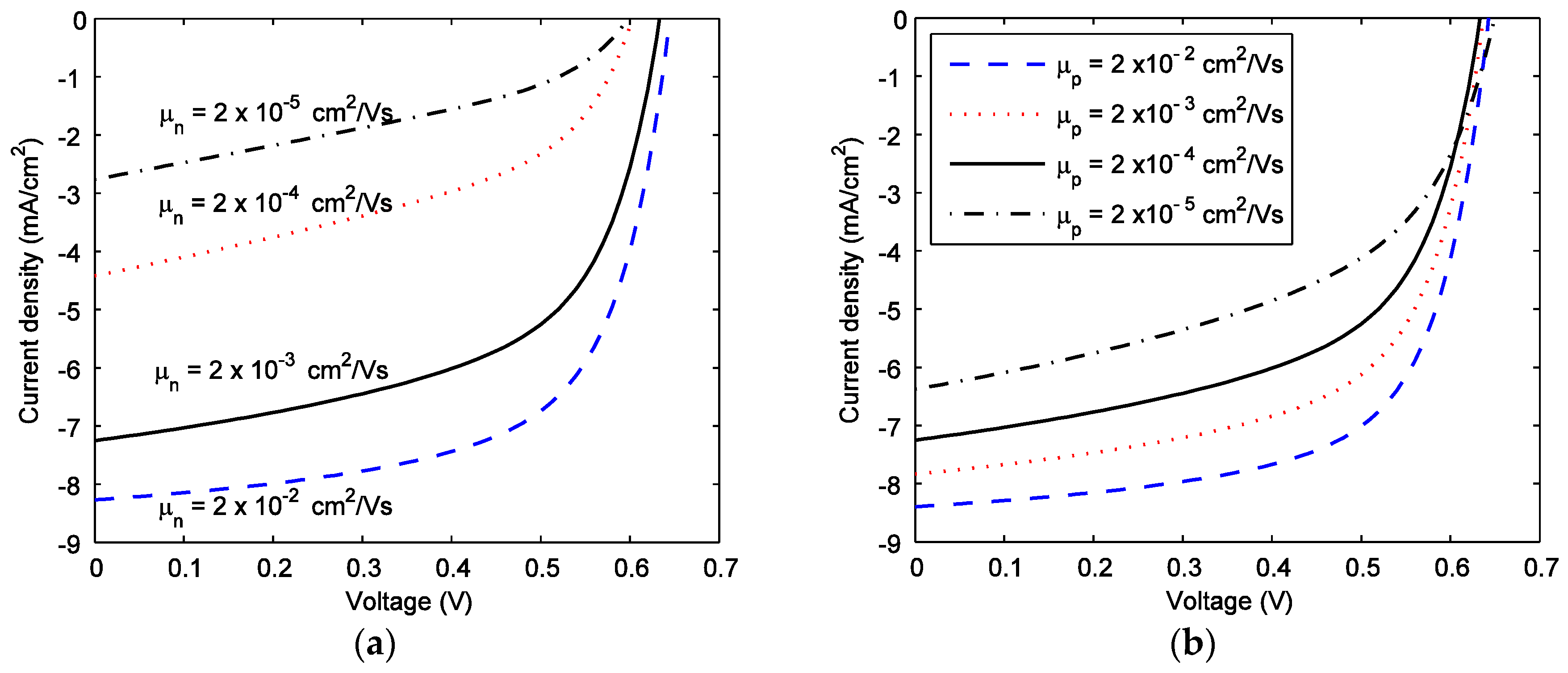
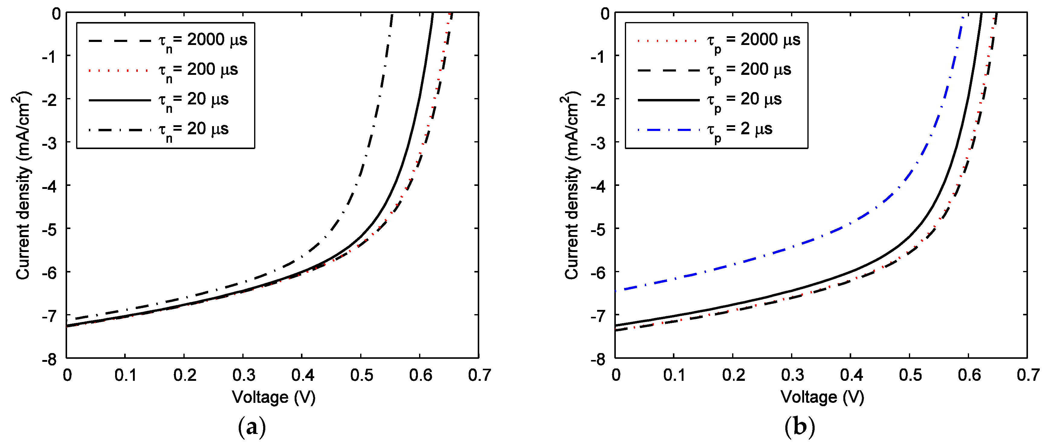
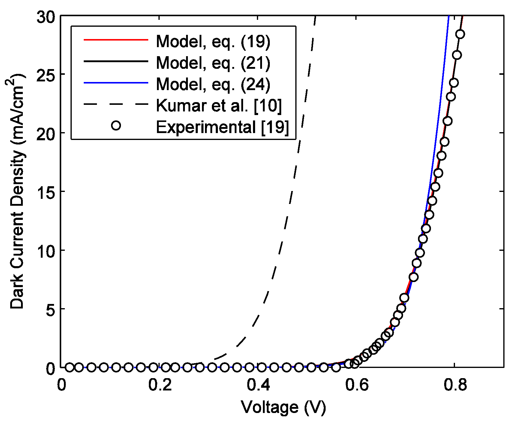
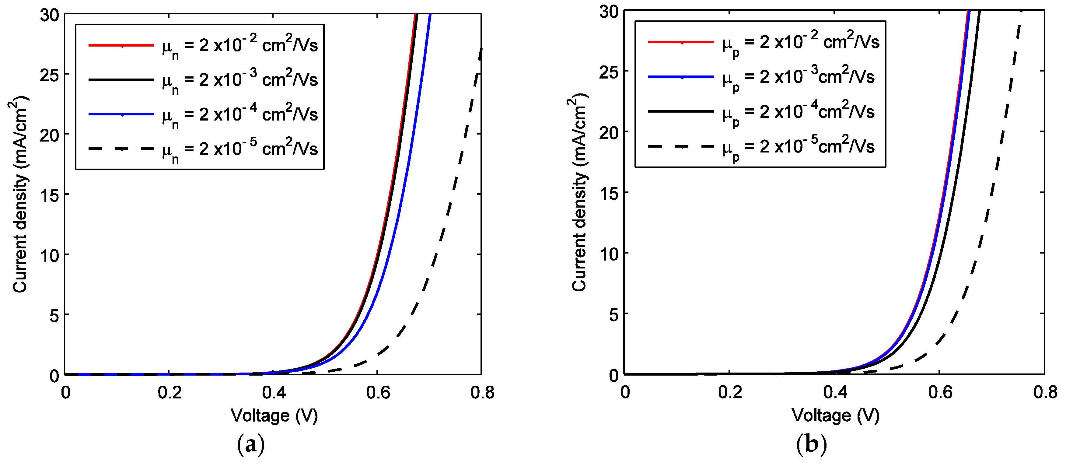
3.1. Dark Current Density

Figure 2a,b shows the dark current versus external voltage of a P3HT:PC61BM solar cell. The experimental data are extracted from References [19,20]. The active layer thickness, L = 200 nm [19]. The symbols, dashed, and solid lines represent experimental results, drift-diffusion model of Kumar el al. [10], present model fit to experimental data, respectively. As evident from Figure 2, the dark current models considering the SRH recombination provide better fittings. The dark current calculations using Equations (19) and (21) are almost identical because of symmetrical carrier profile across the active layer ( ϕ 1 = ϕ 2 ). The best fitted parameters in Figure 2 are; µp = 2 × 10⁻⁴ cm2/Vs, µn = 2 × 10⁻³ cm2/Vs, Rs = 1 Ω·cm2. The carrier lifetimes, τn = τp = 3 and 6 μs in Figure 2a,b, respectively. The drift-diffusion model of Kumar el al. [10] shows much higher dark current than the experimental results.
The dark current as a function of the external voltage of a PTB7:PC71BM (poly[[4,8-bis[(2-ethylhexyl)oxy]benzo[1,2-b:4,5-b′]dithiophene-2,6-diyl][3-fluoro-2-[(2-ethyl-hexyl)carbonyl]thieno [3,4-b]thiophenediyl]]) solar cell is shown in Figure 3. The experimental data are extracted from Reference [19]. Similar to P3HT:PC61BM solar cell, the SRH recombination is the main source of dark current in PTB7:PC71BM solar cells. The best fitted values of carrier lifetimes are τn = τp = 45 μs. All other parameters in Figure 3 are the same as in Figure 2. Since the results using Equations (19) and (21) are almost identical and show the best fit to the experimental data, Equation (21) is used for calculating the dark current in the rest of this paper.
The dark current is almost inversely proportional to the carrier lifetimes and it exponentially increases with increasing the injection barrier heights as evident from Equations (21) and (24). However, the effects of carrier mobilities on the dark current are not explicitly understandable from these equations. Therefore, it is instructive to show their effects through model calculations. The effects of carrier mobilities on the dark current in P3HT:PCBM solar cells are shown in Figure 4. All the parameters in Figure 4 are the same as in Figure 2. The dark current slightly decreases with decreasing the carrier mobility up to 10−4 cm2/Vs whereas it decreases abruptly by reducing the mobility below 10−4 cm2/Vs.

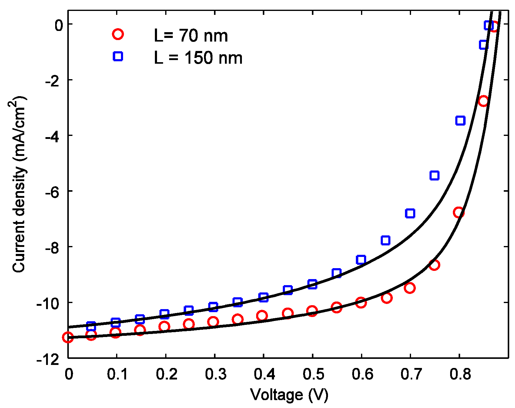
3.2. Net External Current

The absorption coefficients of the blends (PCDTBT:PC70BM and P3HT:PC61BM) at different wavelengths are taken into account [21,22]. The carrier lifetimes are kept within an acceptable range while fitting the experimental results [5,23]. Figure 5 shows the J-V curves of P3HT:PCBM solar cells at different sun intensities (i.e., 0.5, 0.75, 1 and 1.4 sun) for L = 230 nm. The symbols represent experimental data, and the solid lines represent the model fit to the experimental results. The experimental data for different sun intensities are extracted from Figure 4a of Reference [13]. The exciton dissociation efficiency at the operating voltage is about 87% for r0 = 1.5 nm. In order to ensure the best fit to the experimental results, the electron and hole lifetimes are kept fixed at 2 μs and 18 μs, respectively. The values of other fitting parameters in Figure 2 are; µp = 5 × 10⁻⁴ cm2/Vs, µn = 5 × 10⁻³ cm2/Vs, Rs = 0.3 Ω·cm2, and R = 0.11. The power conversion efficiency for 1 sun intensity is 2.87%. The analytical model agrees well with the experimental data.
Figure 6 shows the effects of active layer thickness on J-V characteristics of PCDTBT:PC71BM solar cells. The symbols and solid lines represent the experimental results [4] and model fit, respectively. The cell performance, particularly the fill factor, deteriorates with increasing the active layer thickness from 70 to 150 nm. Low carrier mobility in PCDTBT are responsible for lower charge collection efficiency in thicker devices. Therefore, the active layer thickness is usually kept around 70–80 nm. The bandgap and dielectric constant (εr) of PCDTBT:PCBM blend are 1.2 eV and 3.8. The dissociation efficiencies at maximum power points are 99% and 98.5% for W = 70 nm and W = 150 nm, respectively, which indicates that the dissociation efficiency in PCDTBT:PCBM blend is much higher as compared to P3HT:PCBM blend. The other fitting parameters in Figure 6 are; μn = 5 × 10⁻⁵ cm2/Vs, μp = 6 ×10⁻⁵ cm2/Vs, τn = 13 μs, τp = 25 μs, r0 = 1.8 nm, and Rs = 0.3 and 1 Ω·cm2 for W = 70 and 150 nm, respectively. The fill factor decreases from 67.8% to 55% by increasing the active layer thickness from 70 nm to 150 nm.
The effect of blend thickness (L) on short circuit current density (Jsc) for a P3HT: PCBM based BHJ solar cell is shown in Figure 7. The symbols and solid lines represent the experimental data and the model fit to the experimental results, respectively. The experimental data are extracted from Figure 6 of Reference [24]. The short circuit current should increase with increasing the blend thickness because the thicker layer absorbs more photons (i.e., higher quantum efficiency). On the other hand, the charge collection efficiency decreases with increasing the thickness, which results in lower short circuit current. Thus, there exists an optimum thickness that maximizes the short circuit current as shown in Figure 7. The fitting parameters in Figure 7 are; μn = 10−3 cm2/Vs, μp = 2 × 10⁻⁴ cm2/Vs, τn = 0.1 μs, τp = 0.2 μs, R = 0.02, and Rs = 0.5 Ω·cm2.
The injection barrier heights have a profound effect on the current-voltage characteristics of organic solar cells. The effects of the injection barriers on the current-voltage characteristics of P3HT:PCBM based BHJ solar cells are shown in Figure 8. An increase of the electron (hole) injection barrier is equivalent to an increase (decrease) of the cathode (anode) work functions. The built-in potential and electric field decrease with increasing the injection barriers, which reduces the charge collection. Therefore, the short circuit current decreases almost linearly with increasing the barrier heights. The open circuit voltage slighty decreases with increasing the barrier heights for low barrier heights ( ϕ 1 , ϕ 2 < 0.3 eV) and it is equal to the built-in potential for the higher barriers ( ϕ 1 , ϕ 2 ≥ 0.4 eV). The parameters used in Figure 8 are; μn = 2 × 10⁻³ cm2/Vs, μp = 2 × 10⁻⁴ cm2/Vs, τn = τp = 20 μs, L = 180 nm, R = 0, and Rs = 0.3 Ω·cm2.
The theoretical net current versus voltage characteristics of P3HT:PCBM solar cells by varying carrier mobilities are shown in Figure 9. All other parameters in Figure 9 are the same as in Figure 8. The short circuit current decreases drastically with decreasing both electron and hole mobilities, though the electron mobility affects the performance more severely. The open circuit voltage also decreases with decreasing the electron mobility. The hole mobility has comparatively less significant effect on the open circuit voltage. Both the dark and photo currents increase with increasing the carrier mobilities. The enhancement of the photocurrent with improved carrier mobility is higher than that of the dark current, and thus, the net current increases with increasing carrier mobilities.
Most of the incident photons are absorbed near the front contact (x = 0) and thus the photogenerated free electrons have to travel relatively longer distance than the photogenerated holes. Therefore, the efficiency of BHJ solar cells should be more prone to the electron lifetime than to the hole lifetime. The effects of τn and τp on the J-V characteristics of a 230 nm thick P3HT:PCBM solar cell are shown in Figure 10a,b, respectively. All other parameters in Figure 10 are the same as in Figure 8. The open circuit voltage and short circuit current decrease with decreasing both the electron and hole lifetimes. However, the open circuit voltage is more prone to the electron lifetime whereas the short circuit current is more prone to the hole lifetime. The enhancement of the dark current with decreasing carrier lifetimes reduces the open circuit voltage.

4. Conclusions

In this paper, physics-based mathematical models for the external voltage-dependent forward dark current and photocurrent of BHJ organic solar cells have been developed. The mathematical models are verified by comparing the model calculations with various published experimental results. The effects of the contact properties, blend compositions, charge carrier transport properties (carrier mobility and lifetime), and cell design on the current-voltage characteristics have been analyzed. The power conversion efficiency of BHJ organic solar cells mostly depends on electron transport properties (both the mobility and lifetime) of the acceptor layer.

Acknowledgments

The authors acknowledge the financial support from NSERC (Natural Science and Engineering Research Council of Canada) through its Discovery Grant program.

Author Contributions

The manuscript was prepared with contributions from all authors. Kabir conceived and supervised the work and had major contribution in the writing and organizing of the manuscript. Saleheen derived the theoretical model and performed all the calculations. Saleheen and Arnab developed the computer programming codes.

Conflicts of Interest

The authors declare no conflict of interest.

References

  1. Kumar, P.; Gaur, A.A. Model for the J-V characteristics of degraded polymer solar cells. J. Appl. Phys. 2013, 113, 094505. [Google Scholar] [CrossRef]
  2. Zhang, T.; Birgersson, E.; Luther, J. A spatially smoothed device model for organic bulk heterojunction solar cells. J. Appl. Phys. 2013, 113, 174505. [Google Scholar] [CrossRef]
  3. Mihailetchi, V.D.; Koster, L.J.A.; Hummelen, J.C.; Blom, P.W.M. Photocurrent Generation in Polymer-Fullerene Bulk Heterojunctions. Phys. Rev. Lett. 2004, 93, 216601. [Google Scholar] [CrossRef] [PubMed]
  4. Namkoong, G.; Kong, J.; Samson, M.; Hwang, I.W.; Lee, K. Active layer thickness effect on the recombination process of PCDTBT:PC71BM organic solar cells. Org. Electron. 2013, 14, 74–79. [Google Scholar] [CrossRef]
  5. Street, R.A.; Schoendorf, M. Interface state recombination in organic solar cells. Phys. Rev. B 2010, 81, 205307. [Google Scholar] [CrossRef]
  6. Shuttle, C.G.; O’Regan, B.; Ballantyne, A.M.; Nelson, J.; Bradley, D.D.C.; de Mello, J.; Durrant, J.R. Experimental determination of the rate law for charge carrier decay in a polythiophene: Fullerene solar cell. Appl. Phys. Letts. 2008, 92, 093311. [Google Scholar] [CrossRef]
  7. Mandoc, M.M.; Kooistra, F.B.; Hummelen, J.C.; Boer, B.D.; Blom, P.W.M. Effect of traps on the performance of bulk heterojunction organic solar cells. Appl. Phys. Letts. 2007, 91, 263505. [Google Scholar] [CrossRef]
  8. Arnab, S.M.; Kabir, M.Z. An analytical model for analyzing the current-voltage characteristics of bulk heterojunction organic solar cells. J. Appl. Phys. 2014, 115, 034504. [Google Scholar] [CrossRef]
  9. Chowdhury, M.M.; Alam, M.K. An optoelectronic analytical model for bulk heterojunction organic solar cells incorporating position and wavelength dependent carrier generation. Sol. Energy Mater. Sol. Cells 2015, 132, 107–117. [Google Scholar] [CrossRef]
  10. Kumar, P.; Jain, S.C.; Kumar, V.; Chand, S.; Tandon, R.P. A model for the J-V characteristics of P3HT:PCBM solar cells. J. Appl. Phys. 2009, 105, 104507. [Google Scholar] [CrossRef] [Green Version]
  11. Wojcik, M.; Tachiya, M. Accuracies of the empirical theories of the escape probability based on Eigen model and Braun model compared with the exact extension of Onsager theory. J. Chem. Phys. 2009, 130, 104107. [Google Scholar] [CrossRef] [PubMed]
  12. Hernández-García, L.F.; Cabrera-Arenas, V.; Reséndiz-Mendoza, L.M. On the convergence of the algorithm for simulating organic solar cells. Comput. Phys. Commun. 2015, 196, 372–379. [Google Scholar] [CrossRef]
  13. Shuttle, C.G.; Hamilton, R.; O’Regan, B.C.; Nelson, J.; Durrant, J.R. Charge-density-based analysis of the current–voltage response of polythiophene/fullerene photovoltaic devices. Proc. Natl. Acad. Sci. USA 2010, 107, 16448–16452. [Google Scholar] [CrossRef] [PubMed]
  14. Braun, C.L. Electric field assisted dissociation of charge transfer states as a mechanism of photocarrier production. J. Chem. Phys. 1984, 80, 4157–4161. [Google Scholar] [CrossRef]
  15. Deibel, C.; Dyakonov, V.; Brabec, C.J. Organic bulk-heterojunction solar cells. IEEE J. Sel. Top. Quantum Electron. 2010, 16, 1517–1527. [Google Scholar] [CrossRef]
  16. Anjan, M.; Kabir, M.Z. Modeling of current-voltage characteristics of CdS/CdTe solar cells. Phys. Status Solidi A 2011, 208, 1813–1816. [Google Scholar] [CrossRef]
  17. Kasap, S.O. Optoelectronics and Photonics: Principles and Practices, 2nd ed.; Pearson Education: Upper Saddle River, NJ, USA, 2013. [Google Scholar]
  18. Nelson, J. The Physics of Solar Cells; Imperial College Press: London, UK, 2003. [Google Scholar]
  19. Rauh, D.; Deibel, C.; Dyakonov, V. Charge density dependent nongeminate recombination in organic bulk heterojunction solar cells. Adv. Funct. Mater. 2012, 22, 3371–3377. [Google Scholar] [CrossRef]
  20. Servaites, J.D.; Ratner, M.A.; Marks, T.J. Organic solar cells: A new look at traditional models. Energy Environ. Sci. 2011, 4, 4410–4422. [Google Scholar] [CrossRef]
  21. Park, S.H.; Roy, A.; Beaupre, S.; Cho, S.; Coates, N.; Moon, J.S.; Moses, D.; Leclerc, M.; Lee, K.; Heeger, A.J. Bulk heterojunction solar cells with internal quantum efficiency approaching 100%. Nat. Photonics 2009, 3, 297–302. [Google Scholar] [CrossRef]
  22. Kim, Y.; Choulis, S.A.; Nelson, J.; Bradley, D.D.C. Composition and annealing effects in polythiophene/fullerene solar cells. J. Mater. Sci. 2005, 40, 1371–1376. [Google Scholar] [CrossRef]
  23. Koster, L.J.A.; Mihailetchi, V.D.; Blom, P.W.M. Ultimate efficiency of polymer/fullerene bulk heterojunction solar cells. Appl. Phys. Lett. 2006, 88, 093511. [Google Scholar] [CrossRef]
  24. Monestier, F.; Simon, J.J.; Torchio, P.; Escoubas, L.; Flory, F.; Bailly, S.; de Bettignies, R.; Guillerez, S.; Defranoux, C. Modeling the short-circuit current density of polymer solar cells based on P3HT:PCBM blend. Sol. Energy Mater. Sol. Cells 2007, 91, 405–410. [Google Scholar] [CrossRef]
Figure 1. A typical energy band diagram of a bulk heterojunction (BHJ) solar cell under applied bias (V). Here x is the distance from the anode (radiation-receiving electrode).
Energies 09 00412 g001
Figure 2. Dark current-voltage characteristics of P3HT:PCBM solar cells. (a) The experimental data are extracted from Reference [19]; and (b) The experimental data are extracted from Reference [20].
Energies 09 00412 g002
Figure 3. Dark current-voltage characteristics of a PTB7:PC71BM solar cell.
Energies 09 00412 g003
Figure 4. Theoretical dark current-voltage characteristics of P3HT:PC61BM solar cells for (a) varying μn with μp = 2 × 10⁻⁴ cm2/Vs and (b) varying μp with μn = 2 × 10⁻³ cm2/Vs.
Energies 09 00412 g004
Figure 5. Current-voltage characteristics of a P3HT:PCBM solar cell at different sun intensities. The symbols represent experimental data and solid lines represent the model fit to the experimental data.
Energies 09 00412 g005
Figure 6. Current-voltage characteristics of PCDTBT solar cells for different active layer thicknesses. The symbols and solid lines represent experimental data and model fit to the experimental data, respectively.
Energies 09 00412 g006
Figure 7. Short circuit current density (Jsc) versus active layer thickness (L). Symbols: experimental data and solid line: model fit to the experimental results.
Energies 09 00412 g007
Figure 8. Theoretical net current density versus voltage curves of P3HT:PCBM solar cells for varying (a) electron injection barrier ( ϕ 1 ), and (b) hole injection barrier ( ϕ 2 ).
Energies 09 00412 g008
Figure 9. Theoretical current-voltage characteristics of P3HT:PCBM solar cells for (a) varying electron mobility with µp = 2 × 10⁻⁴ cm2/Vs and (b) varying hole mobility with µn = 2 × 10⁻³ cm2/Vs. Carrier lifetimes are: τn = τp = 20 μs.
Energies 09 00412 g009
Figure 10. Theoretical current-voltage characteristics of P3HT:PCBM solar cells for (a) varying electron lifetimes with τp = 20 μs and (b) varying hole lifetime with τn = 20 μs. Carrier mobilities are: µp = 2 × 10⁻⁴ cm2/Vs and µn = 2 × 10⁻³ cm2/Vs.
Energies 09 00412 g010
Table 1. Parameters used for calculating characteristics of P3HT:PC61BM BHJ organic solar cells.
ParametersValue
Effective Bandgap, Eg1 eV
Electron (Hole) injection barrier, ϕ 1 ( ϕ 2 )0.1 eV
Effective density of states in conduction (valence) band2 × 1020 cm−3
Relative dielectric constant εr 3.5
Parallel area resistance, Rp106 ohm·cm2
Initial separation, r01.5 nm
Reactivity parameter, S0.05 cm/s

