1. Introduction
High-voltage direct current (HVDC) transmission using voltage source converters (VSCs) has been accepted as a feasible solution to connect distantly located renewable sources to large AC network [
1,
2]. To achieve high-voltage and high-power conversion, conventional VSC-HVDC systems were usually based on two-level or three-level converters with series-connected Insulated Gate Bipolar Transistors (IGBTs), which suffer from high voltage sharing across each power semiconductor device and, in general, poor power quality [
3].
Multilevel converters (considering topologies of more than three levels) have received wide attention over the last few decades for various reasons, including their capability to manage high-voltage operation without series-connected switching devices, lower common-mode voltages, higher power quality and efficiency and the simple realization of redundancy [
4,
5]. The modular multilevel converter (MMC), first proposed by Marquardt [
6], has been considered as the converter of choice for HVDC systems [
7] and is already commercially used in HVDC projects [
8,
9,
10]. In comparison with other topologies, MMC offers high modularity and scalability, transformerless operation, reduction of switching power losses and lower output filtering requirements [
5,
11].
A large number of different multilevel modulation methods have been developed parallel to the evolution of multilevel converters, being classified into two main groups [
3]: voltage level-based algorithms and space vector-based algorithms. As number of level and, consequently, the number of power devices to control grow, the complexity of the modulation algorithm increases. The high number of possible switching states provides a wide range of choice in order to improve performance features but complicates the algorithm to elect the switching pattern and its real-time implementation. The article implements and compares three of the most common modulation techniques: phase-shifted sinusoidal pulse-width modulation (PS-SPWM), space-vector modulation (SVM) and nearest-level modulation (NLM).
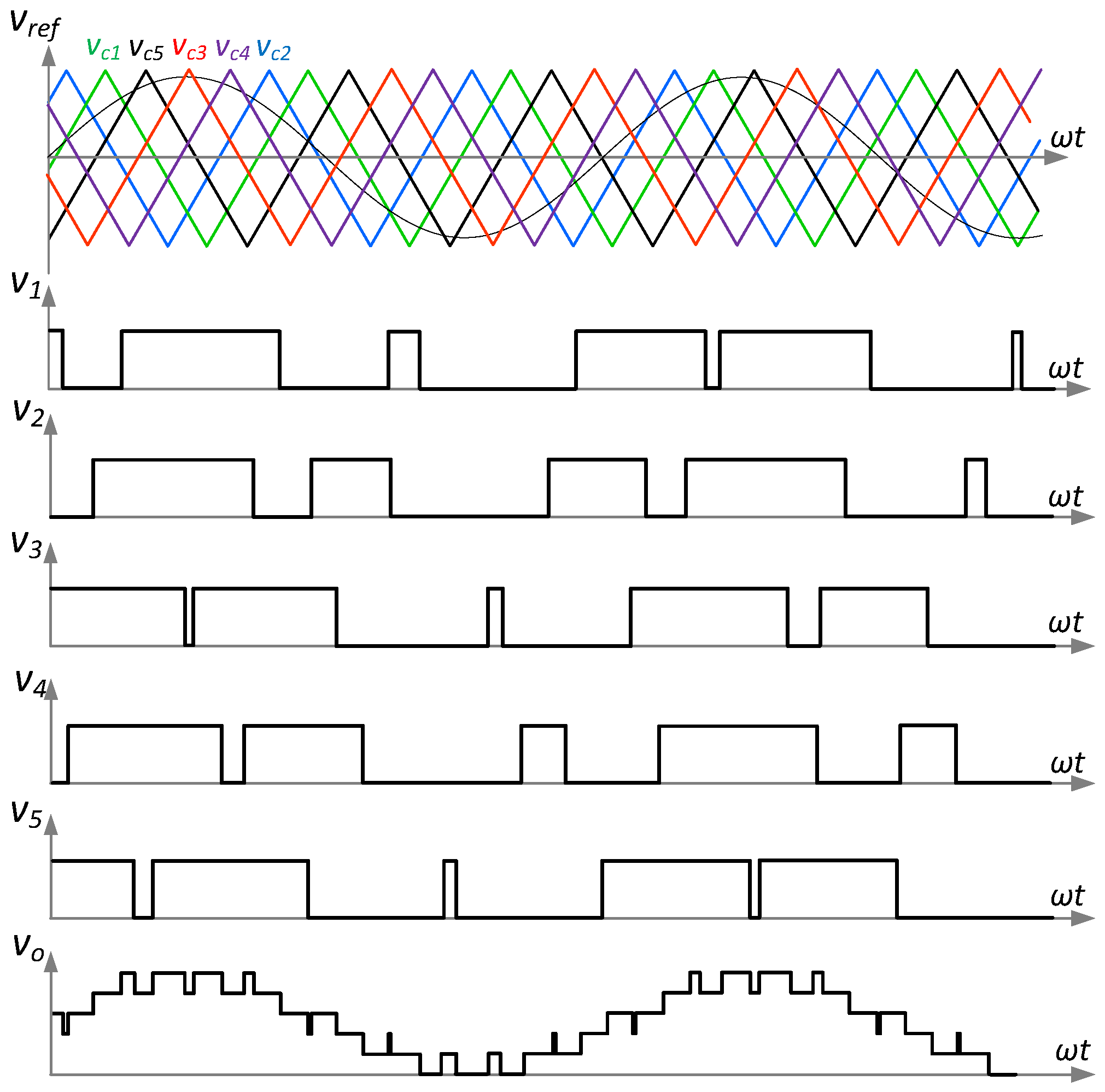
PS-SPWM is a popular multicarrier PWM technique for multilevel converters given its easy digital implementation [
12]. PS-SPWM is based on introducing a phase shift between the carrier signals of contiguous cells that produces a phase-shifted switching pattern between them and generates a stepped multilevel waveform [
4]. The main drawback of this solution is that as the number of levels of the converter increases, the phase shift between carriers become ever smaller, so that the generation of the carriers must be highly accurate.
SVM computes the switching times based on the three-phase space vector representation of the reference voltage and the inverter switching states [
4]. The reference voltage is generated as a linear combination of the switching state vectors obtaining an averaged output voltage equal to the reference over one switching period [
3]. SVM have attracted much attention because it provides significant flexibility to optimize switching waveforms with the objective of improving DC-bus voltage utilization or reducing the common-mode voltage and it is suitable for being implemented in digital signal processors [
12,
13]. Several authors have work in the development of SVM techniques for multilevel converters [
14,
15,
16,
17].
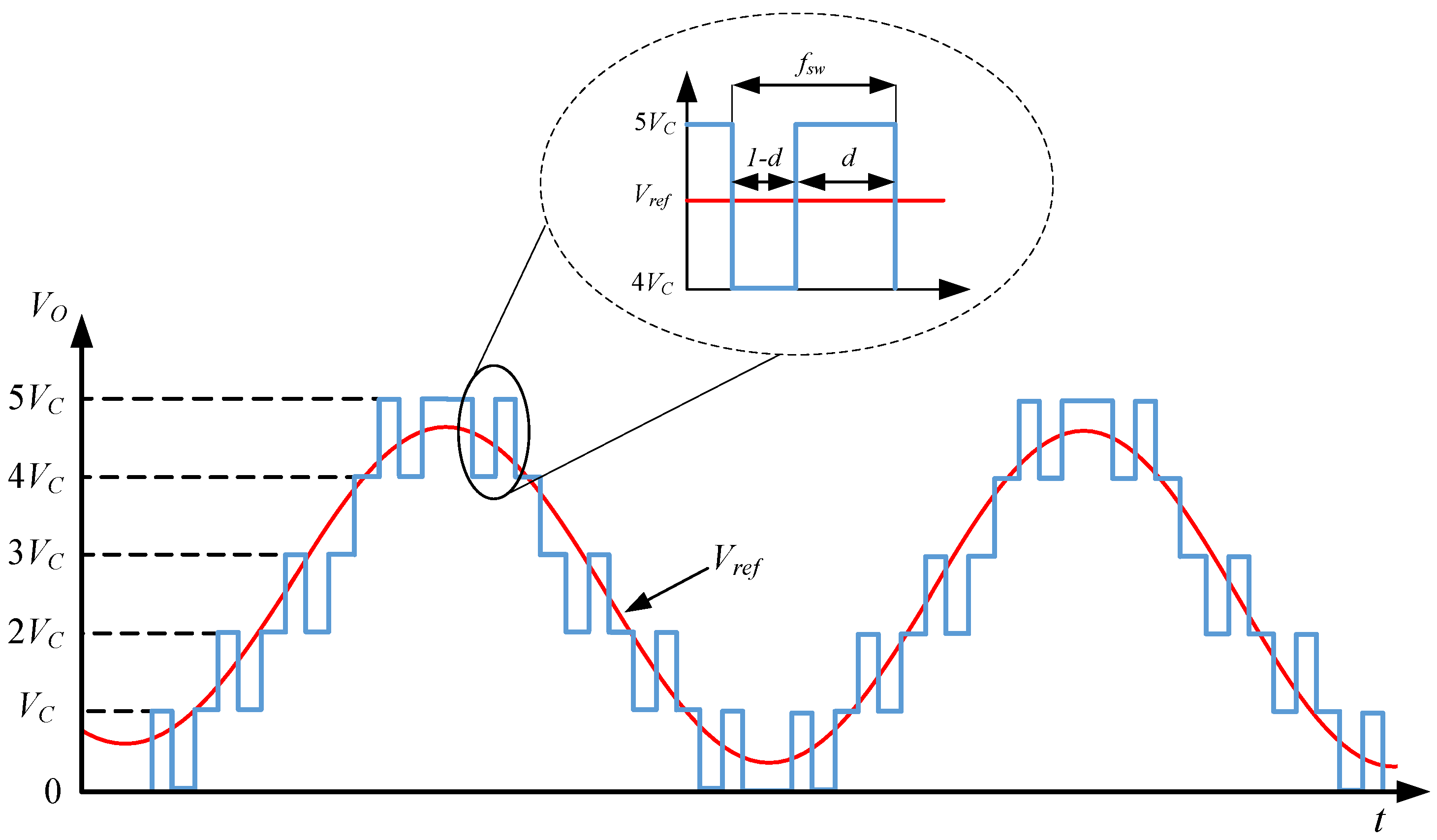
NLM is based on selecting the nearest voltage level that can be generated by the converter to the desired output voltage reference [
4]. This method avoids the use of any carrier wave, by directly computing the switching states and duty cycles for each phase of the converter. NLM brings more flexibility and easy digital implementation, even if the number of levels of the converter is large.
The article seeks to provide a set of practical criteria for the choice of a modulation method for MMCs. Despite the fact that the three mentioned modulation strategies have been studied in the scientific literature, the authors have not found an article in which the three methods are compared and, in general, there is a gap about their digital implementation for MMCs. Digital implementation is generally not described. For that purpose, firstly, the three mentioned modulation methods are compared according to their generated harmonic content; secondly, the three modulation algorithms are compared in terms of their digital implementation on a FPGA-based system. The paper is organized as follows:
Section 2 presents the MMC topology. The three modulation strategies under study are briefly described in
Section 3.
Section 4 shows the comparative study of the harmonic content generated by each modulation strategy.
Section 5 presents the implementation of the three modulation algorithms on the FPGA-based digital platform and shows the experimental results.
Section 6 concludes the paper.
2. Modular Multilevel Converter
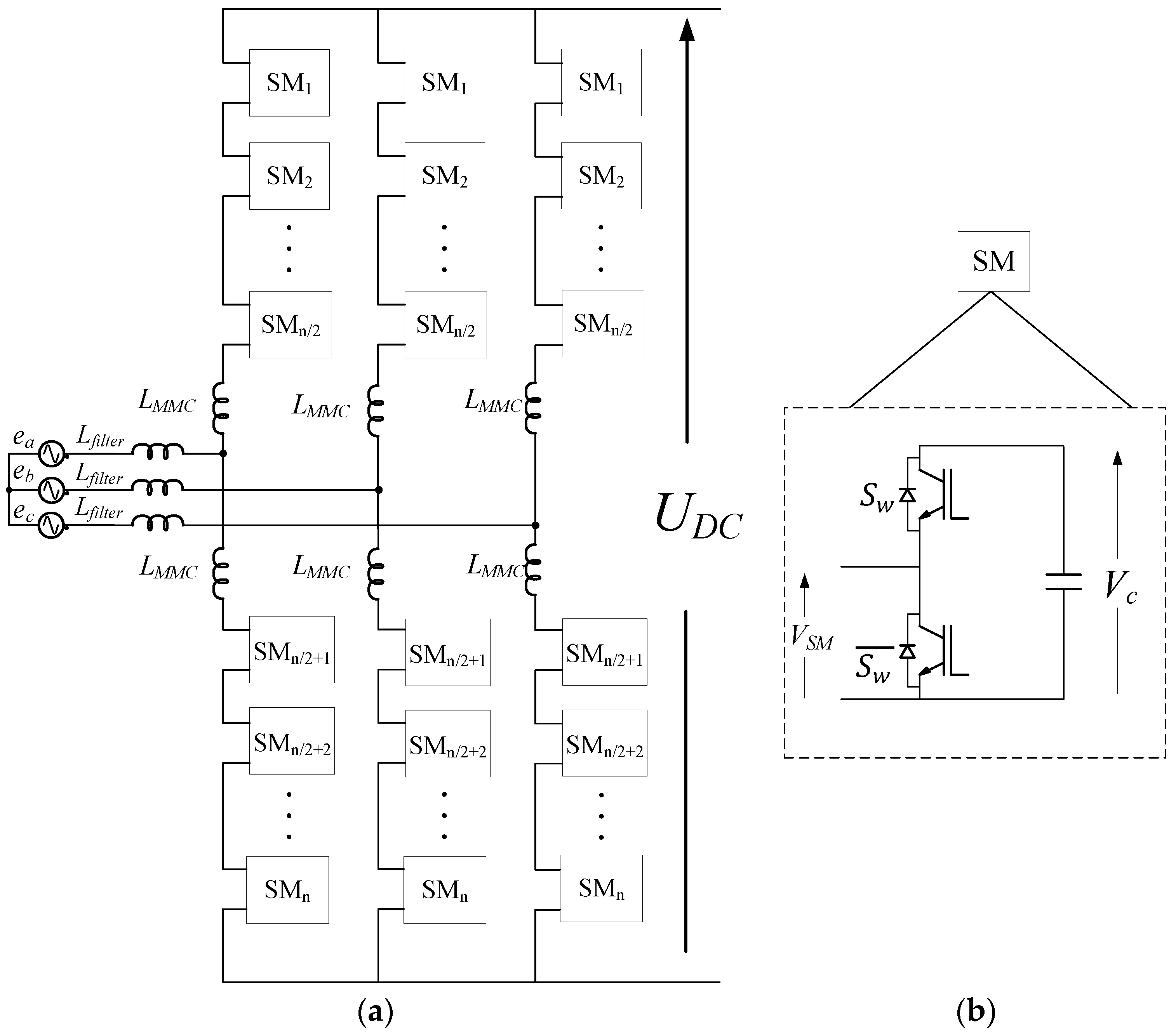
Figure 1a shows the structure of a three-phase MMC, which is composed of two arms per phase. Each arm consists of (
n/2) series-connected submodules (SMs), being
n the number of SMs per phase, and an arm inductor,
LMMC. The Direct-Current bus (DC-bus) voltage (
UDC) is equally distributed between all SMs, being the SM’s DC voltages,
Vc, equal to:
SMs of the MMC used in this article are half H-bridges, as shown in
Figure 1b. Each SM contains two switches (IGBT and reverse diode) and a DC storage capacitor. The IGBTs are managed with complementary signals,
S and
, existing two possible values of the SM’s output voltage,
VSM. When
S = 1,
VSM =
Vc. If
S = 0,
VSM = 0 V. Therefore, the converter output voltages can take
n + 1 voltage levels. Adding a new SM per arm increases in two voltage levels the possible values of the output. Half H-bridge topology is the most common SM [
5], although there are other SM topologies that provide more output levels at the price of increasing the number of components, e.g., full H-bridge, multilevel Neutral Point Clamped (NPC) or Flying Capacitors (FC) cells [
18].
4. Generated Harmonic Content
In this section, the harmonic content generated by each modulation method is analyzed and compared in order to set design criteria in advance. The harmonics content generated by each modulation strategy according to the modulation index is a key point. This study reveals which are the harmonics generated by each modulation technique and facilitates a criterion for choosing the most appropriate modulation technique according to the requirements.
Due to the fact that the modulation methods under study are quite different from each other, the order of the generated harmonics will be different among methods. In order to set a common framework and to facilitate the analysis, some variables are defined below.
The amplitude modulation index,
ma, is defined as the value of the fundamental voltage harmonic,
Vfund, divided by the value of the reference signal,
Vref:
The other variable is a frequency relationship,
rf. In the case of the PS-SPWM,
rf relates the carrier frequency,
fcr, and the frequency of the modulating signal,
fref, as:
In SVM and NLM
rf is defined as the switching frequency,
fsw, used to rotate between the three vectors in the SVM or to switch between the two voltage levels in the NLM, divided by the modulating signal frequency,
fref:
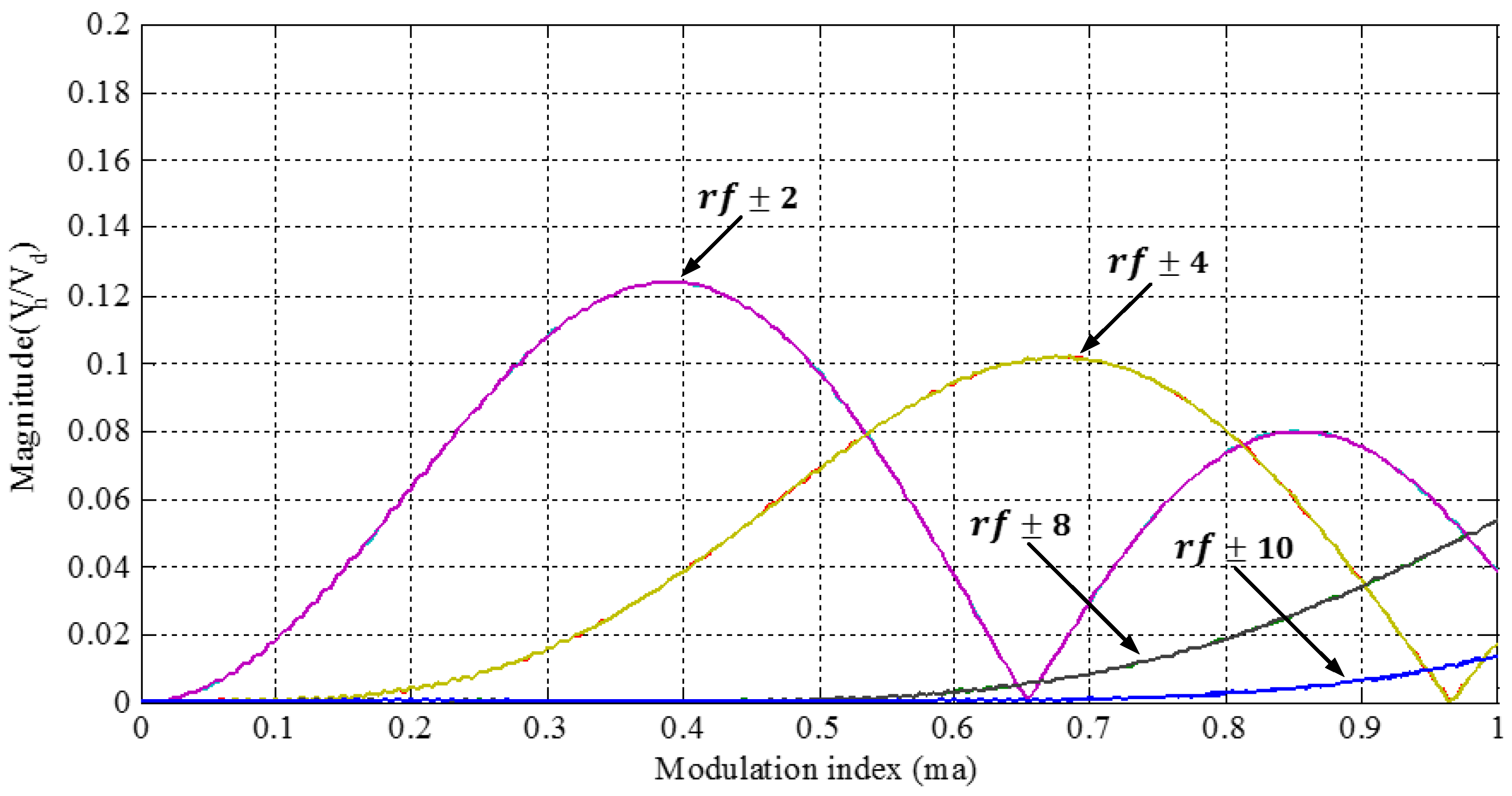
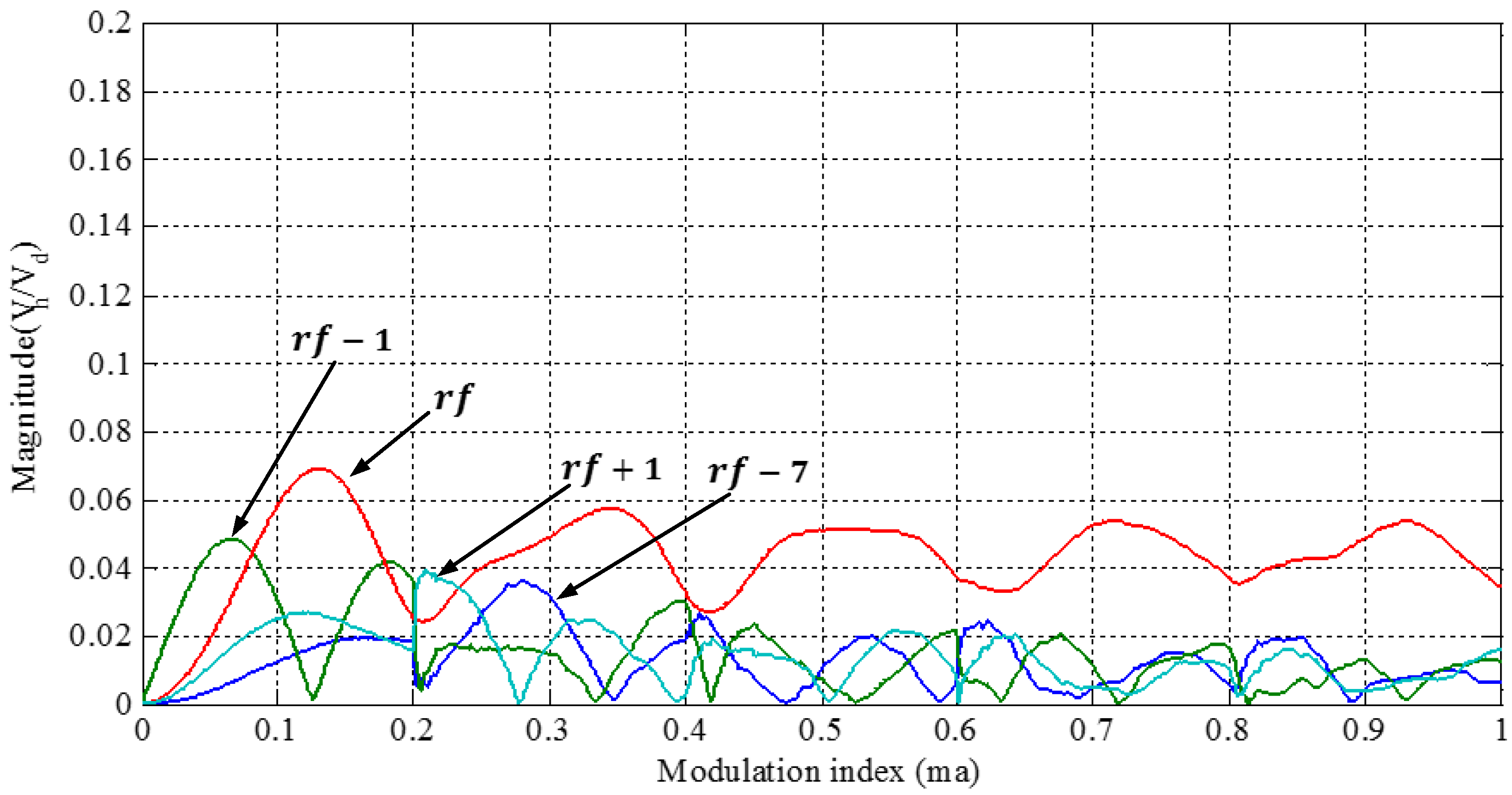
The simulation results obtained for PS-SPWM are shown in
Figure 10, which presents the harmonic distribution according to
ma. The harmonics with the highest amplitude are generated at
rf ± 2 and
rf ± 4.
In the SVM technique, the harmonic content is lower compared to PS-SPWM or NLM (see
Figure 11). Since there is a high degree of flexibility in this modulation technique, the harmonic distribution largely depends on the chosen vectors.
The results for NLM are shown in
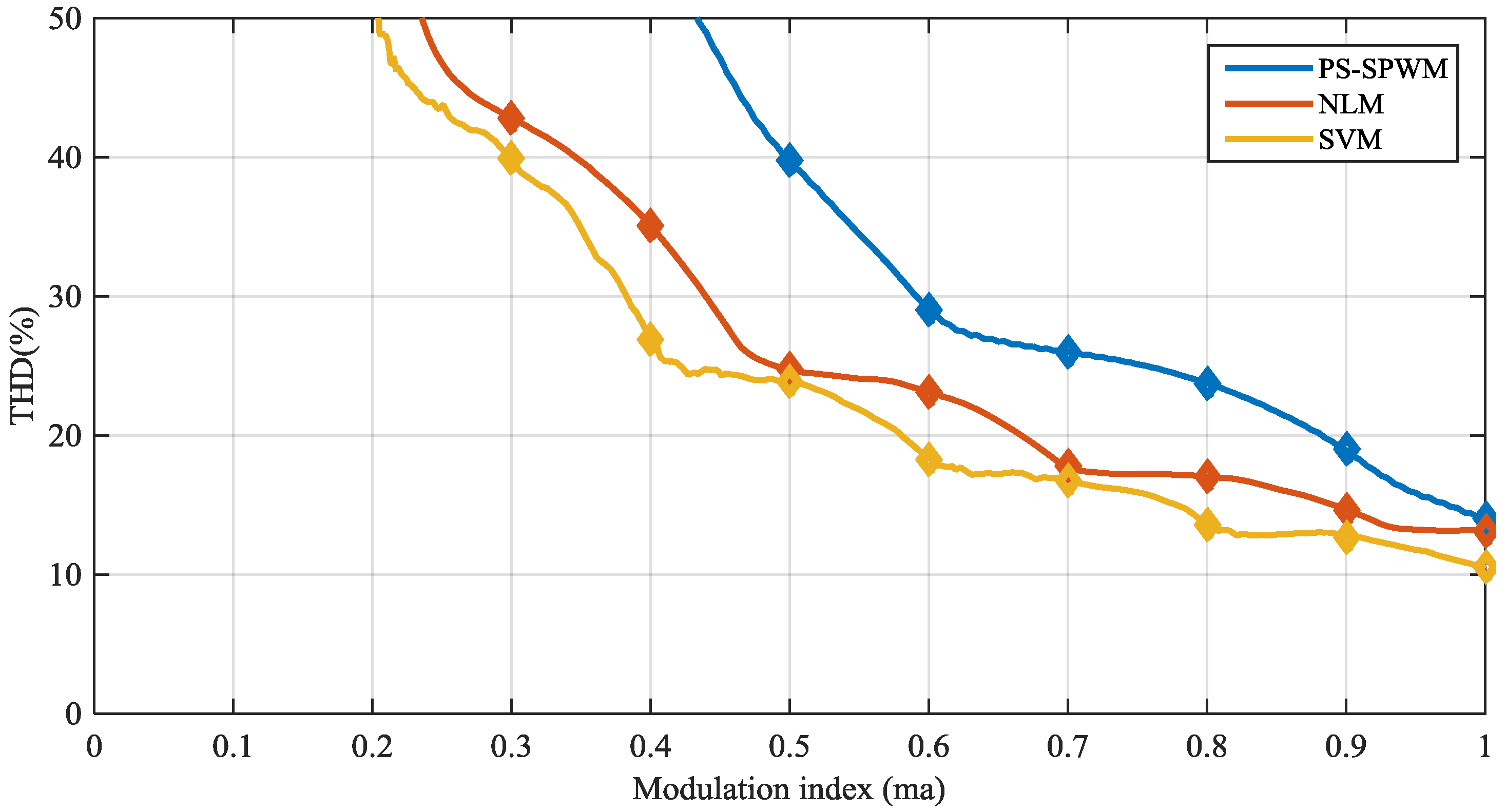
Figure 12. The harmonics in NLM method have less amplitude compared to PS-SPWM but higher than SVM. The THD obtained with each modulation is shown in
Figure 13. The figure represents the THD of the line-to-line voltage according to the modulation index. For the purpose of comparing the THD of the three modulation techniques, different frequencies for each modulation have been employed in order to have the same number of transitions per cycle. Thus, The PS-SPWM uses carrier signals at 750 Hz. The SVM and the NLM calculate the duty cycle by means of a frequency of 5.25 kHz and 3.75 kHz, respectively. The figure shows that, in the case of PS-SPWM, the THD is higher than in NLM and SVM methods. However, as
ma increases, the difference between modulation techniques is lower.
Table 1 shows a comparative analysis regarding the amount of switching transitions performed by each IGBT during one cycle of the fundamental signal (0.02 s) using the aforementioned switching frequencies. The Table shows that using the proposed implementation, PS-SPWM has the lowest number of switching transitions followed by the SVM. For the same number of output switching transitions, the results show that the NLM requires twice the number of transitions of PS-SPWM.
5. Experimental Results
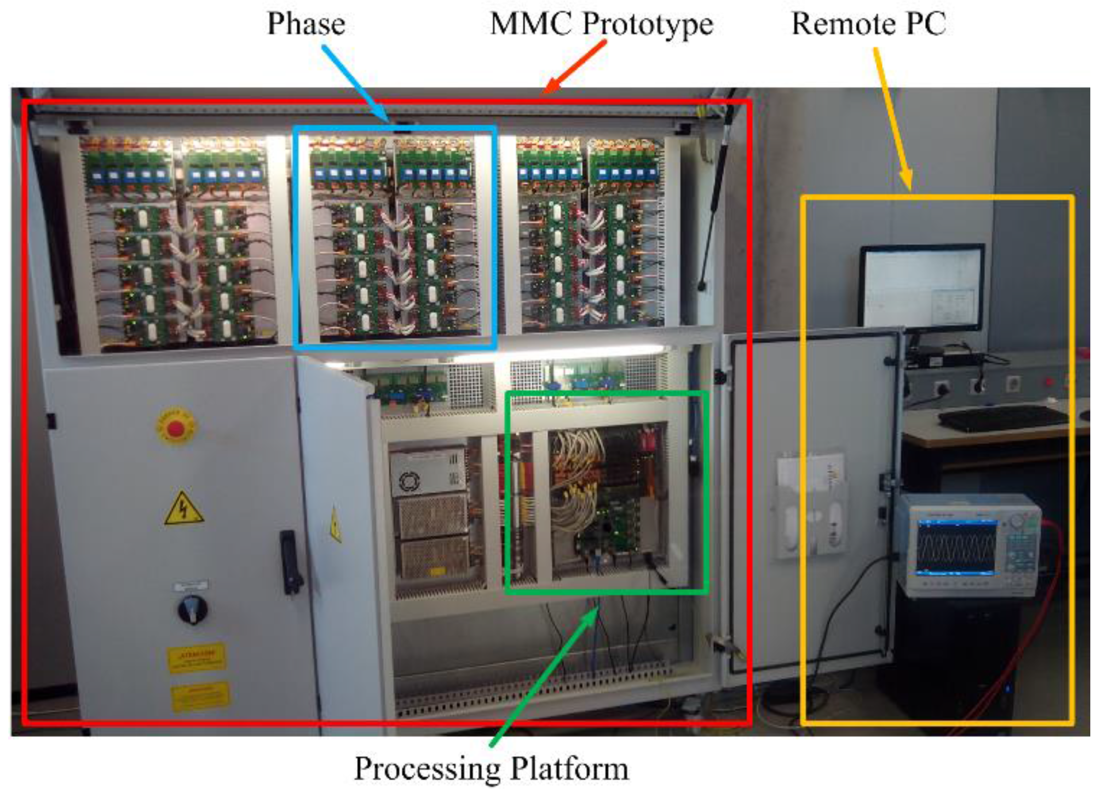
The three modulation methods have been validated and evaluated in the real six-level MMC prototype shown in
Figure 14. The main parameters of the converter are presented in
Table 2. The switching frequency of each modulation technique is the same that in
Section 4. The PS-SPWM has been implemented with carriers of 750 Hz. The SVM and the NLM calculates the duty cycle by means of a frequency of 5.25 kHz and 3.75 kHz, respectively.
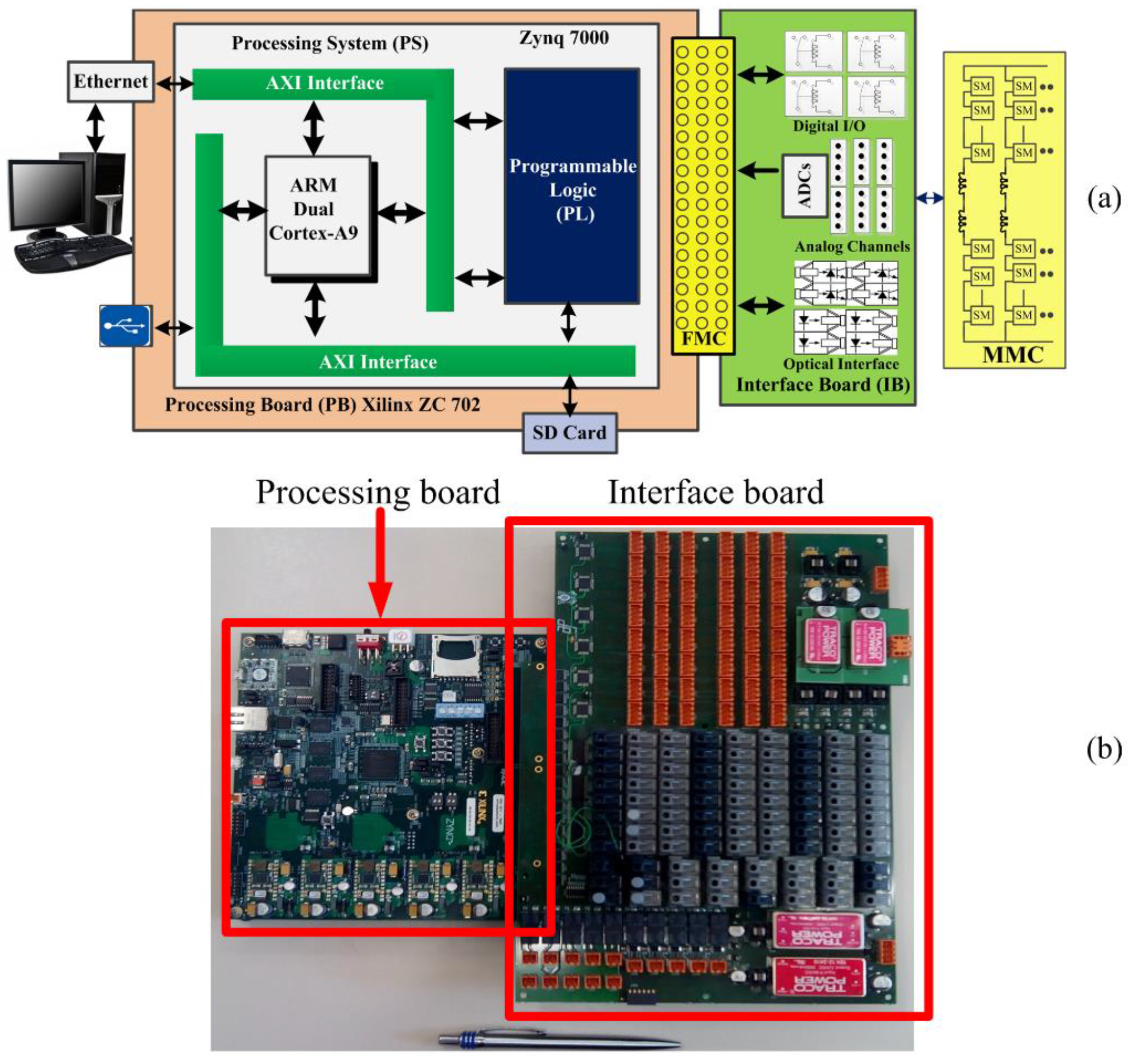
The three modulation algorithms have been implemented and tested in a control platform designed to be used in large multilevel converters. The control platform consists of two interconnected boards referred as processing board (PB) and interface board (IB).
Figure 15 presents the block diagram and a photo of this control platform.
The PB is based on the Xilinx ZC702 Evaluation board (Manufactured by Xilinx, Plano, TX, USA). The ZC702 includes a Zynq-7000 XC7Z020 SoC. This SoC integrates a dual-core ARM Cortex-A9, which constitutes the core of the processing system (PS), and programmable logic (PL) based on an Artix-7 FPGA. The purpose of the PB is twofold: firstly, it implements the bidirectional communication with the host computer through an Ethernet connection and, secondly, it executes all the converter control algorithms [
28].
The IB has been designed by the authors. It implements the interface between the power converter and the PB and carries out two main functions: (i) it adapts the signals that are exchanged with the converter, mainly sampled voltages and currents and modulation signals: (ii) it implements the acquisition system, which is used to sample the converter signals: the arm and grid currents, and the grid and SM voltages.
To the best knowledge of the authors, there are not in-depth studies about the digital implementation in a real processing platform of the three considered modulation techniques. The modulation techniques have been usually implemented in a Digital Signal Processor (DSP) due to the ease implementation [
18,
27]. However, this approach has several disadvantages such as the increased DSP processing time or a reduced accuracy due to the limited available resources. In this paper, the three modulation techniques have been implemented in a FPGA-based processing platform. Although the FPGA-based approach can increase the implementation complexity, it considerably improves accuracy and performance, meanwhile processing time is greatly reduced.
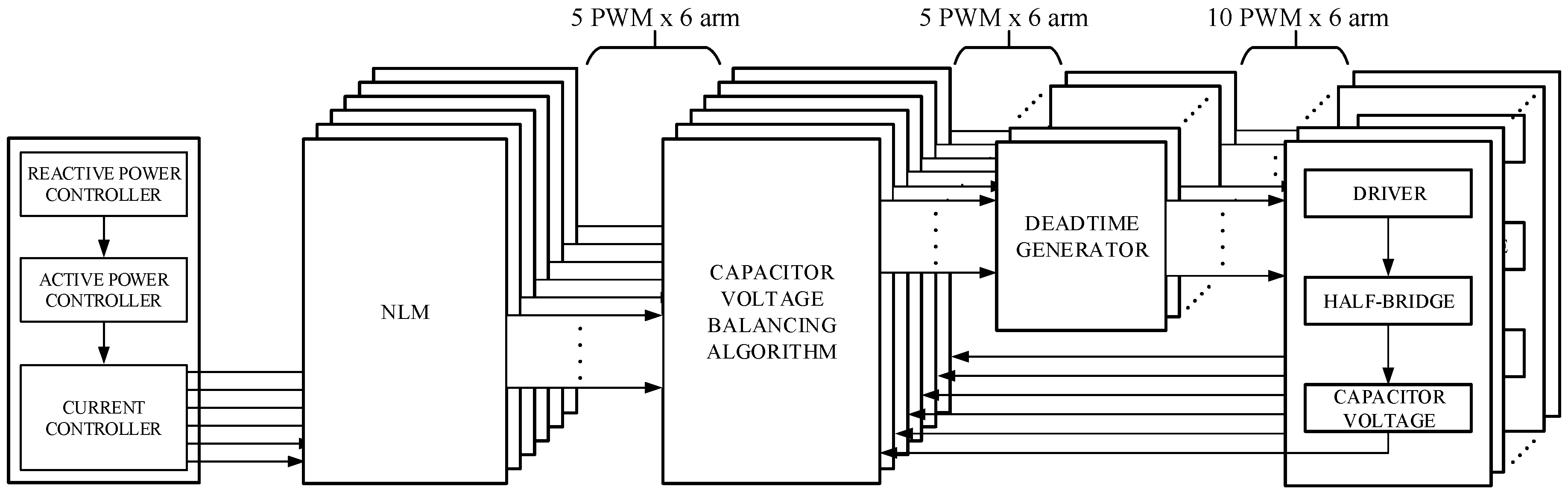
The entire modulation techniques have been implemented in the PL blocks of the PB. The available resources are 85,000 logic cells (LCs), 53,200 look-up tables (LUTs) and 106,400 flip-flops. The modulation methods have been implemented as Intellectual Property (IP) peripheral cores. These cores are connected to the AXI-bus of the FPGA, which interconnects modulation blocks and control loops. The advantage of use such cores is they can be exported to other devices without changes, reducing the development time. In addition, the three modulation techniques are simultaneously implemented and can be selected by the controller at any time. The implementation of each modulation technique is described below.
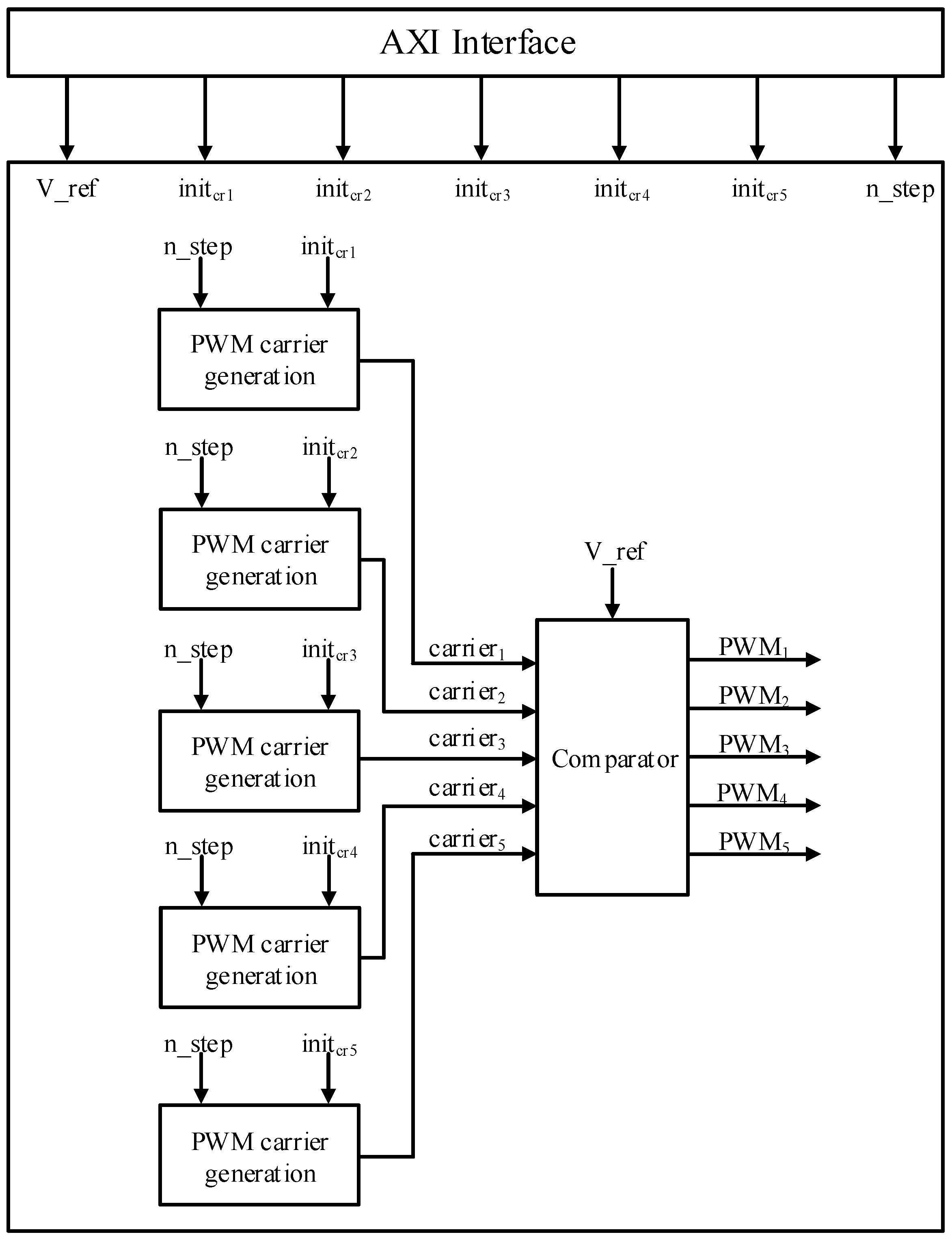
5.1. PS-SPWM
PS-SPWM requires five carrier signals to generate the gate signals of a six-level converter.
Figure 16 shows the block diagram of the per-arm implementation of the modulation algorithm. Each carrier signal is generated by the “PWM carrier generation” blocks, which allow programmable phase shift and frequency. The carrier signals are compared with the arm voltage reference and, then, five master gate signals are generated.
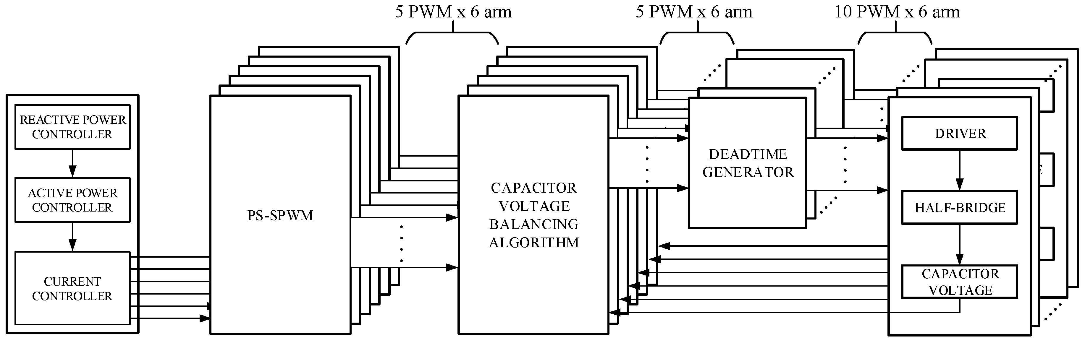
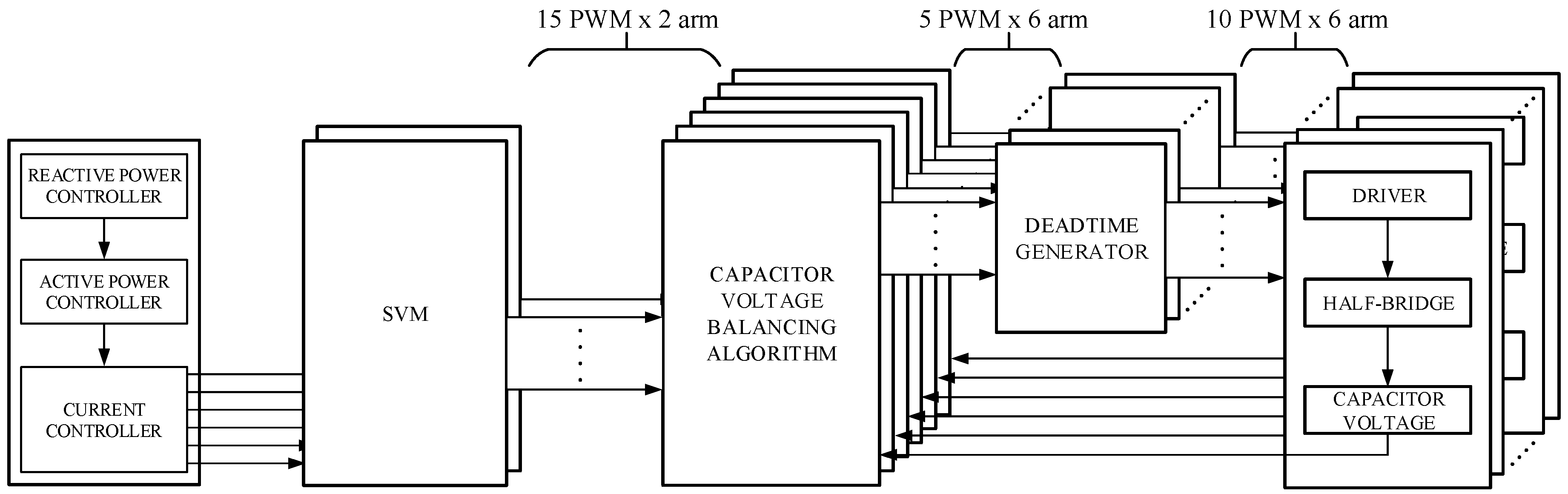
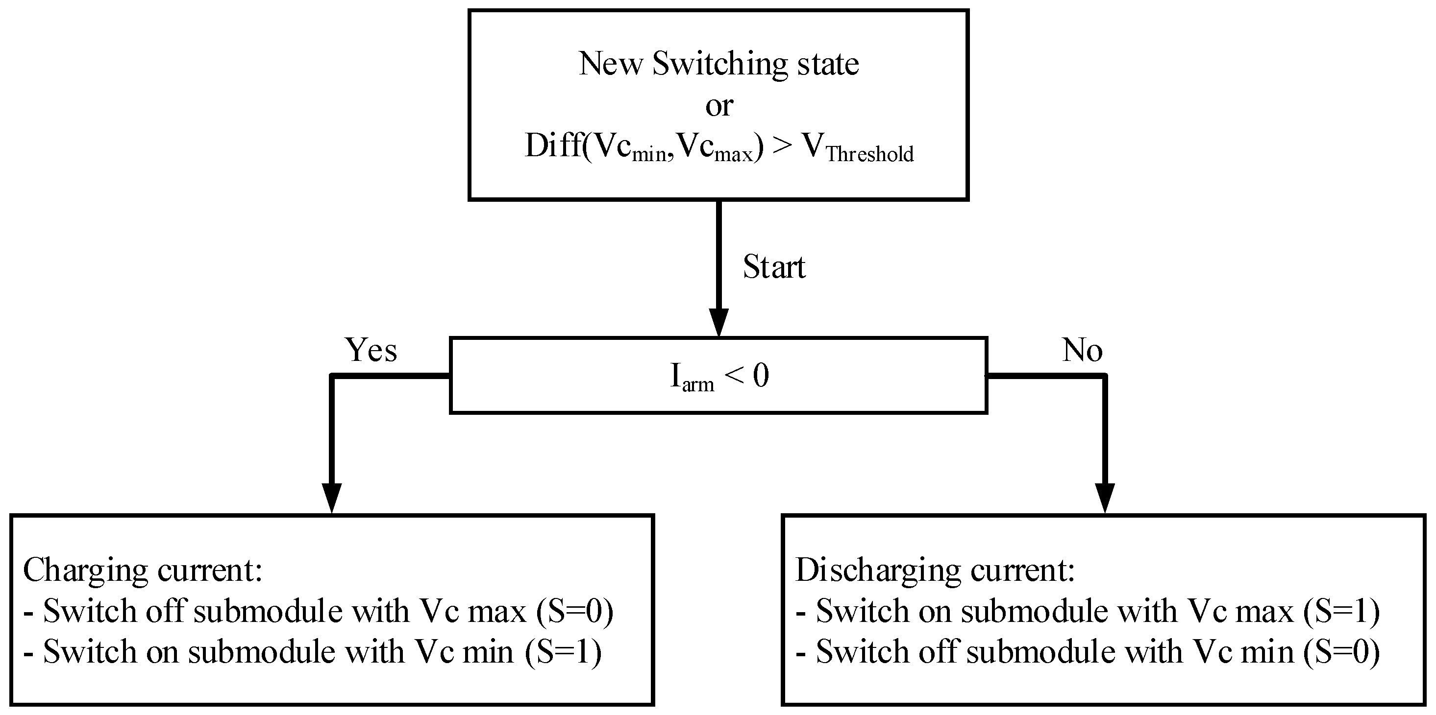
Figure 17 shows the full control diagram. Six blocks are required (one for each arm) in order to generate the PWM master signals from the six voltage references. These master signals are modified by the capacitor voltage balancing algorithm and then inverted by a dead-time controller which generates the rest of the PWM signals. Finally, the PWMs signals are applied to the SMs’ IGBTs.
Fixed-point codification is used for the reference signals and carrier signals. The amplitude of the carrier signals is fixed and normalized between −1 and 1. The frequency of the carrier signals is controlled by the step size (n_step) used to increment the signal each period. The phase shifting is controlled by the initial value of the carrier signals (initcrs).
5.2. SVM
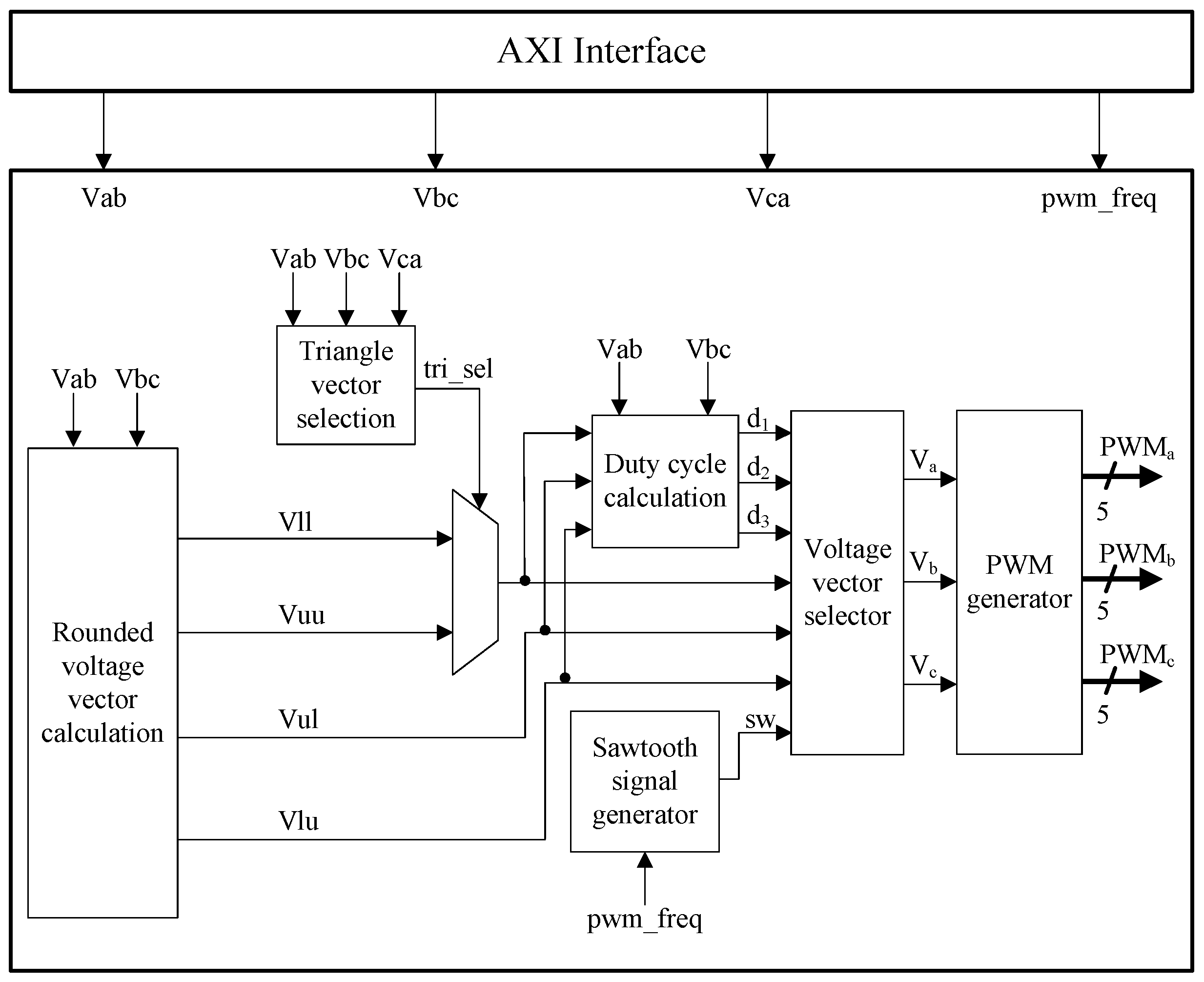
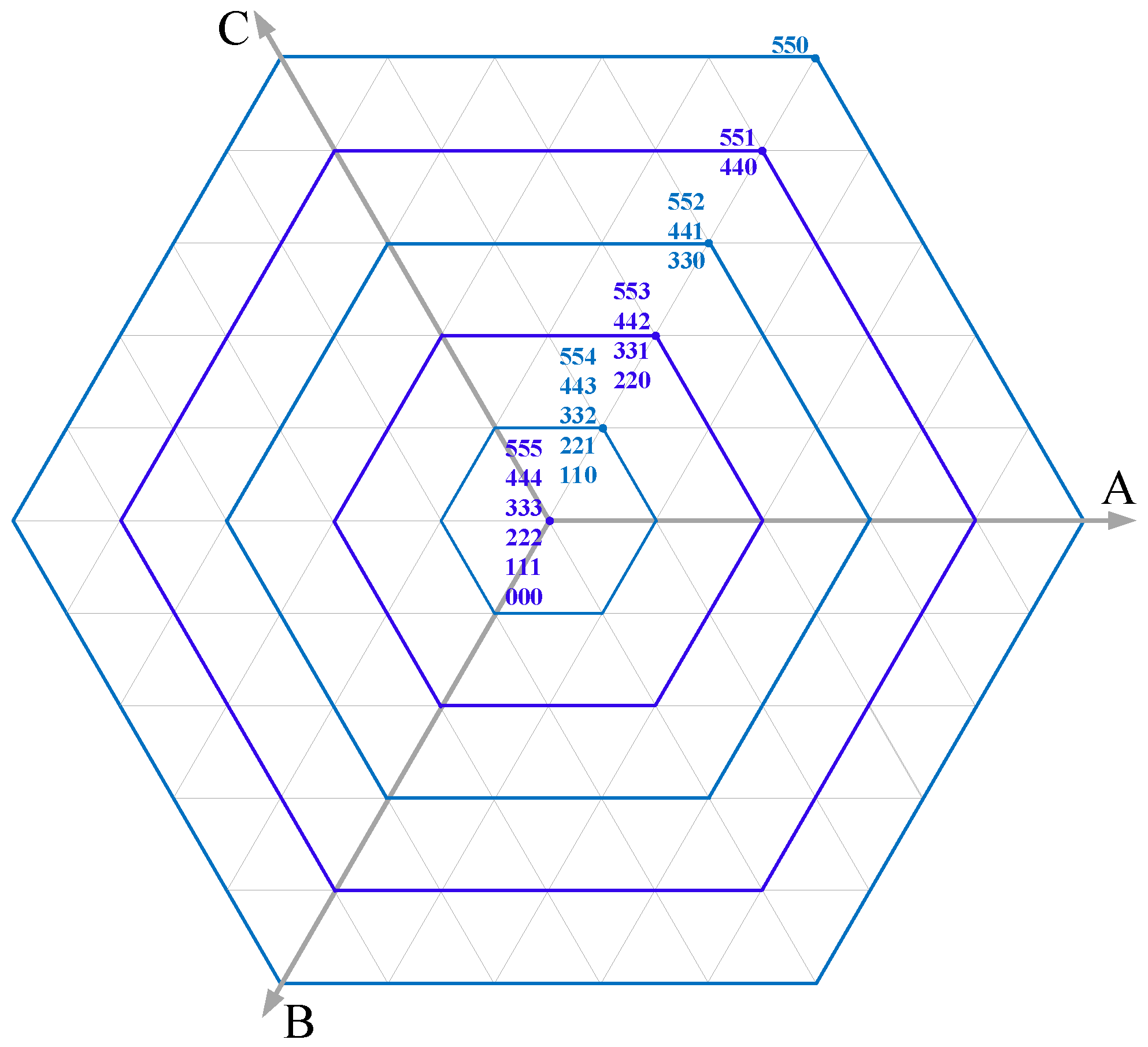
SVM presents the most complex implementation of the three modulations under study, however it provides more degrees of freedom since the voltage reference can be obtained applying multiple voltage vectors. Unlike PS-SPWM and NLM, in SVM the gate signals of the three phases must be generated in the same block.
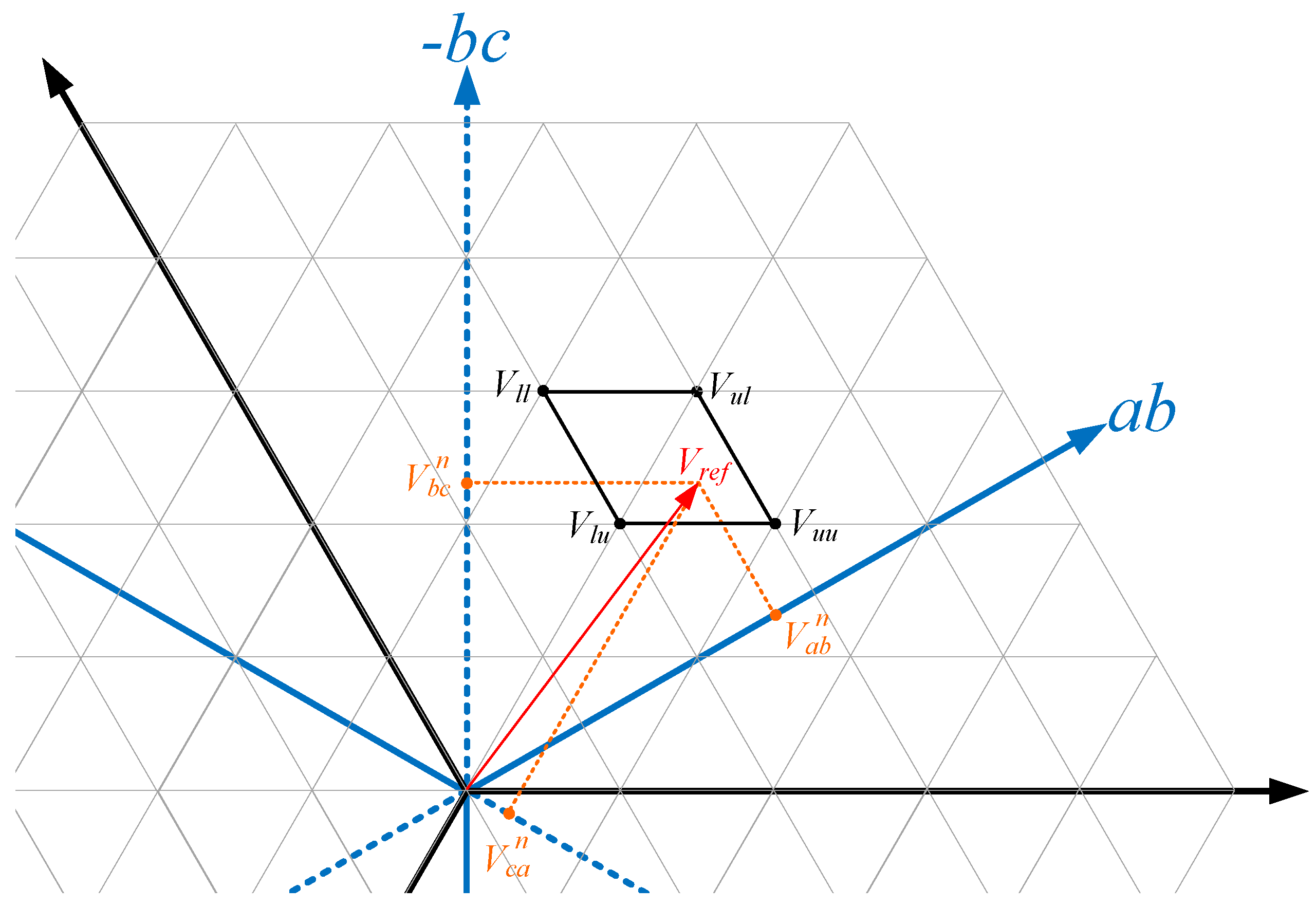
Figure 18 presents the block diagram of the implemented SVM method.
The core receives the three line voltages and, then, the block namely ‘Rounded voltage vector calculation’ calculates eight possible rounded vectors according to (3). The third vector, Vll or Vuu, is chosen from (4). The duty cycles are obtained using Vab and Vbc voltage reference signals and the three aforementioned voltage vectors by using (5) and (6).
The next step is to calculate the voltage levels of each phase to generate the corresponding output voltage level. The phase voltage is obtained from the three voltage vectors (see
Figure 4). The sawtooth signal is used to switch the output between the three voltage vectors using the duty cycles calculated above. Finally, the output voltage reference is applied to a PWM generator in order to generate the gate signals for the IGBTs. The gate signals are generated depending on the amplitude of the voltage reference and a circular array is used to rotate the switching pulses in order to distribute the switching losses.
Figure 19 shows the SVM full control diagram. Two blocks are used (one for the upper arm and one for the lower arm) in order to obtain the PWM master signals which then are introduced in the capacitor voltage balancing algorithm with the objective to balance the capacitor voltages. Finally, the remaining PWM gate signals are generated by the dead-time generator.
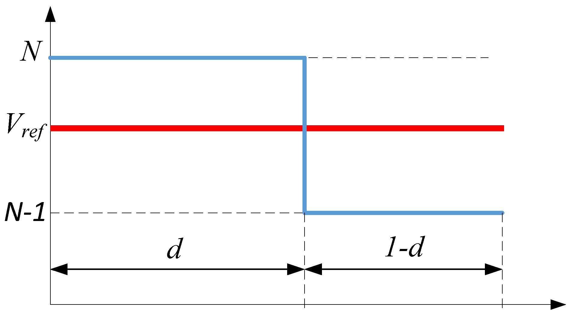
5.3. NLM
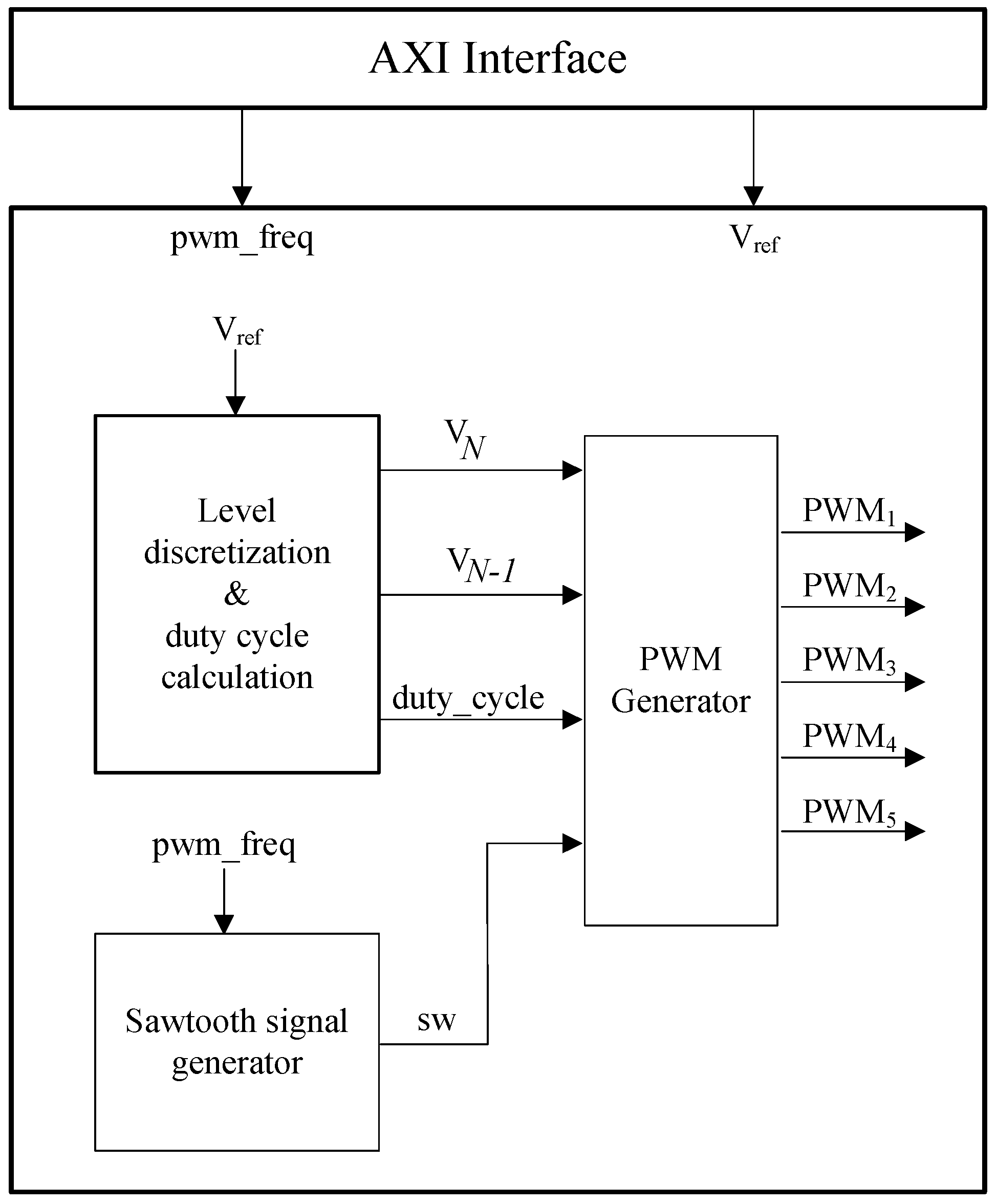
In contrast with PS-SPWM and SVM, the implementation of the NLM method is less complex as
Figure 20 demonstrates and, thus, it is a very suitable modulation method for MMC with large numbers of SMs. Only one control variable is required, the switching frequency (
pwm_freq). The core receives the voltage reference (
Vref) which is both upper rounded (
VN) and lower rounded (
VN−1) to the next nearest integer voltage level. The duty cycle is obtained from the voltage reference signal and its rounded value and (10).
A sawtooth signal with programmable frequency (
pwm_freq) is used to switch the output between two levels
VN and
VN−1. The range of the signal is (0, 1), thus, it can be directly compared with the duty cycle and therefore the right voltage level is generated. Finally, the gate signals are generated depending on the amplitude of
VN and
VN−1. As in the previous case, a circular array is also used to distribute the switching losses.
Figure 21 illustrates the NLM full control diagram. In the same way as in PS-SPWM, six blocks are necessary to generate the PWM master signals. Then, they are modified by the capacitor voltage balancing algorithm and inverted by the dead-time controller in order to obtain all the PWM signals which are then applied to the IGBTs.
5.4. Comparison of the Modulation Methods
The FPGA resources used by each modulation technique are shown in
Table 3. SVM is the modulation method that requires more resources and PS-SPWM is the algorithm that consumes fewer resources. However, the difference in the number of required resources is very small if considering the large amount of available resources in the control platform.
Although
Table 3 shows that NLM requires more resources than PS-SPWM, the resources used by this modulation technique barely increase when the number of SMs increases. Otherwise, in SPWM and SVM the resources used greatly increase when the SMs increases. In PS-SPWM due to the large number of carrier signals required and in SVM due to the complex operations required. Moreover, the resources used depend on the operation type performed (i.e., multiplication, sum, etc.) and how the code is written.
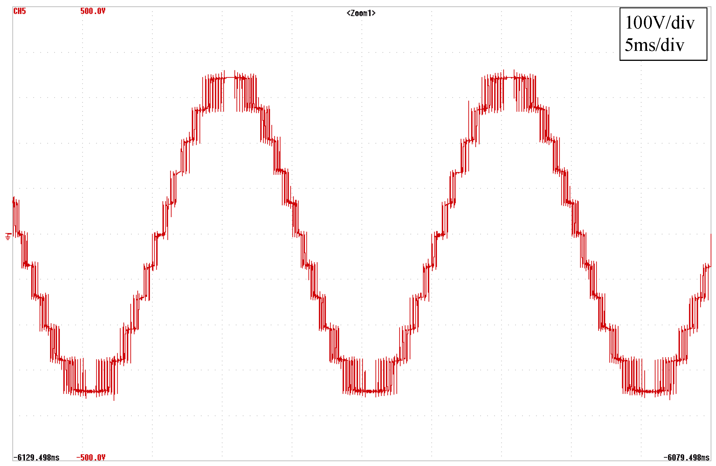
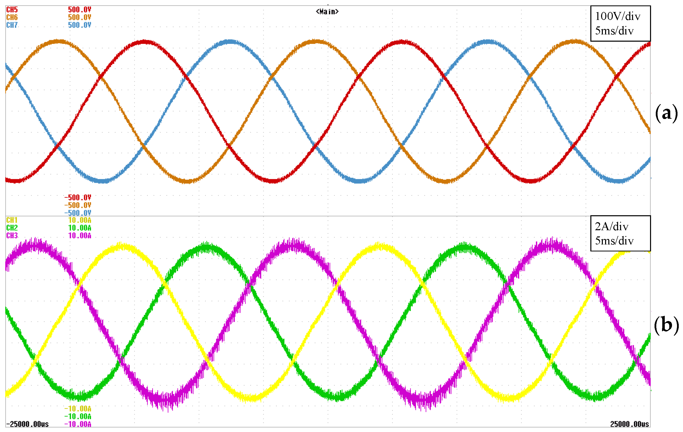
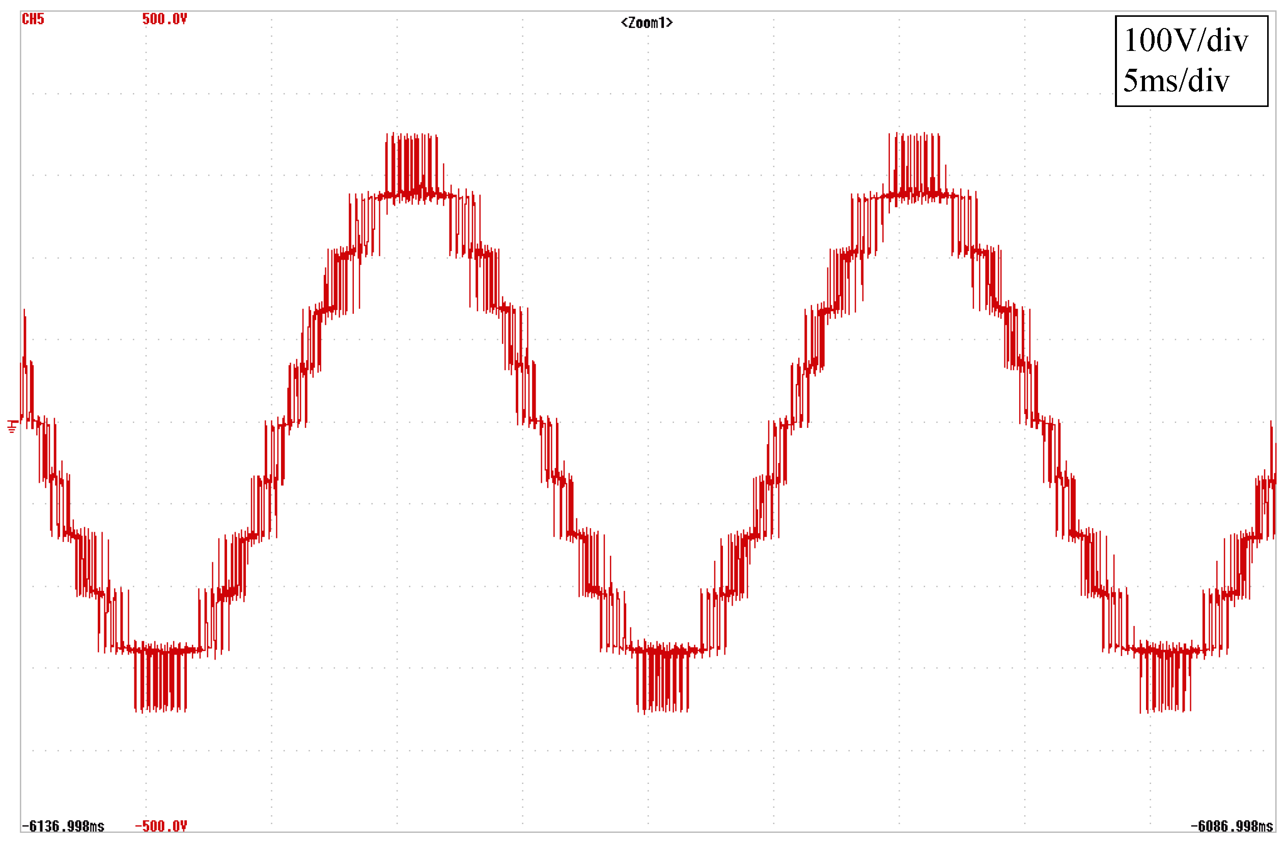
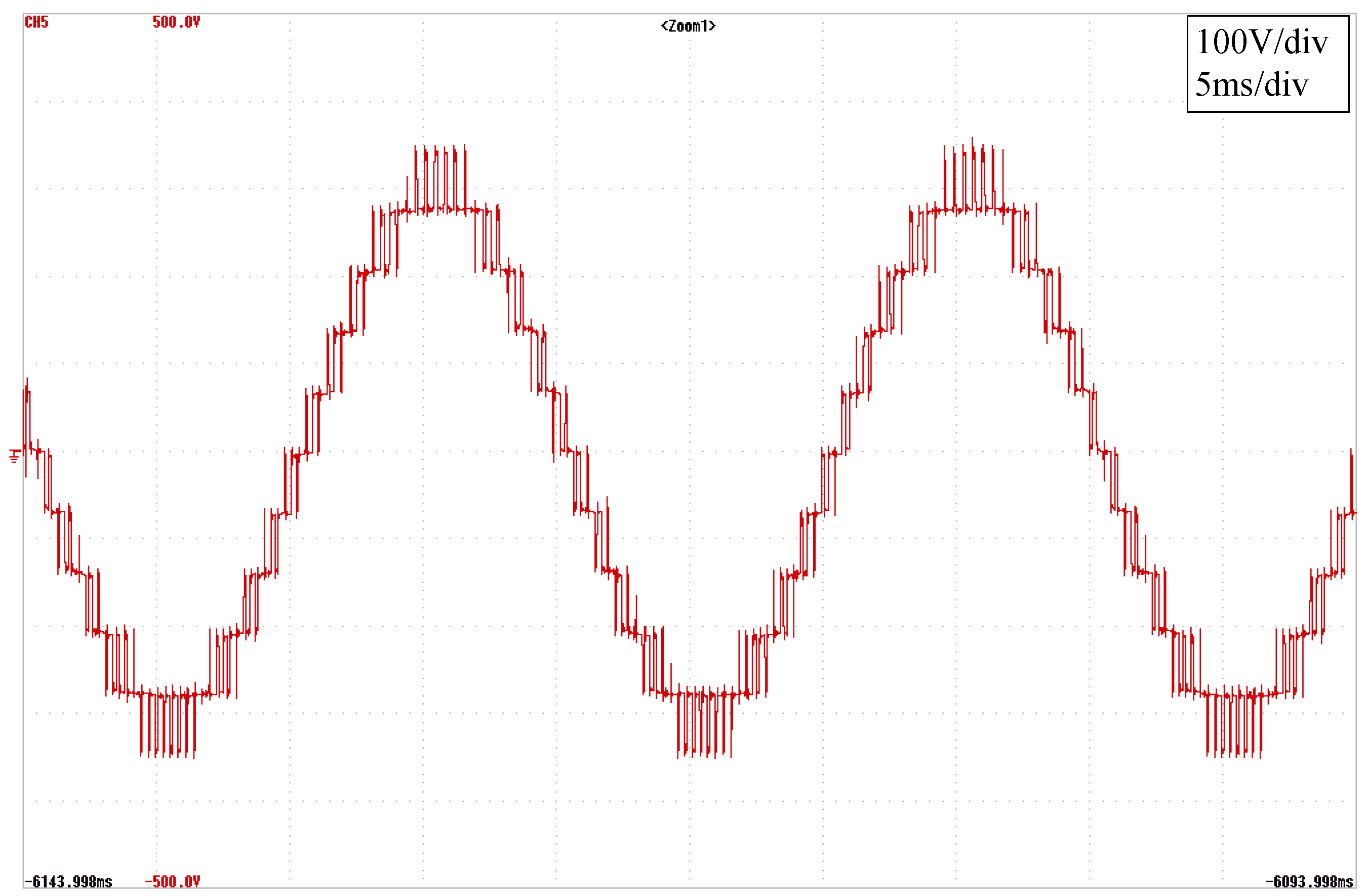
Two experimental tests have been carried out in the prototype above-mentioned. The first test consists of measuring the output voltages without any connected load. The objective of this test is to measure the output voltages without the influence of inductances that could filter the generated harmonics.
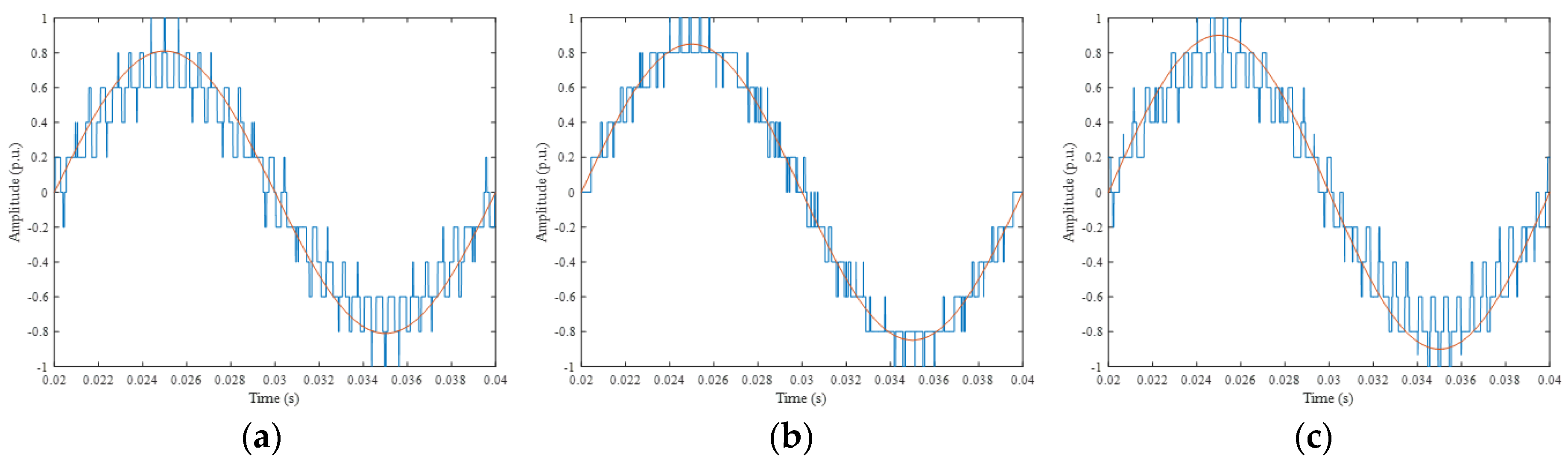
Figure 22,
Figure 23 and
Figure 24 show the line-to-line output waveform obtained using the PS-SPWM, SVM and NLM respectively. As can be seen, the three modulation techniques properly generate the waveforms.
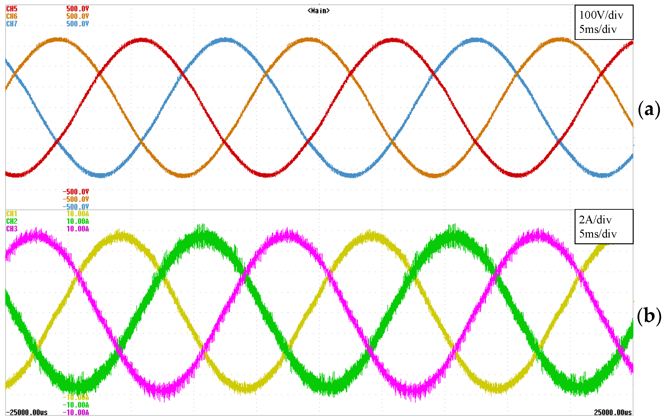
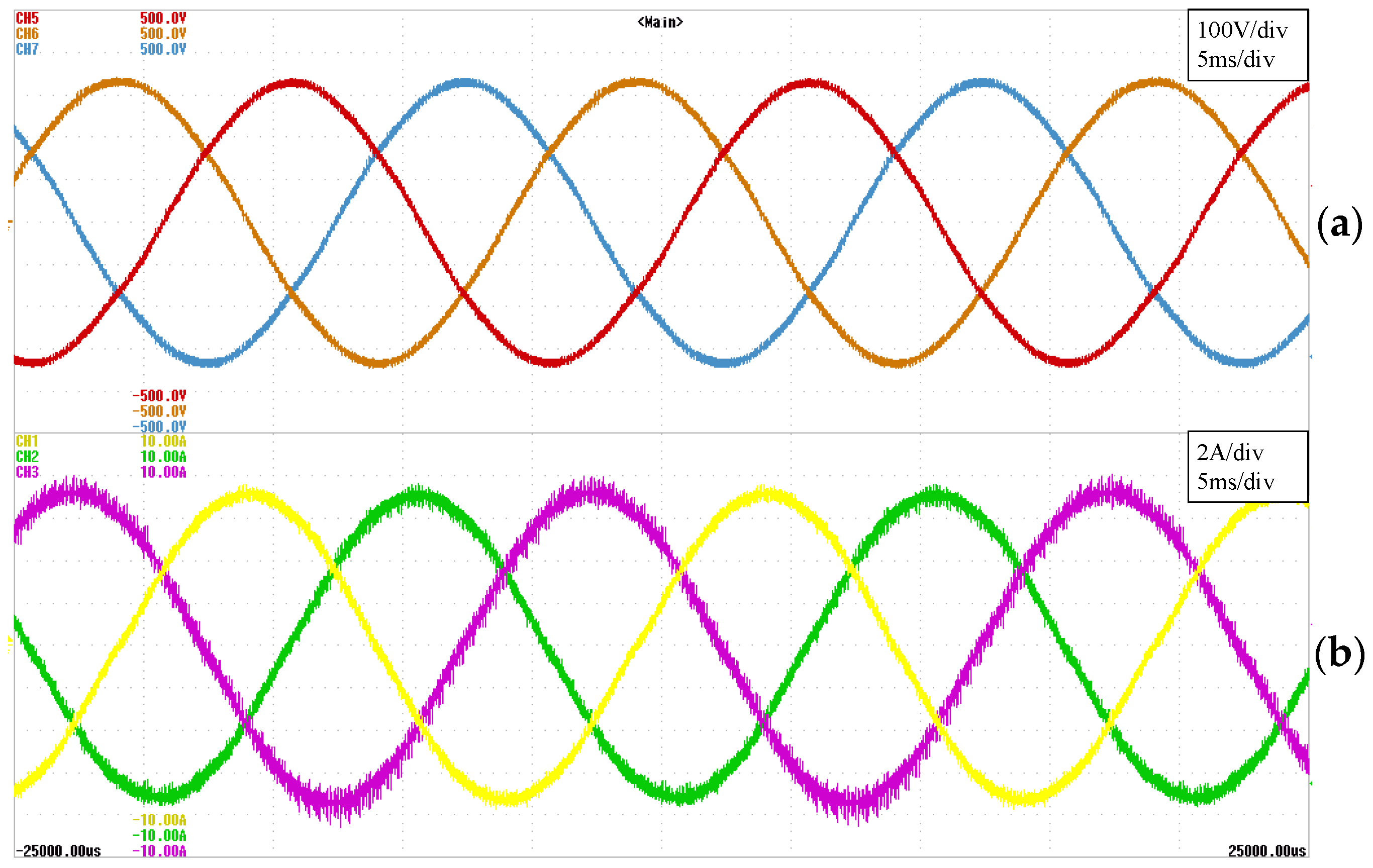
The second test consists of measuring the output currents and analyzing the harmonic content. To carry out this test, a 2 kW load is connected to the converter output.
Figure 25,
Figure 26 and
Figure 27 show the output current for PS-SPWM, SVM and NLM respectively. In addition, the output current THD for each modulation technique is shown in
Table 4. The figures show that the three modulation techniques apparently generate similar output currents. However, if the THD is analyzed, the results shown in
Table 4 reveal that PS-SPWM and SVM present a similar THD, while in the NLM case the THD is almost twice.
The experimental results validate the proposed digital implementations of the modulation strategies and corroborate the simulation results.
6. Conclusions
In this paper a comparison between different modulation techniques used in MMCs has been presented. Three modulation techniques have been studied: PS-SPWM, SVM and NLM. The paper briefly describes the three modulation strategies and presents how they are implemented in a FPGA-based digital processing platform. The proposed FPGA-based approach achieves high accuracy and reduced computational resources in comparison with a DSP implementation. In addition, the paper presents a comparative study about the harmonic content generated by each modulation technique. The results show that each modulation technique generates different harmonic content, thus, depending on the application, there will be a modulation technique more suitable than others. In MMCs with large number of SMs, the NLM is the most suitable modulation technique due to the flexibility and the facility to scale followed by the SVM which also provides reasonable flexibility. In the case of MMCs with low number of SMs, the SPWM is the best solution due to it is usually implemented in the microcontrollers designed to control power converters. Finally, the proposed implementations have been experimentally evaluated and validated in a real six-level MMC.


