Article

Optimization of Electrochemically Deposited Highly Doped ZnO Bilayers on Ga-Rich Chalcopyrite Selenide for Cost-Effective Photovoltaic Device Technology

by
Dimitra N. Papadimitriou
1,*,
Georgios Roupakas
1,
Georgios G. Roumeliotis
1,
Patrick Vogt
2 and
Tristan Köhler
3
1
National Technical University of Athens, Heroon Polytechniou 9, GR-15780 Athens, Greece
2
Technische Universität Berlin, Institut für Festkörperphysik, Hardenbergstr. 36, DE-10623 Berlin, Germany
3
Helmholtz Zentrum Berlin für Materialien und Energie, Institut für Heterogene Materialsysteme, Hahn-Meitner-Platz 1, DE-14109 Berlin, Germany
*
Author to whom correspondence should be addressed.
Energies 2016, 9(11), 951; https://doi.org/10.3390/en9110951
Submission received: 30 August 2016 / Revised: 1 November 2016 / Accepted: 1 November 2016 / Published: 15 November 2016
(This article belongs to the Special Issue Nano-Structured Solar Cells)

Abstract

:
High quality polycrystalline bilayers of aluminium doped ZnO (Al:ZnO) were successively electrodeposited in the form of columnar structures preferentially oriented along the ( 10 1 ¯ 1 ) crystallographic direction from aqueous solution of zinc nitrate (Zn(NO3)2) at negative electrochemical potential of EC = (−0.8)–(−1.2) V and moderate temperature of 80 °C on gallium rich (30% Ga) chalcopyrite selenide Cu(In,Ga)Se2 (CIGS) with chemically deposited ZnSe buffer (ZnSe/Cu(In,Ga)Se2/Mo/glass). The aluminium doped ZnO layer properties have initially been probed by deposition of Al:ZnO/i-ZnO bilayers directly on Mo/glass substrates. The band-gap energy of the Al:ZnO/i-ZnO reference layers was found to vary from 3.2 to 3.7 eV by varying the AlCl3 solute dopant concentration from 1 to 20 mM. The electrical resistivity of indium-pellet contacted highly doped Al:ZnO sheet of In/Al:ZnO/i-ZnO/Mo/glass reference samples was of the order ρ ~10−5 Ω·cm; the respective carrier concentration of the order 1022 cm−3 is commensurate with that of sputtered Al:ZnO layers. For crystal quality optimization of the bilayers by maintenance of the volatile selenium content of the chalcopyrite, they were subjected to 2-step annealing under successive temperature raise and N2 flux regulation. The hydrostatic compressive strain due to Al3+ incorporation in the ZnO lattice of bilayers processed successively with 5 and 12 mM AlCl3 dopant was εh = −0.046 and the respective stress σh = −20 GPa. The surface reflectivity of maximum 5% over the scanned region of 180–900 nm and the (optical) band gap of Eg = 3.67 eV were indicative of the high optical quality of the electrochemically deposited (ECD) Al:ZnO bilayers.

1. Introduction

Photovoltaics as a widely implemented, renewable-energy conversion technology available today has the capabilities to evolve into a major racer for industrial mass production and capital market provider by conquering occasional drawbacks. All mature technologies based either on silicon or on thin film chalcogenides (CIGS or CdTe) aim to develop large area processing at low module production costs by maintaining conversion efficiencies. Thin film device technologies actually signify the onset of cost-competitive solar technologies due to reduced material costs. Junctions based on vacuum evaporated chalcopyrite absorbers have in the past [1,2,3] and recently [4] demonstrated high conversion efficiencies. However, the production of thin film solar cells typically relies on capital expenditure intense vacuum techniques and high temperature processes, both increasing the manufacturing costs. It is thus generally recognized that a significant reduction of the production costs could be achieved, if processing technologies operating under high vacuum conditions, such as co-evaporation or sputtering, could be replaced by less expensive non-vacuum deposition techniques such as for example screen-printing and electrodeposition. Solution-processed organic and inorganic semiconductors offer a promising pathway towards low-cost mass production of solar cells.
Electrodeposition already has a major impact in the manufacture of large area metallic protective coatings using roll-to-roll processes with m/min line-speed and μm/min deposition rates. A technique with these yields would be extremely well adapted to the large-dimensioned photovoltaic industry for mass production of solar modules. However, its extension to the preparation of efficient semiconductor absorber layers remains an open challenge. Semiconductor properties are by far more difficult to control than metallic properties since they involve the activation of minority carriers at the ppm level, which is much more difficult to achieve by wet or semi-dry processing than by using ordinary dry processes under high vacuum conditions [5,6].
Spraying techniques can provide thicker coatings (μm-mm range, depending on the process and feedstock) over a large area at higher deposition rates as compared to other coating processes such as electroplating, physical and chemical vapor deposition. Important issues involved in conventional spraying to ensure suitability for high technologies and infer the future potential of novel spray processing are the use of extended feedstock: gases, liquids, and various-sized powders. Numerous industries, in recognition of the versatility and cost-efficiency of thermal and plasma sprays have introduced these technologies in their manufacturing environment. Plasma spraying as an affordable and effective thin film and coating technology [7,8] is attracting global attention in materials engineering. Recent challenges aim at a development of a co-deposition process of droplets and vapors, namely, comprehensive plasma spraying.
Printing techniques include very promising methods based on ink precursor routes that use both molecular precursor inks and monodispersed nanoparticle inks [9]. A critical requirement for using inkjet printing is to develop a suitable ink in terms of viscosity and stability that will lead to compact and homogeneous films. Hybrid inks are thus interesting from the perspective of combining the advantages of particulate-based and molecular-based precursor solutions. In fact, hybrid inks of nanoparticles mixed into a precursor are being probed: the precursor solution can act as a medium to provide effective binding between nanoparticles. The particles can act as nucleation sites to promote grain growth and film densification. Moreover, inkjet printing allows direct patterning without the requirements of any mask and can also be easily adapted to a roll-to-roll process, which is suitable for large-scale production. In this context, drop-on-demand (DOD) inkjet printing is a promising approach allowing on-demand patterning of materials with negligible materials waste. Hence, significant reduction of raw materials cost can be achieved. Solution processing of multicomponent chalcopyrite (CuInS2 (CIS), CuInSe2, Cu(In,Ga)Se2 (CIGS), Cu(In,Ga)(Se,S)2) and kesterite (Cu2ZnSnS4, Cu2ZnSnSe4 (CZTS)) thin film solar cells (TFSCs) is considered a promising alternative fabrication route to the conventional high cost vacuum techniques [10,11,12]. Less than 20 μL ink is needed to build up a micrometer kesterite (CZTSSe) thin film absorber on a large area (75 × 75 mm2) Mo coated substrate [12].
For the development of high-efficiency heterojunction solar cells based on thin-film semiconductors, an approach has been introduced based on the growth of thin passive surface layers on top of an active layer [13]. These are principally layers of higher-band gap semiconductors. The increase in the effective barrier height occurs due to the band gap discontinuity at the interface between active layer and surface layers. In a homojunction solar cell, a significant part of photogeneration takes place close to the surface of the emitter and this requires careful design of the emitter depth and doping level, and good surface passivation. In contrast to the homojunction device, in a window-absorber heterojunction cell, the generation maximum is shifted to the p-n junction where the electrical field is at its maximum and contributes to the collection of photogenerated carriers. Due to the high band gap window, only a few carriers are generated close to the surface and the influence of surface recombination can thus be neglected. Recent progresses in materials research and applications inclusive structural, morphological, optical, and electronic properties of transparent conducting ZnO used as transparent electrode in thin-film solar cells are reviewed in [14]. The deposition technologies involved are exclusively in-vacuum processes such as chemical vapor deposition (CVD), pulsed laser deposition (PLD), sputtering, and sputtering combined with texture-etching. Alternatives for replacement of the traditional CdS buffer of chalcopyrite semiconductor based heterojunction solar cells are reviewed in [15]: an overview of various thin films (ZnS, ZnSe, ZnO, (Zn,Mg)O, In(OH)3, In2S3, In2Se3, InZnSex, SnO2, and SnS2) deposited on differently processed chalcopyrite absorbers with deposition methods embracing both, in-vacuum and liquid-phase processes (chemical bath deposition (CBD), atomic layer deposition (ALD), metal organic chemical vapor deposition (MOCVD), ion layer gas reaction (ILGAR), sputtering, thermal evaporation, and electrochemical deposition (ECD)), and the achieved solar cell efficiencies is given there. Several processes have demonstrated efficiencies comparable with the CBD CdS standard. Thin films acting as buffers of CIGS TFSCs are thus already separately being processed by low cost chemical, electrochemical, and printing techniques [15,16,17,18].
Overall application of inexpensive, non-vacuum chemical (CBD) and electrochemical deposition (ECD) techniques targeted for processing the absorber-, buffer-, and window-layer of CIS/CIGS TFSCs to overcome current process incompatibilities mainly resulting from the simultaneous use of moderate temperature non-vacuum (50–70 °C) and high temperature (500–700 °C) vacuum processes was reported in one of our previous publications [19]. Low cost ECD processing of ternary CuInSe2 and quaternary Cu(In,Ga)Se2 chalcopyrite selenides with crystal quality similar to that of PVD grown films was achieved by as few as possible process steps thus skipping selenization at elevated temperatures [19,20]. Chalcopyrite phase formation was confirmed already in as-deposited films. The film quality was further improved by subsequent annealing at 300 °C, for 2 h, in N2 ambient. ZnSe buffer- and ZnO window-layers were processed by CBD and ECD techniques, respectively [19]. By successive integration of low cost ECD ZnO/CBD ZnSe window and buffer components in CIS/CIGS solar cells with absorbers grown by standard vacuum techniques, the respective p-n junctions exhibited I-V characteristics competing with monocrystalline silicon (c-Si) I-V. The properties of ECD processed n-ZnO/i-ZnO bilayers were extensively investigated with respect to conducting and semi-conducting substrate influences, layer thickness, dopant type and dopant concentration, strain accumulation, and electrical resistivity, in a more recent publication [21]. The properties of ZnO nanorod arrays grown by ECD and probed to serve as antireflective coating (ARC) of CIGS solar cells have also been thoroughly analyzed [21,22]. In the present work, optimization of structural, optical, and electrical properties of Al:ZnO bilayers deposited by ECD on ZnSe/CIGS/Mo/glass is attempted aiming to minimization of strain and maximization of carrier mobility in the respective solar structures through optimization of the various ECD process parameters towards up-scale to industrial processes.
In vacuum grown Cu(In,Ga)Se2 with excess of gallium has intentionally been chosen, since with increasing Ga content, the band gap of CIGS and the stability domain of the chalcopyrite phase increase significantly with respect to ordered defect compounds, while the acceptor transition levels are shallower in CGS than in CIS and the GaCu donor level in CGS is much deeper than the InCu donor level in CIS [23]. According to literature referred in [24], the best efficiencies of CIS/CIGS TFSCs are reached using sulfides with 10% and selenides with 25%–30% Ga content. For larger Ga-fractions, the photovoltage saturates leading to a decrease of conversion efficiencies [25]. The absorption coefficients of the quaternary CuIn1−xGaxSe2 alloys with [Ga]/([In] + [Ga]) ~0.30 may become as high as 6 × 105 cm−1, at optical energies, and the band-gap is widened-up towards the optimum Eg = 1.5 eV for solar energy conversion. With 30% gallium substituting indium, the band-gap energy is up-shifted to 1.15 eV [26] and the absorption coefficient, at Eg, is doubled [27].

2. Materials and Methods

Polycrystalline CuIn1−xGaxSe2 thin films, with Ga-fraction x = 0.30, were grown on molybdenum coated glass substrates (Mo/glass) as described elsewhere [28,29]. In highly efficient CIS/CIGS TFSC technology, Cu(In,Ga)Se2 thin film absorbers undergo an intermediate process-step, where Cu-rich selenides with larger grain sizes are formed under conditions of Cu in-excess [30]. For effective removal of CuxSe crystallite phases formed during intermediate growth stages, the CIGS films were subjected to standard etch-procedure of the film surface by potassium cyanide (KCN) [31] and selectively to surface passivation by potassium hydroxide (KOH), prior to deposition of ZnSe buffer- and ZnO window-layer. Since Ga-rich films exhibit enhanced surface roughness, elongated etch-times were probed.
ZnSe buffer-layers were deposited on CuIn70Ga30Se2/Mo/glass by chemical bath deposition (CBD) techniques. Details of the ZnSe growth by CBD have been given elsewhere [19]. Aluminium (Al) doped ZnO window-bilayers (Al:ZnO) were deposited by ECD techniques on ZnSe/CuIn70Ga30Se2/Mo/glass solar structures cut in stripes with area 1.5 × 2.0 cm2. The Al dopant (rAl = 1.82 Å) is highly conductive (Al: 3.8 × 10⁷ S/m) and is assumed to be embedded in the ZnO lattice (rZn = 1.53 Å) as substitute or interstitial under assimilation of strain [21]. A standard three-electrode configuration with zinc (Zn) counter and saturated calomel electrode (SCE) reference powered by an EG&G Princeton Applied Research Model 263A potentiostat/galvanostat and a Witeg Hotplate Stirrer Model MSH-20D were used in the ECD process. The Al:ZnO bilayers were deposited from 50 mM zinc nitrate (Zn(NO3)2) solutions with aluminium chloride (AlCl3) solute dopant concentration varied in the range 5–12 mM at negative electrochemical potential EC ranging from −0.8 to −1.2 V. ZnO formation on the cathode side proceeds as follows [21]:
Zn ( NO 3 ) 2 Zn 2 + + 2 NO 3
NO 3 + H 2 O + 2 e NO 2 + 2 OH
Zn 2 + + 2 OH Zn ( OH ) 2
Zn ( OH ) 2 ZnO + H 2 O
The film thickness was adjusted to the current-deposition time (I(t)) characteristics of the ECD process following Faraday’s law:
d = j M t n F ρ
with j current density (A/cm2), M molecular weight (g), t deposition time (s), ρ material density (g/cm3), F Faraday constant (F = 96,485.3365 C (≈96,500 C)), and n number of charge transferred. The actual thickness of the films was determined by scanning electron microscopy (SEM) on the cross-section of the Al:ZnO/ZnSe/CuIn70Ga30Se2/Mo/glass solar structures.
The CBD deposited ZnSe intermediate layer and the ECD deposited Al:ZnO bilayers were subjected to post-deposition annealing. For crystal quality optimization of the layers by maintenance of the volatile selenium content of the chalcopyrite, the ZnSe buffer was annealed at 350 °C, for 2 h, in oven purged with pure N2 gas and sealed at atmospheric overpressure to avoid defect formation by contamination with air, and the Al:ZnO window was subjected to 2-step annealing under successive temperature raise and N2 flux regulation. In particular, the Al:ZnO bilayers were annealed at temperature of 350 °C, for 2 h, in N2 flow-through, at the 1st-step, and at higher temperature of 400 °C, for 2 h, in initially evacuated oven, purged with N2 and vacuum-sealed, at the 2nd-step.
The ECD grown Al:ZnO bilayers were structurally, optically, and electrically characterized by X-ray diffraction (XRD), scanning electron microscopy (SEM), transmittance/reflectance spectroscopy, current-voltage (I-V) and van der Pauw techniques using an X'PERT Pro-PW3040/60 X-ray diffractometer (PHILIPS, Amsterdam, The Netherlands) with four-crystal Bartels-monochromator and Eulerian cradle (Cu-Kα1 line, λ = 1.54059 Å), an ULTRA 55 ultra-high vacuum SEM (ZEISS, Oberkochen, Germany) with field emission electron beam and secondary electron, backscattered and energy dispersive backscattered electron detectors (1000.00 K × magnification, 1 nm resolution), an UV-1800 UV-VIS (190–1100 nm) spectrophotometer (SHIMADZU, Kyoto, Japan), and a self-built C-V/I-V spectrometer for capacitance and Hall (magnet 0.5 Tesla) measurements with capacitance bridge (Boonton 72B, 7200, Boonton, NJ, USA, and HP 4284A, Palo Alto, CA, USA), pulse generators (Agilent 33250A, Santa Clara, CA, USA, and HP 8115A, Palo Alto, CA, USA), and digital source-meter (Keithley 2400, Cleveland, OH, USA).

3. Results and Discussion

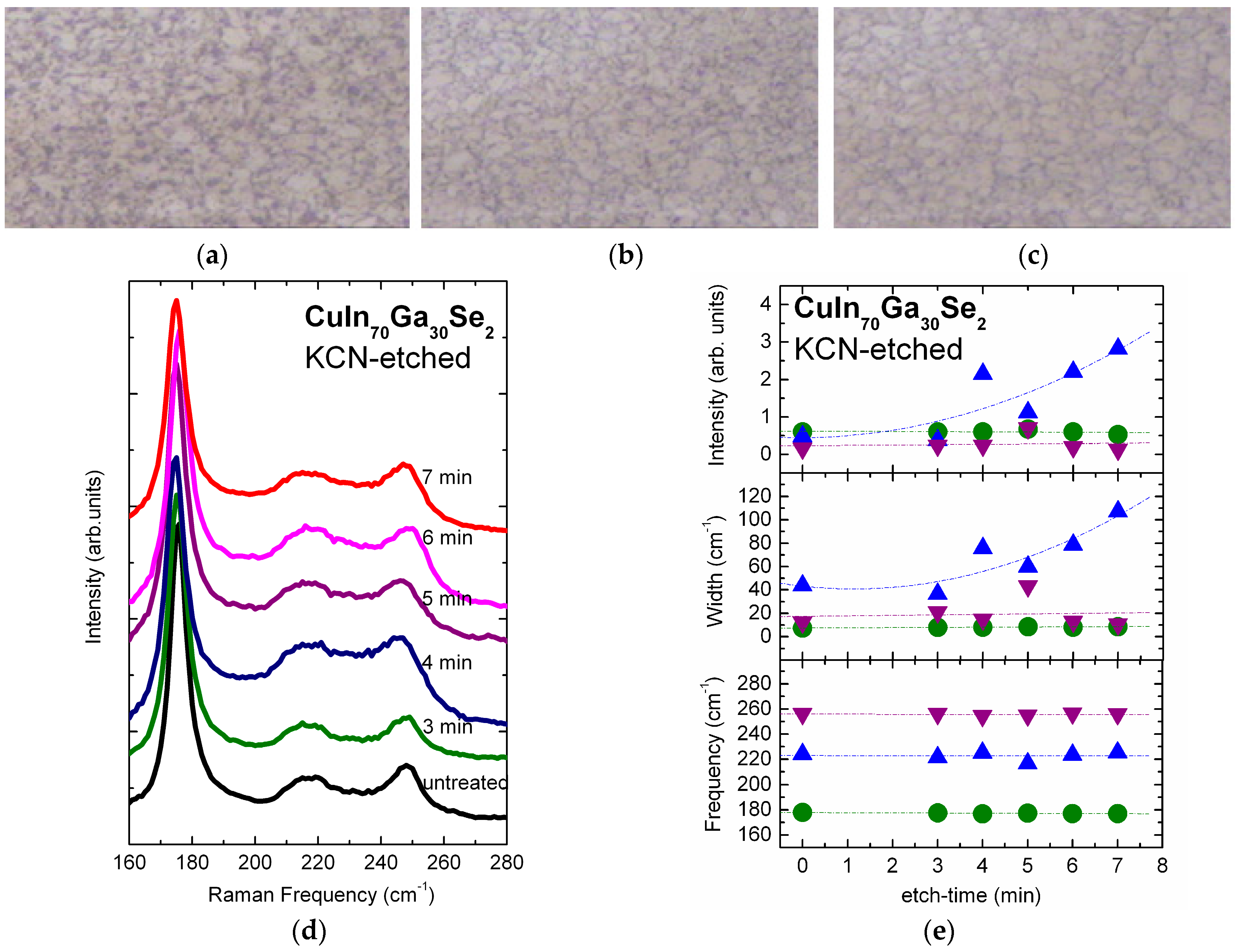
3.1. KCN-Etching of Cu(In,Ga)Se2 Surface

Secondary microcrystalline phases of copper selenide CuxSe, frequently present as selenium deficient derivatives Cu2-xSe (0.1 < x < 0.4), are usually formed on the surface of Cu-rich chalcopyrite layers. Microcrystalline CuxSe phases on chalcopyrite absorber surface introduce tensile strain, additionally to the inhomogeneous strain that the absorber exhibits as result of the lattice mismatch to the underlying substrate, and red-shift the chalcopyrite three valence-split bands: Ea, Eb, Ec [21,32] canceling thus partially the band-gap up-shift pursued by Ga addition to ternary CuInSe2 to form the quaternary Cu(In,Ga)Se2 alloy. The strain induced by CuxSe crystallites can be eliminated by wet chemical etching of the layer surface with potassium cyanide (KCN). The effect of etch-times on CuIn1−xGaxSe2 thin films, with Ga-fraction x = 0.30, used for wet-processing of ZnSe buffer- and Al:ZnO window-layer, in this work, has been investigated using Raman spectroscopy.
A brief review of lattice vibrations inclusive structural and compositional analysis of ternary and quaternary chalcopyrite solar absorbers by Raman spectroscopy is given in [33]. The mode-vibrations of the material of reference CuInSe2 are described in [34]. The vibrational frequencies of CuInSe2, CuGaSe2, and several other chalcopyrite type compounds are given in [35]. In the spectral region 150–300 cm−1, mode frequencies 174 cm−1 (A1), 217 cm−1 (B21, TO), 229 cm−1 (B11), and 231 cm−1 (B21, LO) are assigned to CuInSe2, while 183 cm−1 (A1) and 257 cm−1 (B2) to CuGaSe2. The main band frequencies are at low Ga-/high In-fractions almost equal to the Raman frequencies of the A1, B1, and B2 modes of CuInSe2 and shift with the increase of the Ga-content of the films towards the A1, B1, and B2 Raman mode frequencies of CuGaSe2. Raman modes of CuxSe crystallites dispersed on Cu-rich CuGaSe2 (or CuInSe2) surface are situated at 45 cm−1 (CuSe, Cu2Se) and 263 cm−1 (A1g) (Cu2Se) [36].
In Figure 1, the optical microscopy images (Figure 1a–c), the Raman spectra (Figure 1d), and the evaluation results of the Raman spectra (Figure 1e) of CuIn70Ga30Se2 solar absorbers studied in this work are presented in dependence of KCN etch-times ranging from 0 min (untreated absorber) through 3 min (standard etch-time) to 7 min (elongated etch-time). The Raman spectra consist of an intense, sharp peak at 177.9 cm−1 (A1) and two low intensity broad bands at 224.2 cm−1 (B1/B2) and 256.3 cm−1 (B2). While the A1 mode is in-plane vibration of anions (Se) relative to motionless cations (Cu, In, Ga), the B11 mode is a stretching in-plane vibration of anions relative to out-of-plane moving cations, and the B12 mode a totally normal-to-plane mode of both, anions and cations, moving in opposite directions. Given that the phonon mode frequencies of CuInSe2 appear blue-shifted by addition of Ga, the 224.2 cm−1 mode of CuIn70Ga30Se2 is tentatively assigned to the B12 normal-to-plane vibration. It is thus expected to respond sensitively to modifications of the symmetry-plane of motion, in this case, the chalcopyrite surface. In fact, except from the width (FWHM = full width at half maximum) of the 224.2 cm−1 mode vibration, the frequencies and widths of the observed CuIn70Ga30Se2 phonon modes are independent of etch-time (Figure 1e). It is noted, that the FWHM of the A1 Raman mode of the ternary end-members of the series, CuInS2 and CuGaSe2, is narrow at the Cu-rich and linearly broadened towards the Cu-poor/Ga-rich side as reported in [33]. The observed changes in Raman mode width as a function of [Cu]/([In] + [Ga]) ratio and the process of growth are assigned to differences in defect concentration and degree of disorder. Though unaltered for etch-times up to 3 min, the band-width (40 cm−1) of the 224.2 cm−1 mode is significantly broadened (120 cm−1) with the increase of etch-time from 3 to 7 min indicating increasing disorder in the chalcopyrite crystal lattice. Despite effective removal of surface microcrystalline phases and smoothening of surface roughness, extended etch-times concessively affect the material quality possibly due to in-depth penetration of KCN. Moreover, the optical properties of CuIn70Ga30Se2 solar absorbers, analyzed in Section 3.3.2 of the present work, are indicative of Ga enrichment in the absorber part penetrated by light, since their (optical) band gap energy of Eg (300 K) = 1.68 eV equals the gap energy of the ternary CuGaSe2 [26,32].

3.2. Structural Characterization of Al:ZnO on ZnSe/Cu(In,Ga)Se2/Mo/glass by XRD and SEM—Strain/Stress Analysis

The X-ray diffractograms include Bragg reflections on the crystallographic planes of all thin film components (CuIn70Ga30Se2 absorber, ZnSe buffer, Al:ZnO window) and the molybdenum (Mo) substrate [37]. Secondary phases of MoSe2 formed through element interdiffusion at the absorber/substrate interface are also represented. In addition, microcrystalline Cu2Se phases are still detected despite maximum KCN etch-times of 7 min, since they are spread inside the volume apart from the surface of the CIGS absorber. A ZnSe buffer is a particularly suitable material for replacement of the CdS buffer in CIGS solar technology because of its wide band gap (Eg = 2.7 eV), the minor lattice mismatch of its cubic phase to underlying CuIn70Ga30Se2 absorber (aCIGS = 5.736 Å, aZnSe = 5.669 Å), and the relatively limited mismatch of its hexagonal phase to overlying ZnO window (aZnO = 3.25 Å, aZnSe = 3.98 Å) [19]. Besides, ZnSe satisfies the conditions of band alignment at the buffer/absorber interface. Best efficiency chalcopyrite based solar cells are realized so far as heterojunctions containing a CIGS absorber. Valence and conduction band-offsets are most important parameters of a heterojunction device. In particular, the band-offsets between the absorber and the buffer layer play an important role in determining the solar cell efficiency [13,38]. Band alignment at the interface of the most commonly used buffer-layer CdS and the lower band-gap chalcopyrite absorber CuInSe2 has been thoroughly studied in [39]. Ga addition to CuInSe2 leads to increase of the absorber band-gap and band re-alignment in the vicinity of the buffer/absorber interface. In case of CdS/CuInSe2, the valence band-offset ΔEV is almost independent of the Ga-content and amounts 1 eV [40]; the conduction band-offset ΔEC, however, changes from positive (ΔEC > 0, spike) to negative (ΔEC < 0, cliff) [39]. A small spike can be beneficial because it tends to increase the inversion; a cliff is undesirable because it reduces the inversion and opens a recombination path due to the decreased barrier-height: Eb = Eg − ΔEC [13]. The barrier Eb hinders the holes from recombining with the photogenerated electrons; a decrease of Eb, thus, increases the recombination at the buffer/absorber interface [41]. To re-establish the full barrier, a buffer layer with larger conduction band-offset and/or higher band gap should be used. ZnSe fulfills both requirements. The interface characteristics and band-lineup between ZnO and epitaxial CuInSe2 (112) and (001) surfaces via formation of an ultra-thin intrinsic ZnSe buffer layer (for ZnO growth on chalcopyrites at elevated temperatures) has been investigated with photoelectron spectroscopy in [42] and was found to proceed as ubiquitous CuInX2–ZnX–ZnO (X = Se, S) structure. Band-alignment in the presence of a very thin ZnSe buffer (15–30 nm) that favors the carrier transport through the ZnO/ZnSe/Cu(In,Ga)Se2 solar structure can thus be taken for granted.

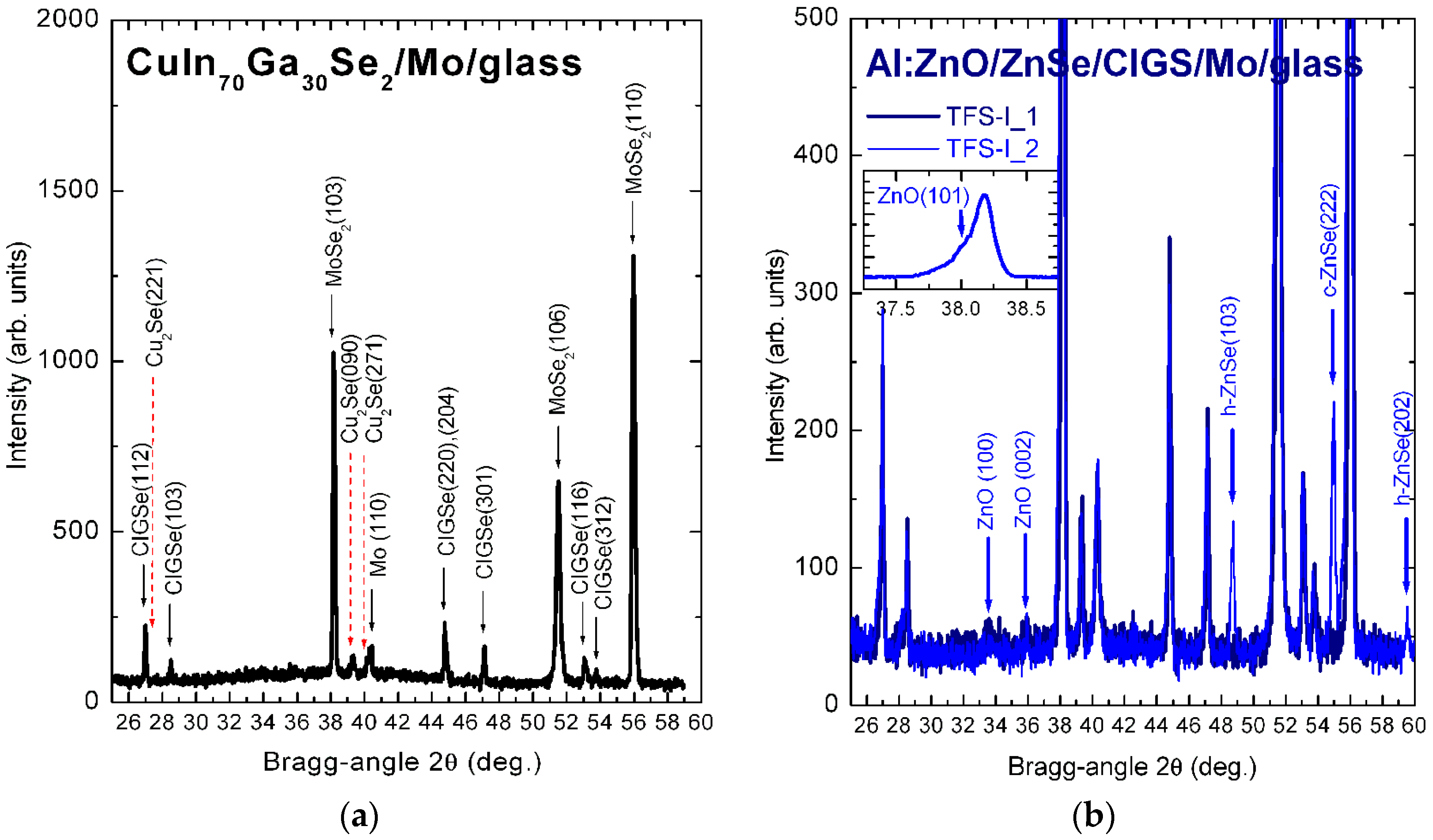
3.2.1. X-ray Diffractograms of CuIn70Ga30Se2

An X-ray diffractogram of the Al:ZnO/ZnSe/CuIn70Ga30Se2/Mo/glass solar structures is compared, in Figure 2, with the diffractogram of the CuIn70Ga30Se2 absorber on Mo/glass substrate to distinctly identify the Bragg reflections associated with the deposited buffer- and window-layers. Bragg reflections on the crystallographic planes of the polycrystalline chalcopyrite (Figure 2a) are observed at 26.98° (112), 28.48° (103), 44.76° (220), 44.86° (204), 47.10° (301), 53.06° (116), and 53.76° (312). Compared to Bragg reflections of the material of reference CuInSe2 [37,43], the reflection peaks of CuIn70Ga30Se2 are shifted to higher 2θ angles [37], because of the gallium addition in the chalcopyrite lattice, as has already been observed in both, in-vacuum grown polycrystalline ternary CuGaSe2 [44,45] and epitaxial quaternary Cu(In,Ga)Se2 [46] material modifications. The peak at 2θ = 40.34° stems from (110) crystallographic plane of the molybdenum (Mo) substrate [37]. The intense peaks at 2θ = 38.16°, 51.50°, and 55.96° are assigned, respectively, to Bragg reflections at the (103), (106), and (110) crystallographic planes of an interfacial phase of molybdenum diselenide (MoSe2) formed at the CIGS/Mo/glass interface [37,44,45]. A low intensity peak at 2θ = 39.30° inclusive supplementary peaks on the higher and lower Bragg-angle side of Cu(In,Ga)Se2 (112) and Mo (110), respectively, are assigned to reflections at the crystallographic planes of Cu2Se crystallites [37,47,48] as follows: 2θ ~27.06° (221), 39.30° (090), 40.16° (271). Copper deficient phases Cu2-xSe may also be involved at 2θ = 26.78° (111) [45].

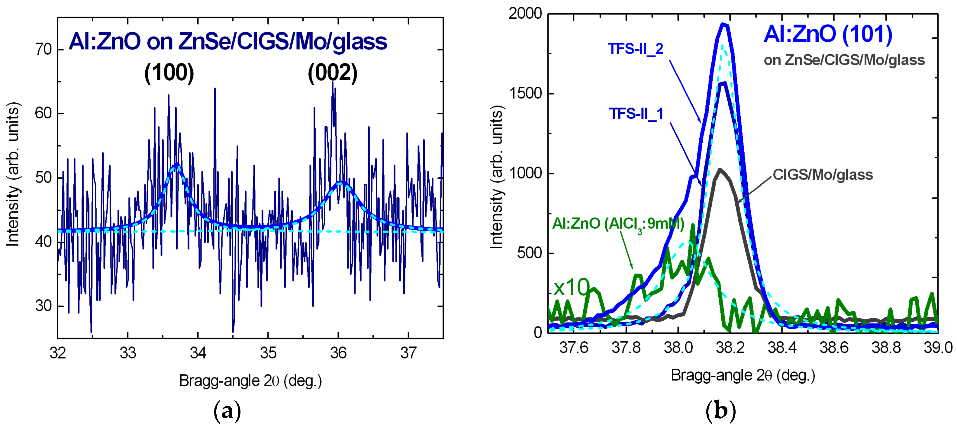
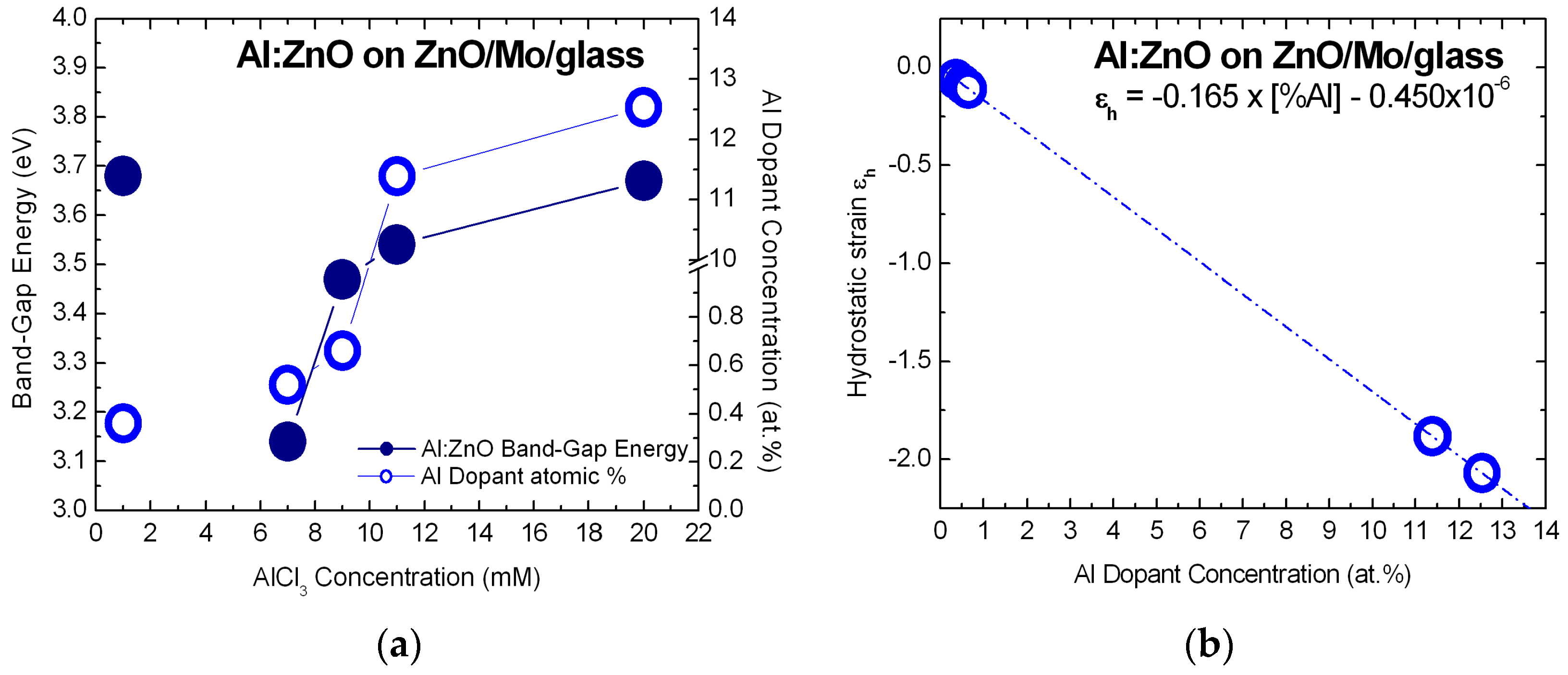
3.2.2. X-ray Diffractograms of ZnSe and Al:ZnO—Strain/Stress Analysis

A reflection peak at 2θ = 26.25° Bragg-angle is assumed to be characteristic of the presence of the ZnSe buffer. On amorphous glass and polycrystalline substrates, ZnSe is deposited with wurtzite structure (hexagonal ZnSe) and exhibits (0001) and ( 10 1 ¯ 1 ) reflections at Bragg angles 2θ ~26.3° and ~29.3°, respectively [37]. On high crystal quality substrates, epitaxial layers, and semiconductor wafers, it is preferentially oriented along the [111] crystallographic direction of the sphalerite structure (cubic ZnSe/zinc-blende type) and represented by (111) Bragg reflection at ~27.3° [37]. In case of ZnSe on Cu(In,Ga)Se2, however, the usually observed ZnSe Bragg reflection peaks [19,21] overlap with the peaks of the chalcopyrite and its secondary copper selenide phases. Low-index reflections of the very thin ZnSe buffer layer are thus overshadowed by absorber reflections. Similar holds for the aluminium doped ZnO window: low-index Bragg reflections from ( 10 1 ¯ 0 ) , (0002), and ( 10 1 ¯ 1 ) crystallographic planes in wurtzite ZnO are located at 2θ = 31.76°, 34.43°, and 36.25°, respectively, in accordance with published data [21] and data known from the literature [37]. Considering that Bragg reflection peaks of doped ZnO are shifted to higher Bragg angles with respect to the peaks of the undoped material, the peaks at 2θ = 33.68° (FWHM: 0.41°) and 36.05° (FWHM: 0.61°), in Figure 2b, are respectively assigned to the reflections on the (100) and (002) crystallographic planes of the ECD processed Al:ZnO window bilayer; the (100) and (002) reflection peaks are fitted with Lorentzians in Figure 3a. Electrochemically processed ZnO on semiconducting substrates exhibits, however, most pronounced (101) reflection shifted to higher Bragg angles with dopant incorporation as reported in [21]. The influence of dopant concentration on both, In:ZnO and Al:ZnO, has extensively been studied there for concentrations of the InCl3 and AlCl3 dopant solutes ranging from 1 to 20 mM. Depending on the dopant concentration, incorporation of In or Al in the ZnO lattice shifts the (101) reflection from nominal 2θ = 36.25° to higher Bragg angles in the vicinity of 2θ ~38.0°. The Al:ZnO (101) reflection is thus, in this case, shadowed by the absorber/substrate interference of MoSe2 (103) reflection. Peak deconvolution is possible under consideration of the carefully weighted individual contributions of substrate, epi-, and interface-layers as demonstrated in Figure 3b: the X-ray diffractogram of an Al:ZnO/ZnSe/CuIn70Ga30Se2/Mo/glass structure (TFS-II), with Al:ZnO bilayer processed successively in Zn(NO3)2 solution with 5 and 12 mM AlCl3 dopant and subjected to 2-step annealing (TFS-II_1, 350 °C, 2 h, N2-flow and TFS-II_2, 400 °C, 2 h, N2-purge), is fitted with respect to the contribution of the CuIn70Ga30Se2/Mo/glass (CIGS substrate) and the contribution of an Al:ZnO/i-ZnO/Mo/glass reference sample consisting of a bilayer of intrinsic ZnO (i-ZnO) and ZnO doped with 9 mM AlCl3. The deconvoluted peaks match excellent the individual contributions of the CIGS substrate interfacial layer and the Al:ZnO window at 2θ = 38.04° (FWHM: 0.24°).
High-index Bragg reflections (Figure 2b) emerge through successive improvement of the crystal quality of the ECD deposited Al:ZnO window and the CBD deposited ZnSe buffer successively annealed in order to maintain the chalcopyrite stoichiometry skipping selenization at elevated temperatures (T > 500 °C), which is a common feature of both, multi-stage [28,29] (T = 525 °C) and standard three-stage (T > 540 °C) [49], vacuum processes. For peak assignment at higher Bragg angles, strain induced shifts of the ZnSe and the Al:ZnO reflection peaks and relative intensity changes were taken into account. Considering that ZnSe can be grown with sphalerite (cubic) or wurtzite (hexagonal) structure dependent on substrate crystallinity and growth conditions and that high quality ZnSe buffer layers of zinc-blende structure indicated by highly intensive narrow (111) reflection peak at 2θ = 27.10° (FWHM: 0.14°) were deposited by CBD on Cu(In,Ga)Se2 absorbers after optimization of growth and post-growth annealing procedures, as reported in one of our previously published works [19], both modifications of cubic (c-ZnSe) and hexagonal (h-ZnSe) zinc-selenide were, in principle, examined. The peaks at 2θ = 48.75° and 59.54° are thus assigned to reflections on the (103) (2θ = 49.54° [37]) and (202) (2θ = 60.64° [37]) crystallographic planes of the wurtzite phase, respectively, while the peak at 2θ = 54.95° is tentatively assigned to the reflection on the (222) plane (2θ = 56.16° [37]) of the zinc-blende phase of the CBD processed ZnSe buffer layer. The shift to lower Bragg angles indicates the presence of tensile strain due to the lattice mismatch of the ZnSe epilayer (c-ZnSe, a = 5.669 Å and h-ZnSe, a = b = 3.996 Å, c = 6.550 Å) and the CuIn70Ga30Se2 substrate (a = 5.736 Å).
The interplanar spacing d was calculated from the observed reflection peaks according to Bragg’s law:
d = λ/(2sinθ)
with θ, the Bragg-angle, and λ, the Cu-Kα1 radiation wavelength (λ = 1.5406 Å). Opposite to high index planes with small spacing, planes with low indices have large spacing and pass through a high density of lattice points [50]. For the low-index reflections of ZnO, (2θ = 33.68°) d(100) = 2.659 Å, (2θ = 36.05°) d(002) = 2.489 Å, and (2θ = 38.04°) d(101) = 2.364 Å, whereas for the high-index reflections of c-ZnSe, (2θ = 54.95°) d(222) = 1.670 Å and h-ZnSe, (2θ = 48.75°), d(103) = 1.867 Å, (2θ = 59.54°), d(202) = 1.551 Å were calculated.
The grain sizes of the polycrystalline layers were obtained from Bragg-angle and -width (full width at half peak maximum (FWHM) in radians) using the Scherrer formula [50]. In polycrystalline materials, strain/stress affects primarily the peak position, while the width and the (integrated) intensity are mostly associated with the crystallite sizes, the lack of long-range order, and the degree of amorphization. Factor K = 0.9 is used for spherical crystallites, which is a common assumption in both, poly- and nanocrystalline materials:
D = K λ B cos θ
Crystallite sizes in Al:ZnO varied in the range 15–35 nm; in ZnSe, both, sizes and size-distribution, were larger: 24–74 nm. In consequence, Bragg reflections assigned to ZnSe are more intense than those of ZnO due to coagulation of small to larger size crystallites and increase of long-range order at lower temperatures of annealing in consistency with the results of ZnSe, ZnO, and doped ZnO crystallization from solutions [51,52,53].
The distance d between adjacent planes is a function of both, the plane indices (hkl) and the lattice constants. The exact relation depends on the crystal system involved [50]. For crystals of cubic symmetry (a = b = c, α = β = γ = 90ο), it has a relatively simple form:
1 d 2 = ( h 2 + k 2 + l 2 a 2 )
For crystals of hexagonal symmetry (a = bc, α = β = 90°, γ = 120°), the d-spacing is given by:
1 d 2 = 4 3 ( h 2 + h k + k 2 a 2 ) + l 2 c 2
The lattice constants of both, ZnSe buffer and Al:ZnO window, can thus be determined from the respective X-ray diffractograms and Equations (6), (8) and (9). Principally, the lattice constants of thin films and doped solids differ from those of bulk crystals since they succumb to the effects of hydrostatic and/or mismatch strain [21,31,54]. The lattice constants of ZnO (a = 3.070 Å and c = 4.979 Å) calculated with Equation (9) as a = ( 2 3 / 3 ) d , from d(100) = 2.659 Å, and c = 2d, from d(002) = 2.489 Å, are smaller than those known from the literature (bulk values: a = 3.250 Å and c = 5.207 Å [37]) indicating the existence of (hydrostatic) compressive strain in the ZnO lattice through Al-dopant incorporation. Moreover, the d-spacing of the (101) reflection obtained as d = a c 3 / ( 3 a 2 + 4 c 2 ) = 2.35 Å from Equation (9) and the calculated values of a, c, complies, within experimental and calculation errors, with the measured d(101) = 2.36 Å, which further confirms the ZnO reflection peak assessment.
The strains described by Equations (A2), (A3), (A16) and (A17) in Appendix A can be linearly superimposed to give the effective strain [55]:
ε a , e f f = [ a ( a 0 Δ a ) ] / ( a 0 Δ a )
ε c , e f f = [ c ( c 0 Δ c ) ] / ( c 0 Δ c )
In this representation, a 0 Δ a = a 0 ε h a 0 = a e p i , e f f and c 0 Δ c = c 0 ε h c 0 = c e p i , e f f are the “effective” lattice constants of the Al:ZnO epilayer as calculated from the experimentally measured X-ray diffractograms. The hydrostatic and “effective” mismatch strain can thus be determined in accordance with:
ε h ( a e p i , e f f ) = a e p i , e f f a 0 a 0 , ε h ( c e p i , e f f ) = c e p i , e f f c 0 c 0
ε a , e f f = a s u b a e p i , e f f a e p i , e f f
ε c , e f f = c s u b c e p i , e f f c e p i , e f f
The respective in-plane and surface-normal stresses related to hydrostatic strain are:
σ x x = σ y y = ( C 11 + C 12 + C 13 ) ε h
σ z z = ( 2 C 13 + C 33 ) ε h
The “effective” stress associated with both, the hydrostatic and mismatch strain, can be determined by inserting the “effective” strain components εa,eff and εc,eff, from Equations (13) and (14), in Equations (A14) and (A15) instead of the strain components εa and εc defined by Equations (A2) and (A3).
Hydrostatic strain effects related to Al-dopant incorporation in the ZnO lattice were quantified in one of our recent publications [21]. The Al:ZnO reference layers were deposited by ECD with thickness ~400 nm (deposition time: tdep = 300 s) on ~40 nm ECD processed ZnO templates on Mo/glass substrates. The lattice mismatch between the hexagonal ZnO template (a = b = 3.250 Å) and the cubic Mo substrate (a = 3.147 Å) is ~3%. The mismatch of the Al-doped ZnO window (a = 3.070 Å) to the hexagonal-phase of the ZnSe buffer (a = 3.996 Å) is significantly higher (~30%) and particularly high (90%), when compared to its cubic-phase (a = 5.784 Å); it is thus anticipated that part of the shift to higher Bragg angles generated by (hydrostatic) compressive strain (εh) in Al:ZnO is cancelled by the tensile mismatch strain to the underlying ZnSe. Doping of Al:ZnO on i-ZnO/Mo/glass reference layers with 9 mM AlCl3, results in εh = −0.11. The hydrostatic strain is radically increased to εh = −1.88 by an increase of the solute dopant concentration to 11 mM, e.g., by surpassing the 10 mM “threshold” detected in [21]. Nevertheless, higher dopant concentrations and dopant induced strains can be assimilated without coalescence breaking and fracturing of the layer microstructure by increasing the thickness of the layer and thus modifying the spatial dopant distribution. In accordance with the thickness versus solute-dopant-concentration calibration performed there, the Al:ZnO bilayer successively processed with 5 and 12 mM AlCl3, in the present study, consists of a highly-doped 1st-layer with thickness ~400 nm and an ultra-highly-doped 2nd-layer with thickness ~600 nm both represented by a reflection peak at Bragg angle in the immediate vicinity of the angle of the Al:ZnO reference layer doped with 9 mM AlCl3. It may thus be assumed, that εh ≤ −0.11. In fact, the hydrostatic strain calculated with Equation (12) from the measured lattice constants of the Al:ZnO window layer (a = 3.070 Å and c = 4.979 Å) and the lattice constants of bulk ZnO (a = 3.250 Å and c = 5.207 Å [37]) by using the elastic stiffness constants of ZnO known from the literature (C11 = 190 GPa, C12 = 110 GPa, C13 = 90 GPa, C33 = 196 GPa [56]) is εh = −0.050 (εh(aepi,eff) = −0.055, εh(cepi,eff) = −0.044). Based on the volume density of host N(ZnO) = 8.30 × 1022 cm−3 and substitute N(Al) = 6.03 × 1022 cm−3, the percentage of Al3+ cations (rAl = 1.82 Å) that occupy sites of Zn2+ cations (rZn = 1.53 Å) in the Al:ZnO lattice introducing internal hydrostatic strain and lattice contraction of magnitude b = −2.74 × 10⁻²⁴, because of the larger size of Al with respect to Zn, can be deduced from Equations (A16) and (A17): C (C%) = 30%, N(Al) = 1.81 × 1022 cm−3. The respective in-plane and surface-normal compressive stresses calculated with Equations (15) and (16) are: σxx = σyyzz~−19 GPa. A stress value of this order (−21 GPa) can also be obtained in case that the bulk modulus of ZnO (B = 142.4 GPa [57]) is used to describe the lattice compression under the assumption that the only effect of volume deformation will be the decrease of the lattice constant of the overall system [58]:
p = B Δ V / V = 3 B Δ a / a = 3 B ( a 0 a e p i , e f f ) / a 0
In layered structures, however, the effect of hydrostatic pressure may lead to non-uniform deformation, since the c-axis may decrease, under pressure, stronger than the a-axis indicating that the out-of plane compression is stronger than the in-plane compression [59]. Under the application of hydrostatic pressure:
σ x x = σ y y = σ z z = σ ,   σ x y = σ y z = σ z x = 0
calculation in accordance with Equation (A4) yields:
ε x x = ε y y ( = ε a ) = ε
ε z z ( = ε c ) = C 11 + C 12 2 C 13 C 33 C 13 ε
σ = [ C 33 ( C 11 + C 12 ) 2 C 13 2 C 33 C 13 ] ε
Considering the ratio of the strain components in the direction of the surface-normal and in the plane-of-surface ε c / ε a , as defined in the cases of:
(a1)
biaxial in-plane stress, in Equations (A12) and (A13), ε c ε a = ( ) 2 C 13 C 33 = ( ) 0.918 ,
(a2)
uniform pressure, in Equations (19) and (20), ε c ε a = C 11 + C 12 2 C 13 C 33 C 13 = 1.132 ,
and measured experimentally in the cases of:
(b1)
effective strain εa,eff, εc,eff, in Equations (13) and (14), ε c ε a = 1.046 ,
(b2)
effective hydrostatic strain εh(aepi,eff), εh(cepi,eff), in Equation (12), ε c ε a = 0.800 ,
the almost equal changes of strain loads (absolute values) in (a1), (a2), Δ ε c ε a = 0.214 , calculated exclusively in dependence of material elasticity, and in (b1), (b2), Δ ε c ε a = 0.246 , experimentally observed, indicate that non-uniform hydrostatic lattice compression may eventually take place in ECD processed Al:ZnO on ZnSe/CuIn70Ga30Se2/Mo/glass solar structures, a portion of which is counterbalanced by the tensile stress field of mismatch strain between the Al:ZnO window and the underlying ZnSe buffer. The effective bisotropic tensile stress ascribed to the mismatch strain between the ZnSe intermediate layer (a = 3.996 Å, c = 6.550 Å) and the compressively through doping strained Al:ZnO epilayer (a = 3.070 Å and c = 4.979 Å) was calculated with Equation (A14) to σeff ~65 GPa; this is higher than the bisotropic tensile stress σ ~50 GPa between ZnSe and undoped ZnO by 30% which equals exactly the percentage C% = 30% of Al3+ substitutes in the Al:ZnO lattice calculated with Equations (12), (A16) and (A17).
The lattice constant of cubic ZnSe (bulk value: a = c = 5.669 Å [37]) calculated with Equation (8) from Bragg reflection on (222) crystallographic plane with interplanar spacing d(222) = 1.670 Å is a = 5.784 Å. The lattice constants of hexagonal ZnSe (bulk values: a = 3.996 Å and c = 6.550 Å [37]) calculated with Equation (9) from (103) and (202) reflections with d-spacing d(103) = 1.867 Å and d(202) = 1.551 Å are a = 4.058 Å and c = 6.609 Å. In both cases, c-ZnSe and h-ZnSe, the lattice constants of nm-thick ZnSe buffer on μm-thick Cu(In,Ga)Se2 absorber are by 1%–2% larger than the respective lattice constants of the bulk indicating the presence of tensile mismatch strain ε (=εxx) of this order with respect to the underlying CuIn70Ga30Se2 layer (a = 5.736 Å and c = 11.448 Å [37]) thus lattice-stretching εxx = (5.736 − 5.669)/5.669 dominated by the cubic phase of ZnSe. The respective tensile stress calculated by inserting the strain values and the elastic stiffness constants of c-ZnSe known from the literature (C11 = 85.7 GPa, C12 = 50.7 GPa, C44 = 40.5 GPa [60,61]) in Equation (A14) is σ ~1.5 GPa.

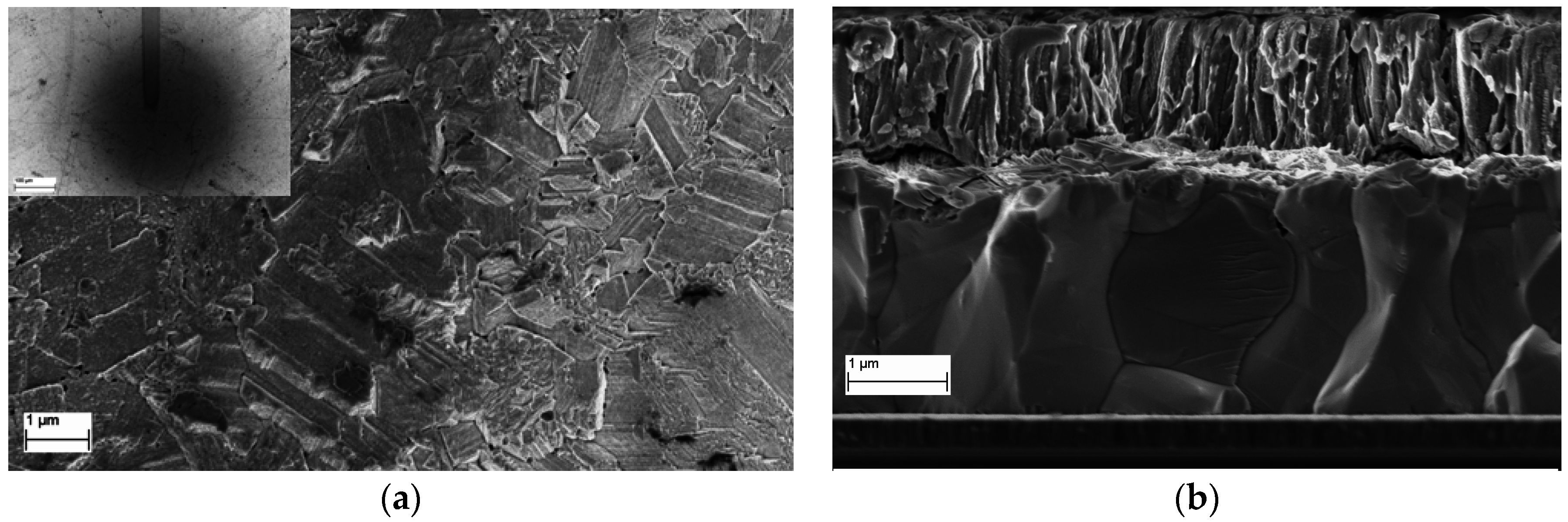
3.2.3. SEM Images of Al:ZnO

The surface morphology and preferential growth of Al:ZnO bilayers along the ( 10 1 ¯ 1 ) crystallographic direction are depicted in the SEM micrographs of Figure 4a,b. Except from preferential orientation evidenced through SEM imaging on the cross-section of the bilayer, oriented growth along (101) is strongly suggested by the ×20 higher intensity of Bragg reflection on the (101) crystallographic plane of Al:ZnO (Figure 3b), following peak deconvolution, in comparison with the intensities of the (100) and (002) reflections (Figure 3a). Hence, the SEM images of the ECD processed bilayer show surface texturing under preferred 45° and distinct c-axis orientation expected to facilitate both, optical and transport properties across the layers.
Oriented growth up to self-organized growth in the form of ZnO nanorods [62,63,64] is assumed to be among others precipitated in the presence of strain. The stress due to the lattice mismatch between nanorods and substrates and the surface roughness of the layer underneath of the nanorods essentially influence the formation of ZnO nanorods [65]. Moreover, improved light harvesting performance was reported [66] for the selective heteroepitaxial growth of ZnO nanorods via formation of ZnO seeds anchoring to the nanorod outer TiO2 substrate surface with lattice modulation presumably induced by the strain from the lattice mismatch. In chalcopyrite absorber based thin solar cells with ultra-thin buffer layer, both, the lattice mismatch of the highly doped ZnO window to underlying absorber layer and the orientation of the chalcopyrite layer itself, are anticipated to contribute to the oriented growth of the ZnO window and front-contact layer. According to published literature [67], high efficiency absorbers grown on standard Mo-coated soda-lime glass (Mo/SLG) substrates are clearly and unambiguously (110) oriented, whereas, in Na-free polycrystalline Cu(In,Ga)Se2 thin films grown on Mo foils, grains with both orientations (110/102) are present. It is commented [67], that devices with efficiency >18%, all show a certain degree of (110) preferred orientation of the absorber film.

3.3. Optical Characterization of Al:ZnO on ZnSe/Cu(In,Ga)Se2/Mo/glass by NUV-VIS-NIR Spectrophotometry

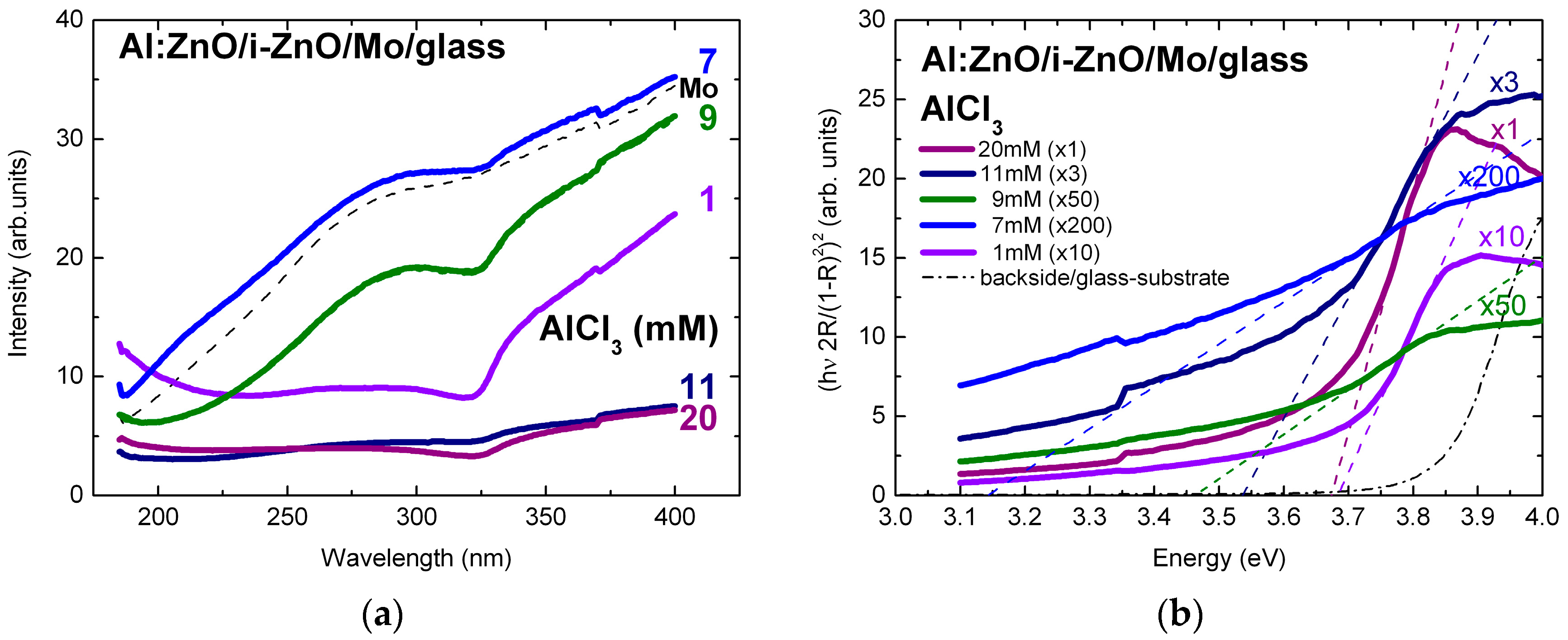
3.3.1. Optical Characterization of Al:ZnO/ZnO Reference Samples on Mo/glass

Aluminium doped zinc oxide (AZO) films represent a promising upcoming alternative to transparent conductive oxide (TCO) films mainly because of their competitive electrical and optical properties, cheap and abundant raw materials, nontoxic nature, long term environmental stability, and easy fabrication. The structural and electrical properties of Al:ZnO/ZnO bilayers deposited by ECD on Mo/glass substrates as preliminary test-structures for the ECD growth of lightly-to-highly doped Al:ZnO bilayers on CIGS photovoltaic absorbers were reported in one of our previous publications [21]. It was found, that through dopant incorporation, the Al:ZnO layers exhibit high hydrostatic compressive strains in the range εh = (−0.059)–(−2.071). The optical properties of these test-structures are thoroughly being reconsidered, in the present work, since Al substitutes (or interstitials) in the ZnO lattice and thereby induced built-in strain of Al:ZnO may considerably affect the band-gap energy and hence the transparency of the Al:ZnO window layer of CIGS TFSCs.
The reflectance spectra of Al:ZnO/ZnO bilayers were recorded in the NUV-VIS region from 180 to 400 nm. As demonstrated in Figure 5a, the surface reflectivity varies in the range 5%–35% (normalized intensity) with varying the AlCl3 solute dopant concentration of the ECD process from 1 to 20 mM and reaches, at 7 mM, a maximum comparable with the reflectivity of the molybdenum back contact over the measured spectral range. Further increase of the ECD precursor concentration, particularly above 10 mM, is followed by decrease of the spectral reflectance through increasing surface roughness possibly because of strain induced surface faceting up to coalescence breaking as observed in [21]. Despite spatial variations up to 10% associated with local variations of surface roughness, curvature changes associated with the spectral reduction of reflectance through absorbance at (optical) band-gap energy of Al:ZnO are evidenced throughout the concentration changes of solute dopant from low (1 mM) to extra-high (20 mM). The (optical) band gap of the Al:ZnO/ZnO test structures was extracted from the reflectance spectra similarly to [21] by using the Kubelka-Munk approximation referred in [68,69]. The evaluation principles are briefly reviewed in the following:
The so-called diffuse (or volume) reflection, in polycrystalline materials, results from the reflection, refraction, diffraction, and absorption by crystallites oriented in all directions. Based on the absorption (K) and scattering (S) per unit layer thickness of the medium assumed to be a continuum, in the limiting case of an infinitely thick sample, the Kubelka-Munk equation at any wavelength becomes:
K S = F ( R ) = ( 1 R ) 2 2 R
where F(R) is usually termed the remission or Kubelka-Munk (K-M) function. To fulfill the condition set to layer thickness and enable the K-M approximation, the layers should be grown thick enough to ensure that a further increase in thickness will fail to change the reflectance.
In the parabolic band approximation, band-gap Eg and absorption coefficient α of a direct band-gap semiconductor are related through the well-known equation [70]:
α h ν = C ( h ν E g ) 1 / 2
where α is the linear absorption coefficient of the material, hν is the photon energy, and C is a proportionality constant.
Considering the K-M absorption coefficient K as proportional to α and the K-M scattering coefficient S as wavelength independent constant, the sample absorption in Equation (23) can be expressed in terms of the inverse remission function of Equation (22) as follows:
( ( F ( R ) ) 1 h ν ) 2 = C ( h ν E g )
A plot of ((F(R))−1 hν)2 in dependence of energy (hν), with F(R) calculated according to Equation (22), and linear fit up to the point of curve inflection gives by intersection with the energy axis the band gap energy of the sample. The linear fits of the absorption edges of the Al:ZnO overlayers are depicted in the tauc-plots of Figure 5b with the AlCl3 solute dopant concentration 1–20 mM as parameter. The respective band gap energies are in the range: Eg(Al:ZnO) = 3.14–3.68 eV. The experimental and calculation errors have magnitude ±0.05 eV.
The distribution of gap energies is a result of the competition between two reciprocal interdependent effects: band-gap narrowing through increase of donor-level population and band-gap widening under the influence of compressive stress generated by the incorporated Al-donors. Referred to the Al-doping induced disorder and the Al-defects, several competing, if not incompatible, structural models have been proposed. Only point defects have been considered so far, although a much wider variety of defects, like edge and screw dislocations or planar and volume defects, seem to be possible. An overview of the suggested defects in Kröger-Vink notation [71] is given in [72]. Most works consider aluminium substituting for zinc (AlZn) to be a likely defect impinging thus the material band-gap. Neutral defects involving three Zn2+ cations replaced by two Al3+ cations and a compensation cationic vacancy and acting as electrons traps have also been discussed [73]. Recently published micro-Raman, X-ray photoelectron spectroscopy (XPS), and spectroscopic ellipsometry (SE) analyses of Al:ZnO films prepared by co-sputtering of ZnO and Al at moderate temperatures (RT-188 °C) [74] indicate that the incorporated host-atoms are Al3+ species in Zn2+ substitutional position and their amount increases following a direct monotonic trend with the deposition temperature. For liquid-phase processing of Al:ZnO/ZnO by ECD, at 80 °C, the dependence of band-gap energy on AlCl3 solute dopant concentration and the respective atomic percent (at. %) of aluminium incorporated in the ZnO lattice, as determined by energy dispersive analysis X-ray (EDAX) in [21], is demonstrated in Figure 6a. The dependence of band-gap energy on hydrostatic compressive strain generated by Al-dopant incorporation is indirectly accessed using the strain εh versus Al (at. %) relation of Figure 6b:
εh = −0.165 × [%Al] − 0.450 × 10⁻⁶
For solute dopant concentrations below the 10 mM “threshold” detected in [21], introduction of Al3+ dopant inside the ZnO lattice is difficult from natural coordination preference [72,73,74] and leads consequently to very low solubility limit (<1 at. %). The effect of low Al content of Al:ZnO is apparently defect related band-gap narrowing from Eg = 3.68 to 3.14 eV (Figure 6a). With the increase of AlCl3 concentration in the ECD solution, the atomic fraction of Al in the ZnO lattice is successively increased, the hydrostatic compressive strain is simultaneously being increased (Figure 6b) and takes over in the vicinity of the 10 mM “threshold” with one order of magnitude higher Al content (>10 at. %) leading to reestablishment of the initial band-gap energy (Figure 6a).

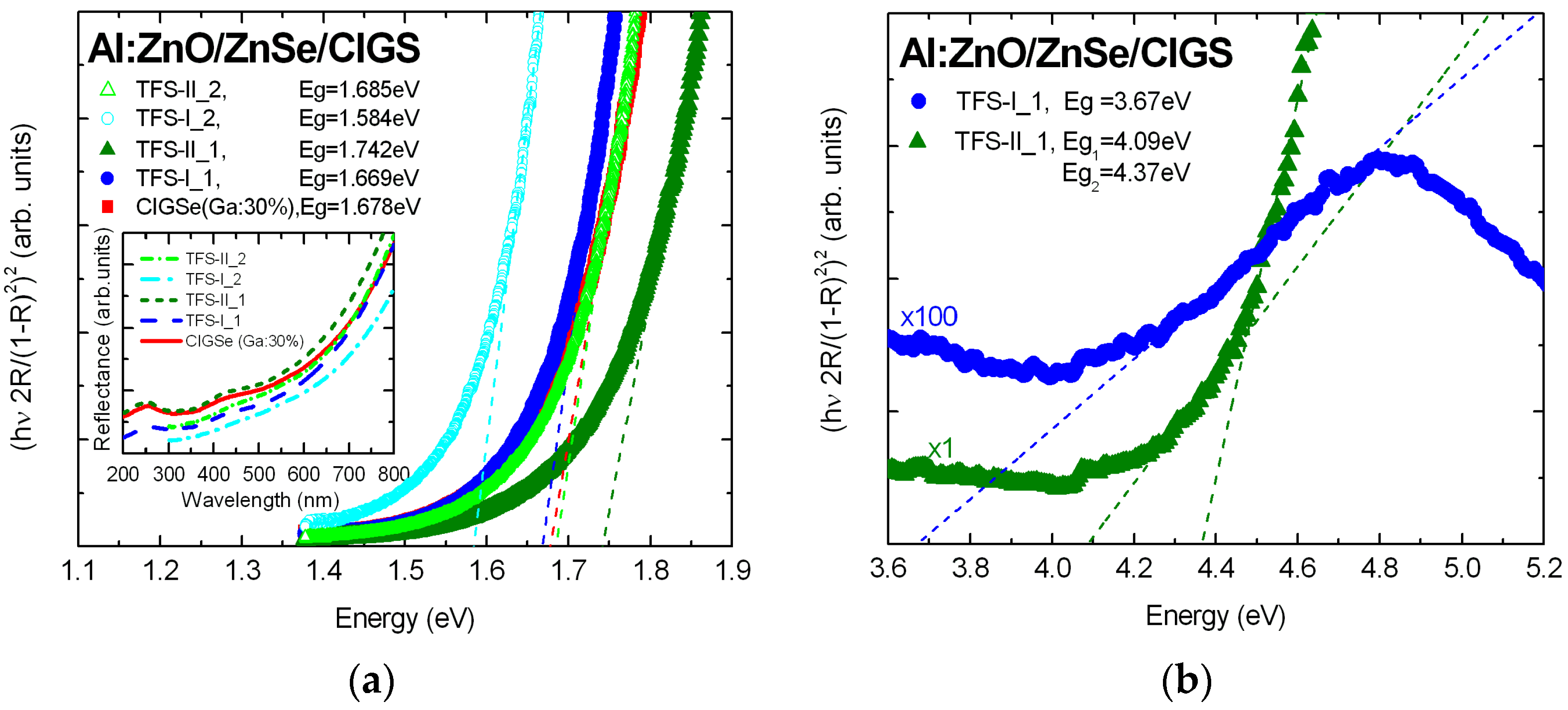
3.3.2. Optical Characterization of Al:ZnO on ZnSe/Cu(In,Ga)Se2/Mo/glass Solar Structures

The solar Al:ZnO/ZnSe/CuIn70Ga30Se2 thin film structures (TFS) on Mo/glass substrates were of two different types: TFS-I and TFS-II according to process modifications of chalcopyrite absorber and ZnSe buffer, prior to Al:ZnO deposition by ECD, predestined to modify significantly the TFS properties. In TSF-I, the chalcopyrite absorber surface was subjected to additional treatment by KOH following KCN etching; besides, the deposition time of the ZnSe buffer layer by CBD was reduced to 2/3 of standard duration 90 s aiming to minimize the layer thickness in accordance with optimization criteria reported in [19,75]. The NUV-VIS-NIR spectral reflectance of TFS-I and TFS-II, depicted in the inset of Figure 7a, was recorded following each annealing step. As described in Section 2. Materials and Methods, the solar structures were annealed in two steps aiming to produce high quality polycrystalline ZnO-window/ZnSe-buffer by maintaining the stoichiometry of the selenium buffer/absorber compounds: 1-step: 350 °C, 2 h, N2-flow (TFS-I_1, TFS-II_1) and 2-step: 400 °C, 2 h, N2-purge (TFS-I_2, TFS-II_2). For comparison, the reflectance of bare CuIn70Ga30Se2 absorber subjected to KCN-etching, with etch-time (7 min) equal to that of absorbers processed to solar structures, is also shown. The reflectance of TFS-I_1 is lower at NUV and converges to CIGS reflectance at NIR opposite to the TFS-II_1 being equal to CIGS reflectance at NUV and higher at NIR. The reflectance of both, TFS-I_2 and TFS-II_2, is reduced following the 2-step of annealing; the TFS-II_2 reflectance is then lowered at NUV and becomes equal to CIGS reflectance at NIR. It is assumed that, among other factors such as strain, surface oxidation, and Se depletion, these reflectance changes are the result of annealing induced changes of the microstructure associated with bond-/angle-rearrangement, improvement of long-range order, and transparency enhancement in the window/buffer layers of the layer sequence studied. The reflectance spectra of the solar structures were evaluated similar to the former case of Al:ZnO/ZnO test structures using the Kubelka-Munk approximation and tauc-plots of CuIn70Ga30Se2 absorber, in Figure 7a, and Al:ZnO bilayer, in Figure 7b.
The absorption-edge of the bare CIGS absorber, with 30% Ga fraction and Ga enrichment in the upper layer part by exposure to elongated KCN etch-time, and thus its band-gap energy is shifted to Eg(CIGS) = 1.678 eV. With reference to this energy, the band-gap energies of TFS-I_1 and TFS-II_1 appear, following the 1-step of annealing, red-(Eg(CIGS) = 1.669 eV) and blue-shifted (Eg(CIGS) = 1.742 eV), respectively. Considering that the CIGS absorber (2.4 μm) and the Al:ZnO window (1.2 μm) have comparable thickness, the band-gap broadening of the TFS-II_1 absorber is tentatively assigned to the compressive stress that the chalcopyrite experiences from the Al:ZnO overlayer. The ZnSe buffer is probably, at standard CBD process time 90 s, already too thin to act as an ideal “wetting” layer and fully relax strain. This kind of compressive stress exhibits also TFS-I_1; the band-gap narrowing is, in this case, mainly due to mild surface oxidation by KOH; this results in a surface that is rich in polyselenides ((Se2−)n) with a few copper hydroxides due to the dissolution of metal ions from the surface and near surface layer parts as observed in ambient air, acidic, and alkaline conditions by X-ray Photoelectron Spectroscopy (XPS) in [76]. In aqueous solution, the selenide ion (Se2−) is prevalent only in very basic conditions. In neutral conditions, hydrogen selenide ion (HSe) is most common. In acid conditions, hydrogen selenide (H2Se) is formed. In flotation related conditions, polyselenide species and more selenate species are found at the chalcopyrite surface after oxidation [77]. Production and release of selenates (SeO24−) from oxidized surfaces is thus implicated in the uptake of selenate on alkaline oxidised chalcopyrite. Selenates are highly soluble in aqueous solutions, at ambient temperatures. The band-gap narrowing of TFS-I_1 can thus be explained as originating from selenium deficiency. In analogy, the red-shifts of the band-gap energies of TFS-I_2 (Eg(CIGS) = 1.584 eV) and TFS-II_2 (Eg(CIGS) = 1.685 eV), after the 2-step of annealing, can be interpreted as due to losses of volatile Se element. Band gap narrowing by annealing in inert gas (Ar) or forming gas (N2 + H2) instead of selenium atmosphere is a common effect systematically analyzed in scientific research studies in the past [78]. The results of the present study imply that the net-effect amounts 5% for TFS-I_2 and remains almost unnoticed in TFS-II_2 CIGS absorber. Analysis of the high energy spectral part of the reflectance by Kubelka-Munk and tauc-plot formalism yields, for the band-gap energy of the Al:ZnO window bilayer of TFS-I_1, Eg(Al:ZnO) = 3.67 eV equal to gap energy of highly doped strained Al:ZnO/ZnO test-structures discussed in part A) of this section. In TFS-II_1, the strain accumulated in the bilayer shifts the absorption edge above 4 eV and two contributions with Eg(Al:ZnO) = 4.09 eV and Eg(Al:ZnO) = 4.37 eV assigned to the Al:ZnO sub-layers with lower (5 mM) and higher (12 mM) doping can be distinguished.

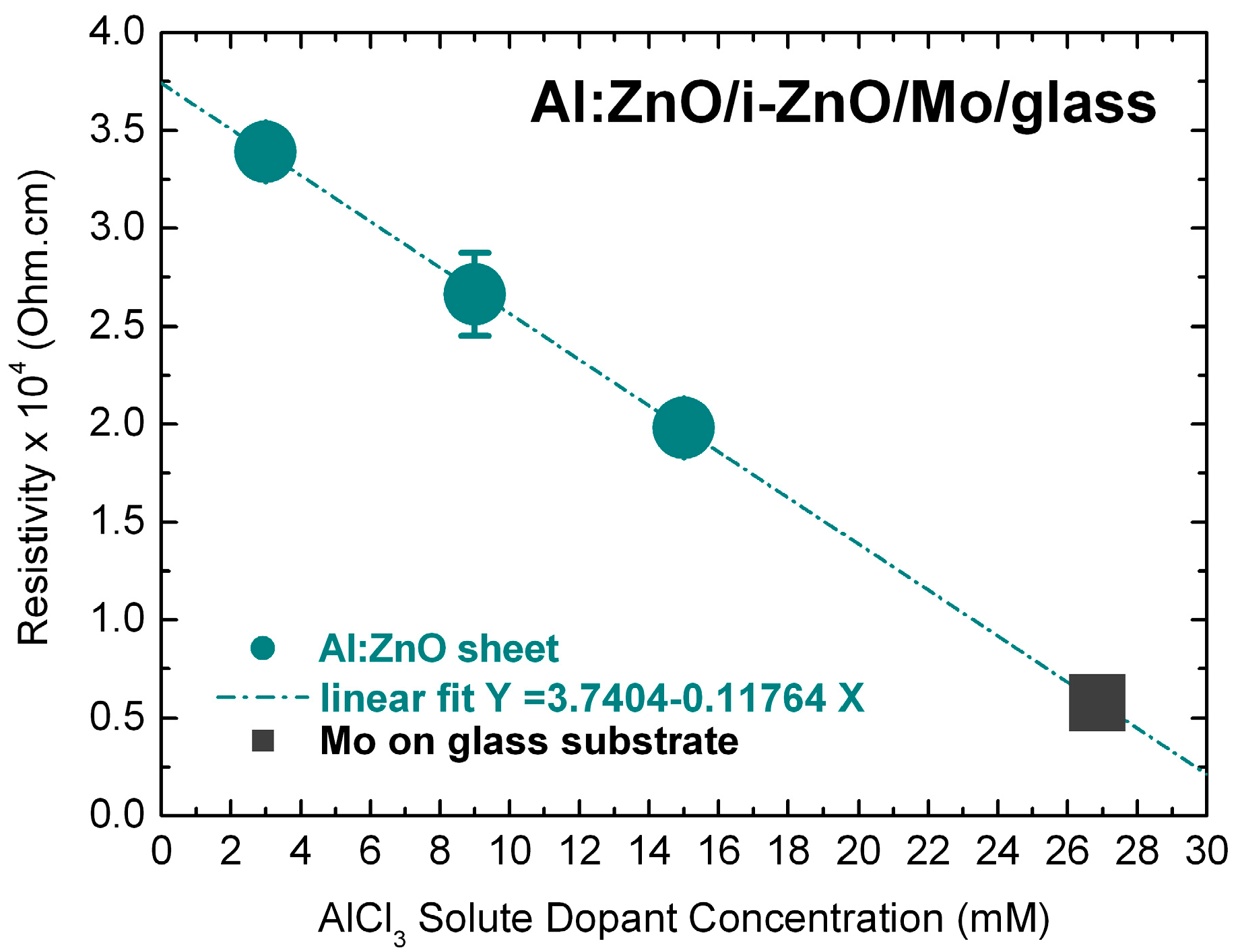
3.4. Electrical Characterization of Al:ZnO on ZnSe/Cu(In,Ga)Se2/Mo/glass by van-der-Pauw and I-V Measurements

In CIGS solar cells, it is customary to use a high-low resistivity grading of the ZnO layer: An undoped layer of ZnO with higher resisitivity is initially deposited on the buffer layer followed by deposition of a doped low resistive layer. Achieving resistivity control while maintaining adequate transparency of films usually sputtered from two separate targets is not trivial. Moreover, a study of the properties of CIGS solar cells with [Ga]/([In]+[Ga]) ratios ranging from 0.26 to 0.31 strongly suggests that highly efficient cells can be fabricated without using the high-resisitivity undoped ZnO layer even in case of very thin buffer layer [79]. Opposite to sputtering processes, wet processing by ECD allows convenient doping and thus resistivity grading by varying the solute dopant concentration.
In one of our previous publications [21], ECD processed Al:ZnO/i-ZnO on Mo/glass and In:ZnO/i-ZnO on ZnSe/Mo/glass test-structures were probed. The intrinsic conductivity ZnO layer (i-ZnO) has been proven in [80] to inhibit leakage currents. The i-ZnO layer thickness of chalcopyrite based thin film solar cells, however, should not exceed 70 nm, otherwise the serial resistance is increased and the fill factor of the cell derogates [80]. The electrical resistance of the Me/Al:ZnO/ZnO/Mo/glass layer sequence (sequential resistance), in [21], was determined from the current versus voltage (I(V)) characteristic curves measured between the molybdenum back contact and the front metal carrier-collector. The I-V measurements of the Au/Ni/Al:ZnO/ZnO/Mo/glass test-structures comprise resistivity values of (0.46 − 1.33) × 105 Ω·cm dependent on the AlCl3 solute dopant concentration (1-20 mM). The sequential resistance is in this case mainly due to undoped ZnO layer and to a minor degree still influenced by the Al-doped ZnO layer as expressed by the Al:ZnO/ZnO resistivity versus AlCl3 concentration calibration-curve in [21]. The electrical conductivity of aluminium doped zinc oxide materials (AZO) depends on doping induced defects and grain structure. AlZn substitutes contribute with 1e to the increase of local charge density. Al interstitials, tetrahedrally or octahedrally coordinated to O sites, offer already 3e [72].
Sheet resistance measurements performed, in the present work, on In-pellet contacted highly doped Al:ZnO sheets deposited by ECD on ZnO/Mo/glass from Zn(NO3)2 solution with AlCl3 solute dopant in the range 3–15 mM yielded resistivity values in the order of 10−4 Ω·cm as demonstrated in Figure 8; the resistivity of the Al:ZnO sheet processed with 9 mM AlCl3 was ρ(Al:ZnO) = (2.7 ± 0.2) × 10−4 Ω·cm. The sheet resistance of 400 nm thick molybdenum on glass substrate (Mo/glass) used to process the Al:ZnO/ZnO reference samples by ECD and also used as standard back contact of CIGS TFSCs was found to be of the same order: ρ(Mo) = 0.58 × 10⁻⁴ Ω·cm and is inserted in Figure 8 for comparison reasons. This value is exactly one order of magnitude higher than the molybdenum bulk resistance known from the literature: ρ(Mo) = 0.58 × 10⁻⁵ Ω·cm at 300 K [81]. Sputtered molybdenum films of thickness 0.5 μm and good adhesion to soda-lime glass for CIGS device technology exhibit usually resistivity values by factor 5–10 higher than the resistivity of the bulk [82,83]. Hence, an ultra-heavily doped Al:ZnO front contact of a CIGS TFSC deposited from ECD solution with 27 mM AlCl3 is expected to be equally conductive to molybdenum back contact.
Least resistance path calculations (Appendix B) performed in the present configuration of the Al:ZnO/i-ZnO/Mo layer sequence with dimensions 0.4/0.9/0.4, 0.7/1.4/0.4, and 0.8/1.0/0.4 μm and resistivities of the i-ZnO and Mo films of order 105 and 10−4 Ω·cm, respectively, exclude interferences of the low resistive Mo coating of the glass substrate in the determination of the sheet resistance of highly doped Al:ZnO assuming that its resistivity is of order 10 and lower. At present, compilation of literature data of the electrical properties of ZnO films prepared by various deposition techniques and doped with the group IIIB elements B, Al, Ga, and In [84] shows that resistivities obtained with Al dopant do not exceed 10−2 Ω·cm. The lowest resistivities of polycrystalline ZnO films deposited by magnetron sputtering, metal organic chemical vapour deposition, and pulsed laser ablation were found to be in the range of 1.4–2.0 × 10⁻⁴ Ω·cm [85]; the resistivity of ECD deposited highly doped ZnO films is of the same order. Normalized to Mo bulk resistance, highly doped ZnO liquid-phase deposits may exhibit resistivity of the order 10−5 Ω·cm at the low limit. An upper limit of the order 105 Ω·cm is set by the resistivity of (intrisic) ZnO previously discussed. This can further be reduced towards the resistivity of undoped bulk ZnO of order 10 Ω·cm reported in the literature [86] by fine adjustment of the ECD process parameters, in particular the electrochemical potential EC, and the parameters of the subsequent annealing procedure.
Van der Pauw measurements suitable for low and accurate resistance determination by minimization of the spreading and contact resistance [87,88,89] were additionally performed on Al:ZnO doped with 3 mM AlCl3 and yielded resistivity of order 10−5 Ω·cm, thus confirming the low-resistive nature of the layers, as detected by the two-point measurement technique. In the microscale, the dimensionless R* electrical contact resistance (ECR) of conductive rough surfaces depends on the electron mean free path λ (λ(In) = 8.16–8.65 nm [90]) and increases linearly with the decrease of the contact area A following an empirical relation A * = f 1 ( λ * ) R * f 2 ( λ * ) , with A * , λ * being also dimensionless [91]. The ECR of In may become of the same order as the resistance of highly doped ZnO with the increase of dopant concentration and the shrinkage of active contact area as result of adhesion deterioration (Appendix B). Preliminary Hall conductivity measurements of ECD highly doped Al:ZnO indicate carrier concentrations in the order of 1021–1022 cm−3. For sequential ECD processing of bilayers and multilayers, the conductivity of the substrate and thus of highly conductive deposits (σ(Al) = 3.8 × 10⁷ S/m, σ(In) = 1.2 × 10⁷ S/m) is among others an essential parameter for the follow-layers. By deposition of highly conductive layers, the ECD process is significantly modified by the increase of thickness of the deposit. A saturation effect of the carrier concentration in ECD processed Al:ZnO layers with solute dopant concentrations AlCl3 higher than the 10 mM “threshold” identified in [21] is apparent, which sets an upper limit to the carrier concentration at 1022 cm−3. Carrier concentrations of this order have been reported, in the past, for Al-doped ZnO films deposited by simultaneous RF and DC excitation of magnetron plasma [92,93]. The majority carrier mobility was of the order 102 cm2·V−1·s−1. The mobility decreases with increasing dopant concentration, as observed in [94] for In dopant. With the increase of In (Al) concentration in the crystal lattice, the carrier concentration increases because free electrons are generated by ionization of In (Al) into In3+ (Al3+). The mobility, however, decreases because In (Al) exists in the form of In3+ (Al3+) ions at the substitutional sites of Zn2+ and interstitial sites of the ZnO lattice (or segregates at the grain boundaries); In3+ (Al3+) (or In (Al) atoms) function then as impurity centres for electron scattering.
The sequential resistance of the solar Al/Ni/Al:ZnO/ZnSe/CuIn70Ga30Se2/Mo/glass thin film structures (0.3 × 10⁵ Ω·cm), studied in this work, is determined by the resistivity of the CIGS absorber since an ultra-thin ZnSe buffer and a heavily doped Al:ZnO window were used. The latter was processed by ECD from solutions with AlCl3 solute dopant concentrations in the range 5–12 mM leading to layer volume-doping equivalent to 9 mM AlCl3 and consists of an ultra-highly to highly doped bilayer with Al dopant concentration 1.81 × 1022 cm−3 calculated from hydrostatic strain effects in Section 3.2.2. The high concentration of AlCl3 dopant (5–12 mM) in the Al:ZnO bilayer process of the presently studied solar structures in competition with the saturation effects above 10 mM solute dopant [21] impinges, for the bilayers, carrier concentrations in the order of max. 1022 cm−3 and max. carrier mobility of order 102 cm2·V−1·s−1 in accordance with the results referred in [93].

4. Conclusions

To attain energy conversion efficiency beyond 20% in the CIGS photovoltaic by low cost maintenance, all structural, optical, and electrical aspects must be taken under consideration. Our present efforts are thus targeted to analyze thoroughly and optimize the structural, optical, and electrical properties of Al:ZnO bilayers deposited by cost effective electrochemical techniques on Ga-rich polycrystalline chalcopyrite (Cu(In,Ga)Se2) on molybdenum coated glass (Mo/glass) substrate. It is elaborated, that highly to ultra-highly doped Al:ZnO bilayers can be grown highly oriented along the (101) crystallographic direction with μm thickness (0.4–1.2 μm), high transparency (Eg = 3.7 eV), low resistivity (10−4–10−5 Ω·cm), and high carrier concentration (1021–1022 cm-3) by ECD techniques at negative electrochemical potential (EC = (−0.8)–(−1.2) V) from low cost precursor solutions containing zinc nitrate (Zn(NO3)2 50 mM) and aluminium chloride (AlCl3 5–12 mM), at moderate temperature (80 °C), and achieve by successive annealing in N2-flow, 2 h, 350 °C /N2-purge, 2 h, 400 °C excellent crystal quality without affecting the stoichiometry of neighboring selenium containing layers. Optimized Al:ZnO bilayers processed by cost effective ECD at alleviated temperatures are expected to grow with minimum material interdiffusion at the interface limiting thus carrier losses through interface recombination and significantly further reduce the costs of thin film photovoltaic technology by compatible liquid-phase chemical and electrochemical processing of buffer- and window-layer of CIS/CIGS absorber based thin film solar cells.

Acknowledgments

Michael Kneissl and Axel Hoffmann are gratefully acknowledged for their support of the CIGS Photovoltaic projects. Martha-Christina Lux-Steiner is greatly acknowledged for providing valuable support in cost effective processing of CIGS thin film solar cells. Christian A. Kaufmann and Dieter Greiner are greatly acknowledged for providing the CIGS absorbers. The Directory of the School of Mining Engineering and Metallurgy of the National Technical University of Athens is acknowledged for providing to first author access to the micro-Raman spectrometer for the investigation of the chalcopyrite surface treatment.

Author Contributions

Dimitra N. Papadimitriou, Georgios Roupakas: ECD growth; Dimitra N. Papadimitriou, Patrick Vogt, Tristan Köhler: characterization; Georgios G. Roumeliotis: calculations; Dimitra N. Papadimitriou: evaluation, interpretation, manuscript text and figures.

Conflicts of Interest

The authors declare no conflict of interest.

Appendix A

Strain/Stress Formalism

Mismatch strain is defined as:
ε = f m = a s u b a e p i a e p i
where asub and aepi are the lattice constants of substrate and epilayer, respectively. In case of tetragonal distortion, the in-plane εa and normal-to-the-plane εc strain components are defined as:
ε a = a a 0 a 0
ε c = c c 0 c 0
where a, a 0 are the in-plane and c, c 0 the normal-to-the-plane lattice constants of substrate and epilayer, respectively.
The stress in dependence of strain is given by the general equation:
σ i = C i j ε j
Shear strains are zero under zero shear stress. When stress is applied in one or two directions, stress in the free direction is zero. In case of biaxial, isotropic, in-plane stress (so called “bisotropic” stress):
σ x x = σ y y = σ ,   σ z z = 0 σ x y = σ y z = σ z x = 0
For materials of cubic symmetry, the elastic stiffness tensor is reduced to:
C i j = ( C 11 C 12 C 12 0 0 0 C 12 C 11 C 12 0 0 0 C 12 C 12 C 11 0 0 0 0 0 0 C 44 0 0 0 0 0 0 C 44 0 0 0 0 0 0 C 44 )
Under the influence of bisotropic, in-plane stress, as described by Equation (A5), the in-plane and normal-to-the-plane strain components are given by:
ε x x = ε y y ( = ε a ) = ε
ε z z ( = ε c ) = 2 C 12 C 11 ε
The respective stress in dependence of the strain components and the elastic stiffness constants is given by:
σ = [ C 11 + C 12 2 C 12 2 C 11 ] ε
σ = 1 2 [ 2 C 12 C 11 C 11 2 C 12 ] ε z z
In case of materials with hexagonal symmetry, the elastic stiffness tensor has also a relatively simple body structure:
C i j = ( C 11 C 12 C 13 0 0 0 C 12 C 11 C 13 0 0 0 C 13 C 13 C 33 0 0 0 0 0 0 C 44 0 0 0 0 0 0 C 44 0 0 0 0 0 0 C 66 )
Under bisotropic, in-plane stress, the normal-to-the-plane strain component of a hexagonal (0001) film obeys following relations:
ε x x = ε y y ( = ε a ) = ε
ε z z ( = ε c ) = 2 C 13 C 33 ε
The respective stress is in this case:
σ = [ C 11 + C 12 2 C 13 2 C 33 ] ε
σ = 1 2 [ 2 C 13 2 C 33 ( C 11 + C 12 ) C 13 ] ε z z
Strains resulting from substitution of anions and/or cations in compound semiconductors inclusive substitution of host by dopant species [21] can be introduced in this model considering Vegard’s law as expressed in simplest form by the equation [55]:
ε h = b C
with ε h = Δ a / a 0 = Δ c / c 0 , C the concentration of add-atoms, and b an expansion/contraction coefficient that was found to depend on host and substitute as:
b = 1 / 3 [ 1 ( r s / r h ) 3 ] N 1
with N the concentration of lattice sites of the host matrix, rh the radius of host and rs the radius of solute atoms.

Appendix B

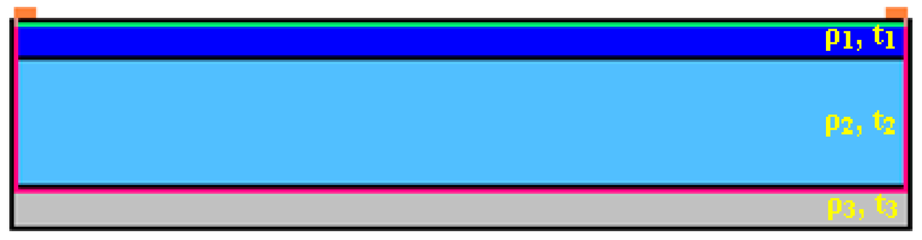
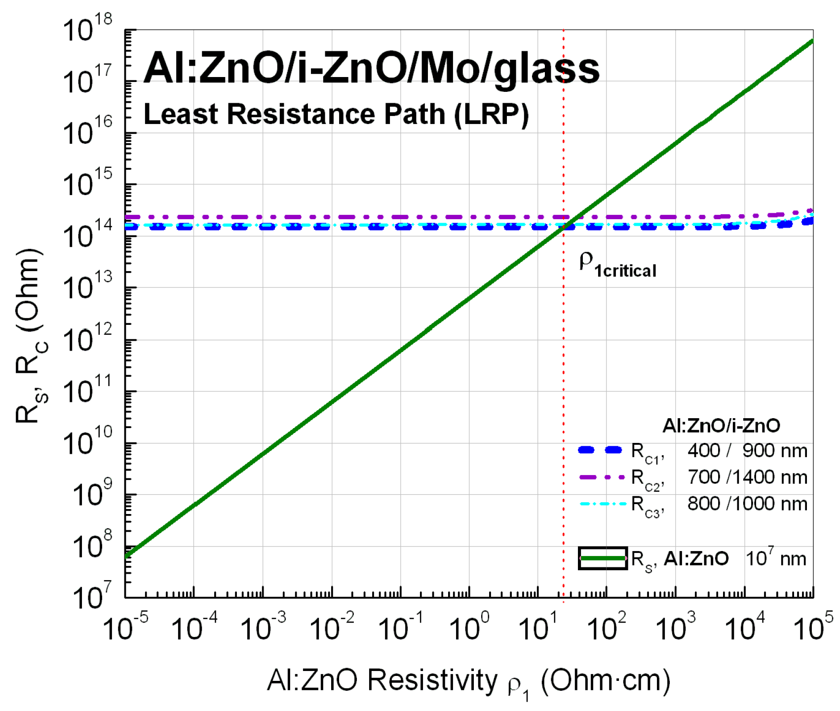
Appendix B.1. Sheet Resistance Measurements/Bulk Resistivity Calculations

The path of least resistance of a thin film sample on glass substrate of square face (L = W = 1 cm) and 3 sub-layers of thickness ti and resistivity ρi (i = 1, 2, 3), with two metal contacts at two adjacent vertices of the uppermost layer (ρ1, t1), is, under the assumption ρ2 > ρ1, ρ3 and t1t3, either a straight line between the two contacts, denoted as s-path (RS), or a straight line running across the top of layer 3 (ρ3, t3) plus two straight lines of micrometric dimensions through layer 2 (ρ2, t2), denoted as c-path (RC) in Figure B1. Both, the s- and c-path, are represented by a square-intersectioned wire of edge d.
The resistances RS and RC as functions of variable resistivity ρ1 are:
R S ( ρ 1 ) = ρ 1 L d 2
R C ( ρ 1 ) = ρ 1 2 t 1 d 2 + ρ 2 2 t 2 d 2 + ρ 3 L d 2
The s-path becomes the preferential least resistance path (LRP) for values of ρ1 lower than a critical value ρ1critical corresponding to RS = RC.
Figure B1. The s-path (green line parallel to Al:ZnO surface) and the c-path (red line normal to Al:ZnO/i-ZnO and parallel to Mo surface).
Energies 09 00951 g009
For 2t1 << L, as in the present case:
ρ 1 c r i t i c a l = ρ 2 2 t 2 L + ρ 3
RS1), RC11), RC21), RC31), and ρ1critical are plotted in Figure B2 using values applying to the cases of the Al:ZnO/i-ZnO on Mo/glass layer deposited by ECD from solutions with 3, 9, and 15 mM AlCl3 solute dopant designated C1, C2, and C3, respectively, in Table B1:
Table B1. Layer type, dimensions, and electrical resistivity.
LayerC1C2C3Resistivity
Al:ZnOt1 = 400 nm700 nm800 nmρ1: variable
i-ZnO t2 = 900 nm1400 nm1000 nmρ2 = 1.33 × 10⁵ Ω·cm
Mot3 = 400 nm400 nm400 nmρ3 = 0.58 × 10⁻⁴ Ω·cm
L = 1 × 10⁷ nm, d = 4 nm.
Figure B2. LRP determination by comparison of RS (solid line) and RC1 (dashed line), RC2 (dash-dot-dot), RC3 (dash-dot) for s-path in Al:ZnO and c-paths in Al:ZnO/i-ZnO/Mo layers; ρ1critical = 23.94 Ω·cm
Energies 09 00951 g010
For values lower than ρ1critical, the measured resistance is dominated by the top current flow; most of the charge carriers use paths through layer 1 and the resistivity of layer 1 can thus be approximately calculated using the experimental data as:
ρ 1 = R m e a s u r e d t 1
where Rmeasured = Vmeasured/Imeasured in 2-point measurements and Rmeasured = Rsheet in the van der Pauw and generally 4-point measurement techniques.

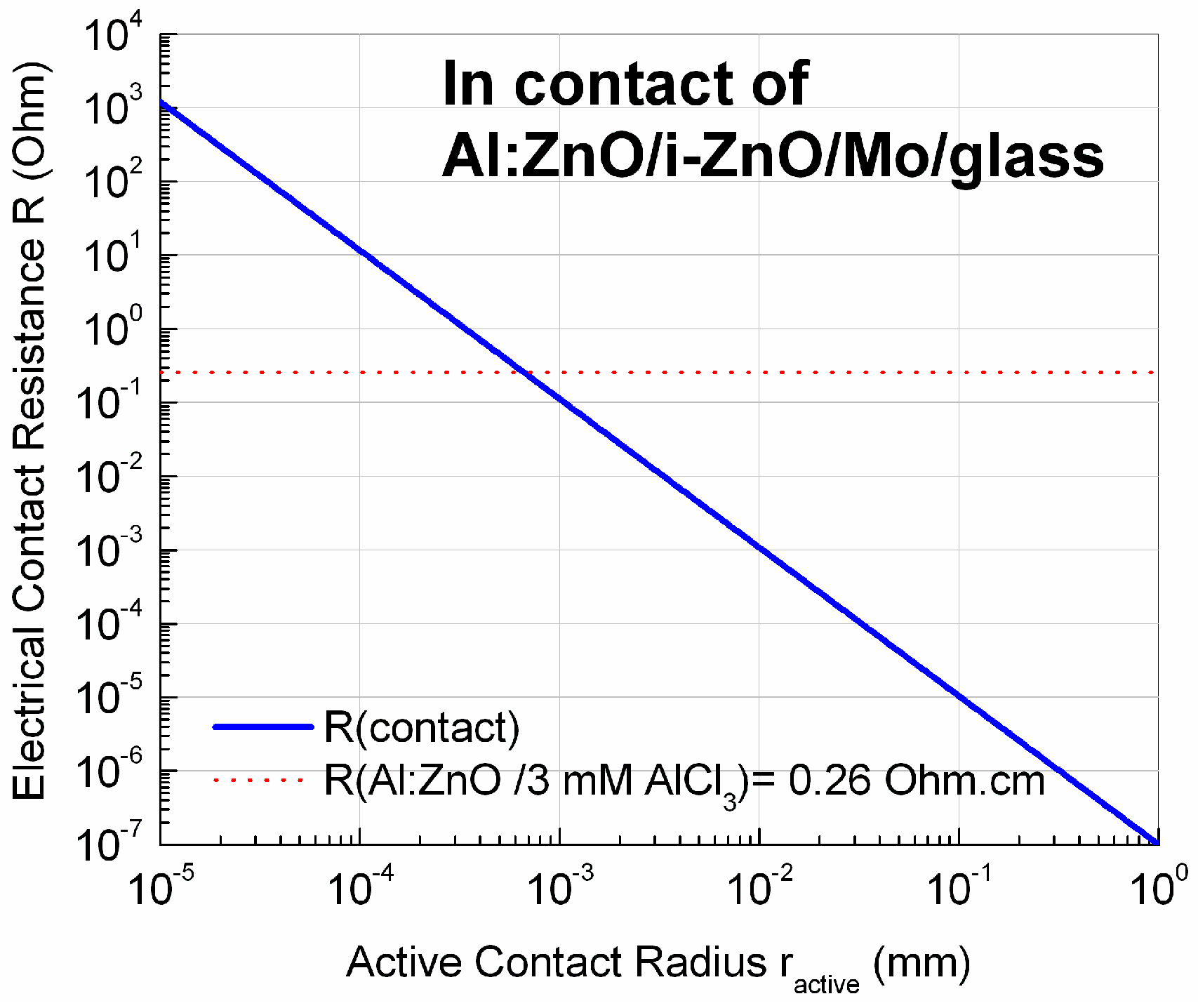
Appendix B.2. Electrical Contact Resistance (ECR)

A general electrical contact resistance theory for conductive rough surfaces was derived from first principles in [91]; a general relation was introduced between the dimensionless real contact area (A*) and the dimensionless ECR (R*) that depends only on the electron mean free path (λ*) as follows:
A * = f 1 ( λ * ) R * f 2 ( λ * )
The dimensionless ECR is thus, in this case, given by:
R * = ( A * f 1 ( λ * ) ) 1 f 2 ( λ * )
with
A * = A a c t i v e / A g e o m
the fraction of the real contact area ( A a c t i v e = π r a c t i v e 2 ) with respect to the apparent area, e.g., the area defined by the contact geometry ( A g e o m = π r g e o m 2 ),
R * = R ( ρ 1 + ρ 2 ) / A g e o m 1 / 2
the contact resistance normalized to the sum of the contact (ρ1) and the contacted layer surface (ρ2) resistivities within the contact area (Ageom),
λ * = λ A g e o m 1 / 2
the electron mean free path λ normalized to the length dimension of the (geometrical) contact area, and f1 and f2 functions of λ*:
f 1 ( λ * ) = a 11 + a 12 λ * ,   a 11 = 2.04 × 10 3 ,   a 12 = 0.435 ;
f 2 ( λ * ) = a 21 + a 22 λ * ,   a 21 = 0.992 ,   a 22 = 1.157 × 10 3 .
In accordance with Equation (B6), the ECR of In-pellet contacted Al:ZnO/i-ZnO/Mo/glass with: ρ1(In) = 8.8 × 10⁻⁶ Ω·cm, ρ2(Al:ZnO) = 1.0 × 10⁻⁵ Ω·cm, rgeom = 0.5 mm, λ(In) = 8.16 nm is plotted in dependence of the radius ractive of the real contact area R(ractive) in Figure B3. If the active contact radius is reduced to the micrometer range, it is apparent that the ECR of the In contact becomes of order 10−1 Ω and interferes with the resistance of the highly doped Al:ZnO layer.
Figure B3. Dependence of the resistance of the In contact on contact radius (solid line); the sheet resistance of the Al:ZnO layer doped with 3 mM AlCl3 solute dopant is also indicated (dotted line).
Energies 09 00951 g011

References

  1. Rau, U.; Schock, H.W. Cu(In,Ga)Se2 solar cells. In Clean Energy from Photovoltaics; Archer, D., Hill, R., Eds.; Imperial College Press: London, UK, 2001; pp. 277–345. [Google Scholar]
  2. Ramanathan, K.; Contreras, M.A.; Perkins, C.L.; Asher, S.; Hasoon, F.S.; Keane, J.; Young, D.; Romero, M.; Metzg, W.; Noufi, R.; et al. Properties of 19.2% Efficiency ZnO/CdS/CuInGaSe2 Thin-film Solar Cells. Prog. Photovolt. Res. Appl. 2003, 11, 225–230. [Google Scholar] [CrossRef]
  3. Repins, I.; Contreras, M.A.; Egaas, B.; DeHart, C.; Scharf, J.; Perkins, C.L.; To, B.; Noufi, R. 19.9%-efficient ZnO/CdS/CuInGaSe2 Solar Cell with 81.2% Fill Factor. Prog. Photovolt. Res. Appl. 2008, 16, 235–239. [Google Scholar] [CrossRef]
  4. Jackson, P.; Hariskos, D.; Lotter, E.; Paetel, S.; Wuerz, R.; Menner, R.; Wischmann, W.; Powalla, M. New world record efficiency for Cu(In,Ga)Se2 thin-film solar cells beyond 20%. Prog. Photovolt. Res. Appl. 2011. [Google Scholar] [CrossRef]
  5. Savadogo, O. Chemically and electrochemically deposited thin films for solar energy materials. Sol. Energy Mater. Sol. Cells 1998, 52, 361–388. [Google Scholar] [CrossRef]
  6. Lincot, D. Electrodeposition of semiconductors. Thin Solid Films 2005, 487, 40–48. [Google Scholar] [CrossRef]
  7. Fauchais, P. Understanding plasma spraying. J. Phys. D Appl. Phys. 2004, 37, R86–R108. [Google Scholar] [CrossRef]
  8. Yoshida, T. Toward a new era of plasma spray processing. Pure Appl. Chem. 2006, 78, 1093–1107. [Google Scholar] [CrossRef]
  9. Azimi, H.; Hou, Y.; Brabec, C.J. Towards low-cost, environmentally friendly printed chalcopyrite and kesterite solar cells. Energy Environ. Sci. 2014, 7, 1829–1849. [Google Scholar] [CrossRef]
  10. Xin, H.; Katahara, J.K.; Braly, I.L.; Hillhouse, H.W. 8% Efficient Cu2ZnSn(S,Se)4 Solar Cells from Redox Equilibrated Simple Precursors in DMSO. Adv. Energy Mater. 2014, 4, 1301823. [Google Scholar] [CrossRef]
  11. Werner, M.; Sutter-Fella, C.M.; Romanyuk, Y.E.; Tiwari, A.N. 8.3% efficient Cu2ZnSn(S,Se)4 solar cells processed from sodium-containing solution precursors in a closed reactor. Thin Solid Films 2015, 582, 308–312. [Google Scholar] [CrossRef]
  12. Lin, X.; Kavalakkatt, J.; Ennaoui, A.; Lux-Steiner, M.-C. Cu2ZnSn(S,Se)4 thin film absorbers based on ZnS, SnS and Cu3SnS4 nanoparticle inks: Enhanced solar cells performance by using a two-step annealing process. Sol. Energy Mater. Sol. Cells 2015, 132, 221–229. [Google Scholar] [CrossRef]
  13. Klenk, R. Characterisation and modelling of chalcopyrite solar cells. Thin Solid Films 2001, 387, 135–140. [Google Scholar] [CrossRef]
  14. Ellmer, K.; Klein, A. ZnO and Its Applications. In Transparent Conductive Zinc Oxide: Basics and Applications in Thin Film Solar Cells; Ellmer, K., Klein, A., Rech, B., Eds.; Springer Series in Materials Science; Springer: Berlin/Heidelberg, Germany, 2007; pp. 1–33. [Google Scholar]
  15. Hariskos, D.; Spiering, S.; Powalla, M. Buffer layers in Cu(In,Ga)Se2 solar cells and modules. Thin Solid Films 2005, 480–481, 99–109. [Google Scholar] [CrossRef]
  16. Fischer, C.; Allsop, N.A.; Gledhill, S.E.; Köhler, T.; Krüger, M.; Sáez-Araoz, R.; Fu, Y.; Schwieger, R.; Richter, J.; Wohlfart, P.; et al. The spray-ILGARs (ion layer gas reaction) method for the deposition of thin semiconductor layers: Process and applications for thin film solar cells. Sol. Energy Mater. Sol. Cells 2011, 95, 1518–1526. [Google Scholar] [CrossRef]
  17. Sáez-Araoz, R.; Krammer, J.; Harndt, S.; Koehler, T.; Krueger, M.; Pistor, P.; Jasenek, A.; Hergert, F.; Lux-Steiner, M.-C.; Fischer, C.-H. ILGAR In2S3 buffer layers for Cd-free Cu(In,Ga)(S,Se)2 solar cells with certified efficiencies above 16%. Prog. Photovolt. Res. Appl. 2012, 20, 855–861. [Google Scholar] [CrossRef]
  18. Wang, L.; Lin, X.; Ennaoui, A.; Wolf, C.; Lux-Steiner, M.-C.; Klenk, R. Solution-processed In2S3 buffer layer for chalcopyrite thin film solar cells. EPJ Photovolt. 2016, 7, 70303. [Google Scholar] [CrossRef]
  19. Papadimitriou, D.; Roupakas, G.; Chatzitheodoridis, E.; Halampalakis, G.; Tselepis, S.; Sáez-Araoz, R.; Lux-Steiner, M.-C.; Nickel, N.H.; Alamé, S.; Vogt, P.; et al. Chemical and Electrochemical Processing of High Quality CIS/CIGS Absorber, Buffer, Window, and Anti-Reflective Coating for Low Cost Photovoltaic Technology. In Proceedings of the 29th European Photovoltaic Solar Energy Conference and Exhibition, PVSEC, Amsterdam, The Netherlands, 22–26 September 2014; pp. 1812–1815.
  20. Papadimitriou, D.; Roupakas, G.; Sáez-Araoz, R.; Lux-Steiner, M.-C.; Nickel, N.H.; Alamé, S.; Vogt, P.; Kneissl, M. Quality CuInSe2 and Cu(In,Ga)Se2 thin films processed by single step electrochemical deposition techniques. Mater. Res. Express 2015, 2, 1–15. [Google Scholar] [CrossRef]
  21. Papadimitriou, D.N. Structural, optical, electrical properties, and strain/stress of electrochemically deposited highly doped ZnO layers and nanostructured ZnO antireflective coatings for cost-effective photovoltaic device technology. Thin Solid Films 2016, 605, 215–231. [Google Scholar] [CrossRef]
  22. Ohm, W.; Riedel, W.; Askünger, Ü.; Heinemann, M.D.; Kaufmann, C.; Garzia, J.L.; Izqierdo, V.; Fontane, X.; Goislard, T.; Lux-Steiner, M.-C.; et al. An overview of technological aspects of Cu(In,Ga)Se2 solar cell architectures incorporating ZnO nanorod arrays. Phys. Status Solidi A 2015, 212, 76–87. [Google Scholar] [CrossRef]
  23. Wei, S.H.; Zhang, S.B.; Zunger, A. Effects of Ga addition to CuInSe2 on its electronic, structural, and defect properties. Appl. Phys. Lett. 1998, 72, 3199–3201. [Google Scholar] [CrossRef]
  24. Dharmadasa, I.M. Advances in Thin-Film Solar Cells; CRC Press: Boca Raton, FL, USA, 2012; pp. 95–122. [Google Scholar]
  25. Schulmeyer, T.; Kniese, R.; Hunger, R.; Jaegermann, W.; Powalla, M.; Klein, A. Influence of Cu(In,Ga)Se2 band gap on the valence band offset with CdS. Thin Solid Films 2004, 451–452, 420–423. [Google Scholar] [CrossRef]
  26. Theodoropoulou, S.; Papadimitriou, D.; Rega, N.; Siebentritt, S.; Lux-Steiner, M.-C. Raman and photoreflectance study of CuIn1-xGaxSe2 epitaxial layers. Thin Solid Films 2006, 511–512, 690–694. [Google Scholar] [CrossRef]
  27. Theodoropoulou, S.; Papadimitriou, D.; Anestou, K.; Cobet, C.; Esser, N. Optical properties of CuIn1−xGaxSe2 quaternary alloys for solar-energy conversion. Semicond. Sci. Technol. 2009, 24, 1–8. [Google Scholar] [CrossRef]
  28. Kaufmann, C.A.; Caballero, R.; Unold, T.; Hesse, R.; Klenk, R.; Schorr, S.; Nichterwitz, M.; Schock, H.-W. Depth profiling of Cu(In,Ga)Se2 thin films grown at low temperatures. Sol. Energy Mater. Sol. Cells 2009, 93, 859–863. [Google Scholar] [CrossRef]
  29. Caballero, R.; Kaufmann, C.A.; Efimova, V.; Rissom, T.; Hoffmann, V.; Schock, H.-W. Investigation of Cu(In,Ga)Se2 thin-film formation during the multi-stage co-evaporation process. Prog. Photovolt. Res. Appl. 2013, 21, 30–46. [Google Scholar] [CrossRef]
  30. Fons, P.; Niki, S.; Uchino, M.; Yamaa, A.; Ouangi, H. A High Resolution X-ray Diffraction and TEM Study of the CuxSe Surface Phase of Cu-rich CuInSe2. Jpn. J. Appl. Phys. 2000, 39, 189–191. [Google Scholar] [CrossRef]
  31. Papadimitriou, D. Application of optical spectroscopic techniques in the characterization of elastic strain effects in semiconductor heterostructures and nanostructures and in semiconductor-based thin-film solar cells. Phys. Status Solidi B 2015, 252, 30–55. [Google Scholar] [CrossRef]
  32. Xue, C.; Papadimitriou, D.; Esser, N. Optical characterization of epitaxial CuxGaySe2-layers by photoreflectance spectroscopy. Thin Solid Films 2004, 451–452, 189–192. [Google Scholar] [CrossRef]
  33. Papadimitriou, D.; Esser, N.; Xue, C. Structural properties of chalcopyrite thin films studied by Raman spectroscopy. Phys. Status Sol. 2005, 242, 2633–2643. [Google Scholar] [CrossRef]
  34. Tanino, H.; Maeda, T.; Fujikake, H.; Nakanishi, H.; Endo, S.; Irie, T. Raman spectra of CuInSe2. Phys. Rev. B 1992, 45, 13323–13330. [Google Scholar] [CrossRef]
  35. Ohrendorf, F.W.; Haeuseler, H. Lattice Dynamics of Chalcopyrite Type Compounds. Part I. Vibrational Frequencies. Cryst. Res. Technol. 1999, 34, 339–349. [Google Scholar] [CrossRef]
  36. Xue, C.; Papadimitriou, D.; Raptis, Y.S.; Richter, W.; Esser, N.; Siebentritt, S.; Lux-Steiner, M.Ch. Micro-Raman Study of Orientation Effects of CuxSe-Crystallites on Cu-rich CuGaSe2 Thin Films. J. Appl. Phys. 2004, 96, 1963–1966. [Google Scholar] [CrossRef]
  37. Joint Committee on Powder Diffraction Standards—International Centre for Diffraction Data; JCPDS-ICDD: Newtown Square, PA, USA, 1950–2000; Card number: CuInSe2 (40–1487), CuIn70Ga30Se2 (35-1102), Cu2Se (27–1131, 37–1187), Cu2-xSe (71–0044), ZnO (36–1451), ZnSe hexagonal (15-0105), ZnSe cubic (37–1463), Mo (42–1120), MoSe2 (29-0914, 01–077–1715).
  38. Siebentritt, S. Wide gap chalcopyrites: Material properties and solar cells. Thin Solid Films 2002, 403–404, 1–8. [Google Scholar] [CrossRef]
  39. Wei, S.-H.; Zunger, A. Band offsets at the CdS/CuInSe2 heterojunction. Appl. Phys. Lett. 1993, 63, 2549–2551. [Google Scholar] [CrossRef]
  40. Schmid, D.; Ruckh, M.; Schock, H.W. Photoemission studies on Cu(In,Ga)Se2 thin films and related binary selenides. Appl. Surf. Sci. 1996, 103, 409–429. [Google Scholar] [CrossRef]
  41. Rau, U.; Schmidt, M. Electronic properties of ZnO/CdS/Cu(In,Ga)Se2 solar cells-aspects of heterojunction formation. Thin Solid Films 2001, 387, 141–146. [Google Scholar] [CrossRef]
  42. Hofmann, A.; Pettenkofer, C. Surface orientation dependent band alignment for CuInSe2–ZnSe–ZnO. Appl. Phys. Lett. 2011, 98, 113503. [Google Scholar] [CrossRef]
  43. Fearheiley, M.L.; Bachmann, K.J.; Shing, Y.-H.; Vasquez, S.A.; Herrington, C.R. The Lattice Constants of CulnSe2. J. Electron. Mater. 1985, 14, 677–683. [Google Scholar] [CrossRef]
  44. Fiedeler, U. Rekombination und Diffusion in CuGaSe2—Solarzellen: Photolumineszenz und Quanteneffizienzuntersuchungen an MOCVD Gewachsenen Absorbern. Ph.D. Thesis, Freie Universität Berlin, Berlin, Germany, 2002. [Google Scholar]
  45. Fuertes-Marrón, D. Structural and Electronic Characterisation of Thin-Film Solar Cells Based on CVD-Grown CuGaSe2. Ph.D. Thesis, Freie Universität Berlin, Berlin, Germany, 2003. [Google Scholar]
  46. Rega, N. Photolumineszenz von Epitaktischen Cu(In,Ga)Se2-Schichten. Ph.D. Thesis, Freie Universität Berlin, Berlin, Germany, 2004. [Google Scholar]
  47. Riha, S.C.; Johnson, D.C.; Prieto, A.L. Cu2Se Nanoparticles with Tunable Electronic Properties Due to a Controlled Solid-State Phase Transition Driven by Copper Oxidation and Cationic Conduction. J. Am. Chem. Soc. 2011, 133, 1383–1390. [Google Scholar] [CrossRef] [PubMed]
  48. Tyagi, K.; Gahtori, B.; Bathula, S.; Jayasimhadri, M.; Singh, N.-K.; Sharma, S.; Haranath, D.; Srivastava, A.K.; Dhar, A. Enhanced thermoelectric performance of spark plasma sintered copper-deficient nanostructured copper selenide. J. Phys. Chem. Solids 2015, 81, 100–105. [Google Scholar] [CrossRef]
  49. Gabor, A.M.; Tuttle, J.R.; Albin, D.S.; Contreras, M.A.; Noufi, R.; Hermann, A.M. High-efficiency CuIn1-xGaxSe2 solar cells made from (Inx,Ga1-x)2Se3 precursor films. Appl. Phys. Lett. 1994, 65, 198–200. [Google Scholar] [CrossRef]
  50. Cullity, B.D. Elements of X-Ray Diffraction; Addison-Wesley: Reading, MA, USA, 1978. [Google Scholar]
  51. Kolb, E.D.; Laudise, R.A. Hydrothermal Crystallization of Zinc Selenide. J. Cryst. Growth 1970, 7, 199–202. [Google Scholar] [CrossRef]
  52. Kolb, E.D.; Coriell, A.S.; Laudise, R.A.; Hutson, A.R. The Hydrothermal Growth of Low Carrier Concentration ZnO at High Water and Hydrogen Pressures. Mater. Res. Bull. 1967, 2, 1099–1106. [Google Scholar] [CrossRef]
  53. Laudise, R.A.; Kolb, E.D.; Caporaso, A.J. Hydrothermal Growth of Large Sound Crystals of Zinc Oxide. J. Am. Ceram. Soc. 1964, 47, 9–12. [Google Scholar] [CrossRef]
  54. Hanada, T. Basic Properties of ZnO, GaN, and Related Materials. In Oxide and Nitride Semiconductors: Processing, Properties, and Applications; Yao, T., Hong, S.-K., Eds.; Springer Series; Springer: Berlin/Heidelberg, Germany, 2009; pp. 1–20. [Google Scholar]
  55. Kisielowski, C.; Krüger, J.; Ruvimov, S.; Suski, T.; Ager, J.W., III; Jones, E.; Liliental-Weber, Z.; Rubin, M.; Weber, E.R.; Bremser, M.D.; et al. Strain-related phenomena in GaN thin films. Phys. Rev. B 1996, 54, 17745–17753. [Google Scholar] [CrossRef]
  56. Azuhata, T.; Takesada, M.; Yagi, T.; Shikanai, A.; Chichibu, S.F.; Torii, K.; Nakamura, A.; Sota, T.; Cantwell, G.; Eason, D.B.; et al. Brillouin scattering study of ZnO. J. Appl. Phys. 2003, 94, 968–972. [Google Scholar] [CrossRef]
  57. Rössler, U. ZnO: Bulk Modulus, Compressibility in New Data and Updates for Several Semiconductors with Chalcopyrite Structure, for Several II-VI Compounds, and Diluted Magnetic IV-VI Compounds, Landolt-Börnstein—Group III Condensed Matter; Springer: Berlin/Heidelberg, Germany, 2013; pp. 159–169. [Google Scholar]
  58. Van de Walle, C.G.; Martin, R.M. Theoretical Study of Band Offsets at Semiconductor Interfaces. In Electronic Structure of Semiconductor Heterojunctions; Margaritondo, G., Ed.; Perspectives in Condensed Matter Physics 1; Kluwer Academic Publishers: Dordrecht, The Netherlands, 1988; pp. 268–279. [Google Scholar]
  59. Schlachter, S.I.; Fietz, W.H.; Grube, K.; Goldacker, W. High Pressure Studies of Tc and Lattice Parameters of MgB2, Advances in Cryogenic Engineering. In Proceedings of the International Cryogenic Materials Conference—ICMC, Xi’an, China, 16–20 June 2002; Volume 48, pp. 809–816.
  60. Adachi, S. Properties of Group-IV, III-V and II-VI Semiconductors. John Wiley & Sons: Hoboken, NJ, USA, 2005; p. 45. [Google Scholar]
  61. Berlincourt, D.; Jaffe, H.; Shiozawa, L.R. Electroelastic Properties of the Sulfides, Selenides, and Tellurides of Zinc and Cadmium. Phys. Rev. 1963, 129, 1009. [Google Scholar] [CrossRef]
  62. Klingshirn, C.; Fallert, J.; Zhou, H.; Sartor, J.; Thiele, C.; Maier-Flaig, F.; Schneider, D.; Kalt, H. 65 years of ZnO research—Old and very recent results. Phys. Status Solidi B 2010, 247, 1424–1447. [Google Scholar] [CrossRef]
  63. Özgür, Ü.; Alivov, Y.I.; Liu, C.; Teke, A.; Reshchikov, M.A.; Doğan, S.; Avrutin, V.; Cho, S.-J.; Morkoç, H. A comprehensive review of ZnO materials and devices. J. Appl. Phys. 2005, 98, 041301. [Google Scholar] [CrossRef]
  64. Zhang, Y.; Ram, M.K.; Stefanakos, E.K.; Goswami, D.Y. Synthesis, Characterization, and Applications of ZnO Nanowires. J. Nanomater. 2012. [Google Scholar] [CrossRef]
  65. Park, S.-H.; Seo, S.-Y.; Kim, S.-H.; Han, S.-W. Surface roughness and strain effects on ZnO nanorod growth. Appl. Phys. Lett. 2006, 88, 251903. [Google Scholar] [CrossRef]
  66. Gu, F.; Gai, L.; Shao, W.; Li, C.; Schmidt-Mende, L. Heteroepitaxial growth of ZnO branches selectively on Ti02 nanorod tips with improved light harvesting performance. Chem. Commun. 2011, 47, 8400–8402. [Google Scholar] [CrossRef] [PubMed] [Green Version]
  67. Contreras, M.A.; Jones, K.M.; Gedvilas, L.; Matson, R. Preferred Orientation in Polycrystalline Cu(In,Ga)Se2 and Its Effect on Absorber Thin-Films and Devices. In Proceedings of the 16th European Photovoltaic Solar Energy Conference and Exhibition, Glasgow, UK, 1–5 May 2000.
  68. Kubelka, P.; Munk, F. Ein Beitrag zur Optik der Farbanstriche. Z. Tech. Phys. 1931, 12, 593–601. [Google Scholar]
  69. Sandoval, C.; Kim, A.D. Deriving Kubelka-Munk theory from radiative transport. J. Opt. Soc. Am. A 2014, 31, 628–636. [Google Scholar] [CrossRef] [PubMed]
  70. Tauc, J.; Grigorovici, R.; Vancu, A. Optical Properties and Electronic Structure of Amorphous Germanium. Phys. Status Sol. B 1966, 15, 627–637. [Google Scholar] [CrossRef]
  71. Kröger, F.A. The Chemistry of Imperfect Crystals; North-Holland Pub. Co.: Amsterdam, The Netherlands, 1964. [Google Scholar]
  72. Avadhut, Y.S.; Weber, J.; Hammarberg, E.; Feldmann, C.; der Günne, J.S. Structural investigation of aluminium doped ZnO nanoparticles by solid-state NMR spectroscopy. Phys. Chem. Chem. Phys. 2012, 14, 11610–11625. [Google Scholar] [CrossRef] [PubMed]
  73. Serier, H.; Gaudon, M.; Ménétrier, M. Al-doped ZnO powdered materials: Al solubility limit and IR absorption properties. Solid State Sci. 2009, 11, 1192–1197. [Google Scholar] [CrossRef]
  74. Sanzaro, S.; la Magna, A.; Smecca, E.; Mannino, G.; Pellegrino, G.; Fazio, E.; Neri, F.; Alberti, A. Controlled Al3+ Incorporation in the ZnO Lattice at 188 °C by Soft Reactive Co-Sputtering for Transparent Conductive Oxides. Energies 2016, 9, 433. [Google Scholar] [CrossRef]
  75. Ennaoui, A. High Efficiency CIGSS Thin Film based Solar Cells and Mini-modules. Moroc. J. Condens. Matter 2000, 3, 8–15. [Google Scholar]
  76. Buckley, A.N.; Woods, R. An X-ray photoelectron spectroscopic study of the oxidation of chalcopyrite. Aust. J. Chem. 1984, 37, 2403–2413. [Google Scholar] [CrossRef]
  77. Acres, R.G.; Harmer, S.L.; Beattie, D.A. Synchrotron XPS studies of solution exposed chalcopyrite, bornite, and heterogeneous chalcopyrite with bornite. Int. J. Miner. Process. 2010, 94, 43–51. [Google Scholar] [CrossRef]
  78. Ahmed, E. Growth and Characterization of Cu(In,Ga)Se2 Thin Films for Solar Cell Applications. Ph.D. Thesis, University of Salford, Salford, UK, 1995. [Google Scholar]
  79. Ramanathan, K.; Keane, J.; Noufi, R. Properties of High-Efficiency CIGS Thin-Film Solar Cells. In Proceedings of the 31st IEEE Photovoltaics Specialists Conference and Exhibition, Lake Buena Vista, FL, USA, 3–7 January 2005.
  80. Messmann-Vera, L.-A. Einfluss der Undotierten ZnO-Schicht auf die elektrischen Eigenschaften von ZnO/Cu(In,Ga)Se2-Solarzellen, Master’s Thesis, Technische Universität Berlin, Berlin, Germany, 2010. [Google Scholar]
  81. Desal, P.D.; Chu, T.K.; James, H.M.; Ho, C.Y. Electrical Resistivity of Selected Elements. J. Phys. Chem. Ref. Data 1984, 13, 1069–1096. [Google Scholar]
  82. Scofield, J.H.; Duda, A.; Albin, D.; Ballard, B.L.; Predecki, P.K. Sputtered Molybdenum Bilayer Back Contact for Copper Indium Diselenide-Based Polycrystalline Thin-Film Solar Cells. Thin Solid Films 1995, 260, 26–31. [Google Scholar] [CrossRef]
  83. Chen, S.-F.; Wang, S.-J.; Lee, W.-D.; Chen, M.-H.; Wei, C.-N.; Bor, H.-Y.Y. Preparation and Characterization of Molybdenum Thin Films by Direct-Current Magnetron Sputtering. Atlas J. Mater. Sci. 2015, 2, 54–59. [Google Scholar] [CrossRef]
  84. Ellmer, K.; Bikowski, A. Intrinsic and extrinsic doping of ZnO and ZnO alloys. J. Phys. D Appl. Phys. 2016, 49, 413002. [Google Scholar] [CrossRef]
  85. Ellmer, K. Resistivity of polycrystalline zinc oxide films: Current status and physical limit. J. Phys. D Appl. Phys. 2001, 34, 3097–3108. [Google Scholar] [CrossRef]
  86. Ellmer, K. Electrical Properties. In Transparent Conductive Zinc Oxide Basics and Applications in Thin Film Solar Cells; Ellmer, K., Klein, A., Rech, B., Eds.; Springer Series in Materials Science; Springer: Berlin/Heidelberg, Germany, 2007; Volume 104, pp. 35–78. [Google Scholar]
  87. Denhoff, M.W. An accurate calculation of spreading resistance. J. Phys. D Appl. Phys. 2006, 39, 1761–1765. [Google Scholar] [CrossRef]
  88. Berger, H.H. Contact Resistance and Contact Resistivity. J. Electrochem. Soc. 1972, 119, 507–514. [Google Scholar] [CrossRef]
  89. Marlow, G.S.; Das, M.B. The Effects of Contact Size and non-zero Metal Resistance on the Determination of Specific Contact Resistance. Solid State Electron. 1982, 25, 91–94. [Google Scholar] [CrossRef]
  90. Gall, D. Electron mean free path in elemental metals. J. Appl. Phys. 2016, 119, 085101. [Google Scholar] [CrossRef]
  91. Kogut, L.; Komvopoulos, K. Electrical contact resistance theory for conductive rough surfaces. J. Appl. Phys. 2003, 94, 3153–3162. [Google Scholar] [CrossRef]
  92. Ellmer, K.; Diesner, K.; Wendt, R.; Fiechter, S. Relations between Texture and Electrical Parameters of Thin Polycrystalline Zinc Oxide Films. Solid State Phenom. 1996, 51–52, 541–546. [Google Scholar] [CrossRef]
  93. Cebulla, R.; Wendt, R.; Ellmer, K. Al-Doped Zinc Oxide Films Deposited by Simultaneous RF and DC Excitation of a Magnetron Plasma: Relationships between Plasma Parameters and Structural and Electrical Film Properties. J. Appl. Phys. 1998, 83, 1087–1095. [Google Scholar] [CrossRef]
  94. Lee, C.; Lim, K.; Song, J. Highly textured ZnO thin films doped with indium prepared by the pyrosol method. Sol. Energy Mater. Sol. Cells 1996, 43, 37–45. [Google Scholar] [CrossRef]
Figure 1. CuIn70Ga30Se2 solar absorber in dependence of KCN etch-time: images of (a) untreated surface and (b,c) surfaces etched 3 and 7 min, respectively, as viewed with the optical microscope coupled to the micro-Raman spectrometer; (d) Raman spectra; and (e) frequencies, widths (FWHM), and integrated intensities of Raman modes at 177.9 cm−1 (A1, circles), 224.2 cm−1 (B12, up-triangles), and 256.3 cm−1 (B2, down-triangles) in dependence of etching time (lines are guide to the eye).
Energies 09 00951 g001
Figure 2. X-ray diffractograms of (a) CuIn70Ga30Se2 solar absorber on Mo/glass substrate and (b) Al:ZnO/ZnSe/CuIn70Ga30Se2/Mo/glass solar structures annealed sequentially in two steps: 1st-step: 350 °C, 2 h, N2-flow (TFS-I_1, thick-solid line) and 2nd-step: 400 °C, 2 h, N2-purge (TFS-I_2, thin-solid line).
Energies 09 00951 g002
Figure 3. Bragg-reflections of Al:ZnO on ZnSe/CuIn70Ga30Se2/Mo/glass thin film structure TFS-II subjected to 2-step annealing procedure (TFS-II_1 and TFS-II_2): (a) Al:ZnO (100), 2θ = 33.68°, Γ = 0.41° and Al:ZnO (002), 2θ = 36.05°, Γ = 0.61°; and (b) Al:ZnO (101), 2θ = 38.04°, Γ = 0.24° of TFS-II_2 fitted with Lorentzians (dashed-lines) in accordance with the contributions of the CIGS/Mo/glass substrate and an Al:ZnO reference layer on i-ZnO/Mo/glass doped with 9 mM AlCl3 solute dopant.
Energies 09 00951 g003
Figure 4. Scanning electron microscopy images of Al:ZnO bilayer on ZnSe/Cu(In,Ga)Se2/Mo/glass: (a) top-view (inset: e-gun focus at 100 μm) and (b) cross-sectional view (layer thickness: Al:ZnO = 1.2 μm, CIGS = 2.4 μm, Mo = 0.4 μm).
Energies 09 00951 g004
Figure 5. Al:ZnO/ZnO test structures on Mo/glass: (a) Reflectance spectra in the NUV-VIS region and (b) tauc-plots in dependence of the AlCl3 solute dopant concentration of the ECD process.
Energies 09 00951 g005
Figure 6. Al:ZnO/ZnO test structures: (a) Band-gap energy in dependence of AlCl3 solute dopant concentration and the respective [Al] at. % incorporated in the ZnO lattice [21] and (b) hydrostatic strain of Al:ZnO versus [Al] at. %.
Energies 09 00951 g006
Figure 7. Al:ZnO bilayer on solar ZnSe/CuIn70Ga30Se2/Mo/glass thin film structures (TFS-I & TFS-II) annealed in two steps, 1st-step: 350 °C, 2 h, N2-flow (TFS-I_1 & TFS-II_1) and 2nd-step: 400 °C, 2 h, N2-purge (TFS-I_2 & TFS-II_2): (a) tauc-plots of CIGS absorber (in the inset: TFS spectral reflectance) and (b) tauc-plots of Al:ZnO window bilayer.
Energies 09 00951 g007
Figure 8. Resistivity (Ω·cm) of ECD processed highly doped Al:ZnO sheets on i-ZnO/Mo/glass in dependence of AlCl3 solute dopant concentration (full circles); for comparison, the resistivity of the molybdenum thin film (square) on glass substrate is also plotted.
Energies 09 00951 g008

