1. Introduction
Stable table high quality hydrogenated microcrystalline silicon (μc-Si:H) films which are used in thin-film silicon tandem solar cells have been difficult to make since the quality of μc-Si:H varies depending on its underlying shape or film thickness [
1]. This is because a defective component in the μc-Si:H film is affected by transparent conductive oxide (TCO) texture, as the film thickness of the microcrystalline silicon increases [
2]. To avoid a defective region being formed and achieve high conversion efficiency (
Eff), the surface morphology of TCO was modified to have a blunt angle or rounded shape [
3]. Recently, École Polytechnique Fédérale de Lausanne has developed thin-film silicon solar cells with 12.63% efficiency [
4]. Also, as the current maximum value of
Eff, the National Institute of Advanced Industrial Science and Technology (AIST) reported the
Eff of 12.69% with a triode plasma-enhanced chemical vapor deposition (PECVD) reactor [
5].
As a model of a defective region generated, when μc-Si:H is grown from the slope of the texture shape of TCO, a defective region ingenerates at the collided point of each μc-Si:H [
6,
7]. A defective region is affected by the underlying shape or the underlying film quality. It has been reported that the defective region consists of vacancies and a low-density amorphous region [
2]. Previously, we proposed another factor for the formation of a defective region due to the shadowing effect on incident radicals [
2], which should reduce the
Xc [
8].
Beyond that, a defective region also occurs with the continuous deposition film after becoming thicker. This defect region was caused by colliding with the neighboring grains after the film become thicker [
9]. This is because μc-Si:H grows perpendicular to the textured substrate. The reduction in
Xc was revealed by micro-crystallinity depth profiling measurements [
8,
10]. An
Xc profiling technique was reported by Choong
et al. who measured the
Xc profiling of the early-stage (<800 nm) of μc-Si:H. Therefore, in this report, we aim to reduce the collisions with the neighboring grains by stopping the PECVD once to make the epitaxial μc-Si:H film thinner (>1000 nm). Finally, a high conversion efficiency solar cell can be expected. Since the beginning period of discharge is an unstable process, the value of
Xc can be expected to decrease if epitaxial growth of μc-Si:H is halted by temporarily stopping the PECVD. Impurities which come from the deposition chamber also influence the quality of μc-Si:H.
As a comparative experiment to reduce the defective region correlating to the film thickness gain, an experiment was carried out. The experimental method is very simple; the plasma-discharge of very high frequency (VHF) PECVD should be stopped once and then the chamber with a vacuum is held for a few seconds (although this process stopped the epitaxial growth of μc-Si:H, this experimental method is referred to as “
SEG”). In the actual experiment,
SEG, which was done twice or three times, produces an equal thickness during the i-layer deposition. For ease of evaluating
SEG, all samples were deposited with pulsed-PECVD [
11]. This is because the pulsed-PECVD can be expected to reduce the ion-bombardment and short lifetime species [
12,
13]. Using a different
SEG method, characteristic improvement was reported by Urbain
et al. [
14]. Even though they used a different way of profiling the controlled SiH
4, the aim of suppressing the reduction of
Xc was the same as that of the
SEG experiments. In only the experiment where
SEG was done twice using the thin-film silicon tandem solar cells, this
Xc of test cells became higher than that of normal-condition cells, and it did not decrease during the process of forming a thick film as well as the case using
Xc-adjustment layer [
8]. Eventually,
Eff improved by 1.3% (0.14 points),
Voc by 0.011 V, and
FF by 0.002 compared with those for the normal-condition cell.
2. Experimental Methods
In this study, actual thin-film silicon tandem solar cells were used for the evaluation of
SEG. The structure of these cells was glass/tin oxide (SnO
2)/a-Si:H (p-i-n)/µc-Si:H (p-i-n)/back electrode [
15]. For TCO, a commercial SnO
2-based TCO substrate (Asahi VU, Asahi Glass, Tokyo, Japan) was adopted. μc-Si:H and a-Si:H were deposited by plasma-enhanced chemical vapor deposition (PECVD).
Typically, when the μc-Si:H is deposited with PECVD, the plasma-discharge power is not stopped before reaching the target thickness. However, in this study, when the thickness reached one-third of t (t/3) and two-thirds of t (2t/3),
SEG was done twice, if the total thickness of i-µc-Si:H is t (=2300 nm). The evacuation times of
SEG were carried out in two modes: 30 s and 600 s, and these were labeled cells A and B, respectively. This degree of vacuum was under 5 × 10
−3 (pa). The vacuum time of 30 s was determined by the time required for the deposition gases (SiH
4/H
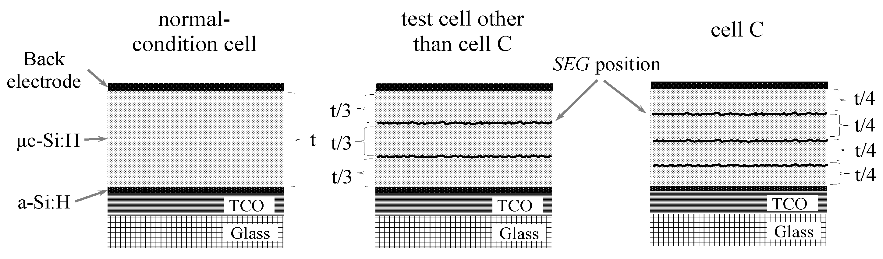
2) to me almost completely eliminated from the chamber. It is due to a return to the default deposition position. The impact of long time exposure of the cell to the vacuum chamber was compared with that for the cell with the 600 s exhaust time (B cells). Only the difference between cell A and cell B influences the impurities while discharge is halted. The structures of a normal-condition cell and a cell made using the
SEG cell (cells A and B) are shown in
Figure 1.
Additionally, different numbers of
SEG experiments were carried out simultaneously. Since
Xc is correlated with the film thickness, the value of
Xc changes according to the number of
SEG. When the thickness reached one-fourth of t (t/4), two-fourths of t (2t/4), and three-fourths of t (3t/4),
SEG was done three times, if the total thickness of i-µc-Si:H is t (=2300 nm). One evacuation time of
SEG was 30 s, which is the same as for cell A. This was labeled cell C. The degree of vacuum was under 5 × 10
−3 (pa), which is the same as for cells A and B.
Table 1 summarizes these conditions.
Figure 1.
Cell structure comparison between normal-condition, SEG (other than cell C) and a SEG cell (cell C). The i-μc-Si:H thicknesses were t. SEG was done when the thicknesses reached t/3 and 2t/3, t/4, 2t/4, and 3t/4.
Figure 1.
Cell structure comparison between normal-condition, SEG (other than cell C) and a SEG cell (cell C). The i-μc-Si:H thicknesses were t. SEG was done when the thicknesses reached t/3 and 2t/3, t/4, 2t/4, and 3t/4.
Table 1.
Comparison of i-μc-Si:H thickness constitution with normal-condition cells A, B and C; as well as normal-condition film and films A. One time of evacuations times of SEG, and total evacuations times of that with films A and cells A, B and C.
Table 1.
Comparison of i-μc-Si:H thickness constitution with normal-condition cells A, B and C; as well as normal-condition film and films A. One time of evacuations times of SEG, and total evacuations times of that with films A and cells A, B and C.
| Description | Normal Condition Cell/Film | Cell A/Film A | Cell B | Cell C |
|---|
| i-layer constitution | t | t/3 + t/3 + t/3 | t/4 + t/4 + t/4 + t/4 |
| total i-later thickness | t (=2300 nm) |
| exhaust time between i-layer (s) | 0 | 30 | 600 | 30 |
| total exhaust time (s) | 0 | 60 | 1200 | 90 |
The cell position and temperature of the heater were maintained during SEG. After the SEG, the same gases as the deposition conditions were supplied for 30 s, and then plasma-dischargewas restarted again. The total discharge time of μc-Si:H was the same for the whole duration of these experiments, although the discharge was stopped during the deposition. All the μc-Si:H treatment times with PECVD became longer by only around 5 min, except for cell B.
Furthermore, to verify the reproducibility of the
SEG process, two other types of
SEG tests were carried out. These test conditions were different from the conditions applied to cells A to C, such as the top layer and i-μc-Si:H. However, the
SEG processes were carried out twice, the same as for cell A. The total thicknesses of i-μc-Si:H were 1500 and 1750 nm: these were labeled cells D and E, respectively. For cell D, the deposition conditions (thickness, gases, power and pressure) of i-μc-Si:H and the top layer condition were varied compared to other cells. Cell E was subjected to conditions different from those applied to cells A to D. The no-
SEG cells were fabricated simultaneously, and were labeled as having been fabricated under the same normal conditions as those for cell D and cell E.
Table 2 summarizes these conditions.
Table 2.
Comparison of different i-μc-Si:H thickness (1500/1750 nm) SEG processes with cell D and normal-condition cell D, and cell E and normal-condition cell E. Single evacuation times of SEG and total exhaust time of cell.
Table 2.
Comparison of different i-μc-Si:H thickness (1500/1750 nm) SEG processes with cell D and normal-condition cell D, and cell E and normal-condition cell E. Single evacuation times of SEG and total exhaust time of cell.
| Description | Normal Condition (D) | Cell D | Normal Condition (E) | Cell E |
|---|
| i-layer constitution | t | t/3 + t/3 + t/3 | t | t/3 + t/3 + t/3 |
| total i-later thickness | t (=1500 nm) | t (=1750 nm) |
| exhaust time between i-layer (s) | 0 | 30 | 0 | 30 |
| tolal exhaust time (s) | 0 | 60 | 0 | 60 |
The thickness of the i-layer (a-Si:H) in the top layer was sufficient at 240 nm. This was to ensure that the top layer current would have no effect on the bottom layer current, since the bottom layer current has a rate-controlling effect on Isc.
For each condition test, five to eight cells were fabricated. The active area of each cell was 1 cm2. The I–V characteristics of open circuit voltage (Voc), short circuit current (Isc), fill factor (FF), and conversion efficiency (Eff) were measured using a solar simulator under an air mass of 1.5 (AM 1.5) at 25 °C.
Pulsed PECVD was used at all times during the i-µc-Si:H process. As the pulsed PECVD conditions, a PECVD frequency of 40 MHz, a pulse modulation frequency of 30 kHz, and a duty ratio of 50% were adopted for i-layer deposition.
For the comparison of
Xc, actual normal-condition and cell A cells were used in the analysis with a polishing method. This method was reported in [
8]. The actual cell A was analyzed by secondary ion mass spectrometry (SIMS) [
16]. Nitrogen and oxygen were analyzed through to the glass substrate from the back electrode side of the cell. SIMS measurementing conditions were as follows: Equipment: CAMECA ims5f (CAMECA, Gennevilliers Cedex, France) Ion conditions: Cs+, 14.5 keV, approximately 30 nA; Measuring area: approximately 30 μm diameter; Depth: calibration by Si sputtering.
In addition to the evaluation of cells, μc-Si:H films have been analyzed simultaneously. In the film evaluations, Eagle XG (Corning, NY, USA) was used as the substrate. A 20 nm p-layer was first deposited on a bare substrate under the same conditions as the cell. Then, two types of process (normal-condition and
SEG) were carried out at the same thicknesses as for the cell, and these were labeled as normal-condition film and film A. The total μc-Si:H thickness of the normal-condition film and film A were “t”, in the same manner as for the cell. For film A, when the thickness reached one-third of t (t/3) and two-thirds of t (2t/3),
SEG processes were done in the same manner as for cell A. The evacuation time of the
SEG of film A was 30 s. The i-μc-Si:H films of the normal-condition film and the film A were compared.
Table 1 summarizes the conditions.
These two types of film (normal-condition film and film A) were analyzed by Raman spectrometry and Fourier transform infrared spectroscopy (FTIR). The quality of the μc-Si:H film was different from that of a cell because it is affected by the underlying shape. This evaluation was a relative comparison among the films. To distinguish the crystallinity of the cell expressed by “
Xc” the crystallinity of the film is referred to as “
Xc′”. The crystallinity of μc-Si:H was evaluated using a 514 nm wavelength and a Via Reflex Raman microscope (Renishaw, Gloucestershire, UK). The crystallinity evaluated by Raman spectroscopy was defined as
Xc = I
520/I
480, where the peak heights of I
480 and I
520 are the wavenumbers of 480 and approximately 520 cm
−1, respectively [
17,
18]. Fourier transform infrared spectroscopy (FTIR) measurements using the attenuated total reflection (ATR) method were carried out using a Spectrum 100 instrument (PerkinElmer, Waltham, MA, USA) [
19]. The following stretching modes (SM) of Si–H bonds were used to fit the IR spectra: oxide silicone (O
ySiH
x) at about 2250 cm
−1, high SM (HSM) at 2100 cm
−1, middle SM (MSM) at 2040 cm
−1, low SM (LSM) at 2000 cm
−1, and extremely low SM (ELSM) at 1925 and 1895 cm
−1 [
20,
21,
22]. Each SM was analyzed using the Gaussian mode [
23], and each SM fraction was defined as the ratio of the total area of all SMs divided by that SM’s area. The LSM was used in the discussion section of this study. The two ELSM values were also simply expressed as ELSM.
3. Results
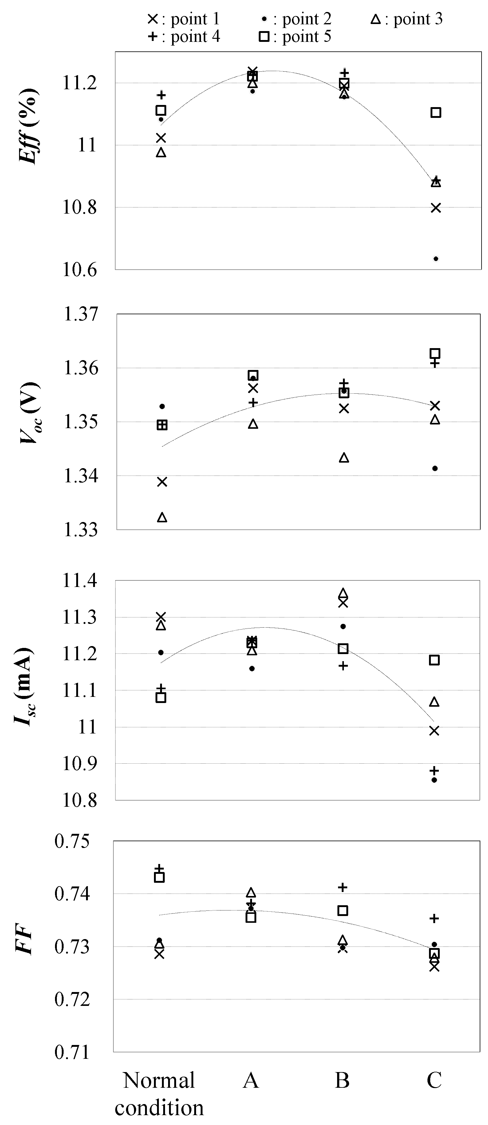
3.1. Comparison of Conversion Efficiency with the SEG Process Cell
Test results for the cells A–C are shown in
Figure 2 and
Table 3. Each of the values of
Eff,
Voc,
Isc, and
FF in
Table 3 was the average for each condition. The error bars are also the standard deviation (
δ) calculated for every condition. All results for the cells (five cells) are plotted in
Figure 2. For cell A,
Eff improved by 1.3% (0.14 points),
Voc by 0.011 V,
Isc by 0.0021, and
FF by 0.002 compared with those for the normal-condition cell. The improved
Isc and
FF were within a standard deviation range. Simply performing
SEG thus improved the
Eff,
Voc,
Isc, and
FF.
For cell B, which has the extended vacuum time, Eff improved by 1.1% (0.12 points), Voc by 0.008 V, Isc by 0.08 mA compared with those for the normal-condition cell. This result shows that SEG has similar effect to that of cell A. However, no added benefit of Eff is obtained by extending the vacuum time. However, Isc was higher than that for cells prepared under other conditions. The longer the vacuum time is, the higher the Isc available is, but the value of the changed Isc resembled the standard deviation range. The result of FF was within the margin of error.
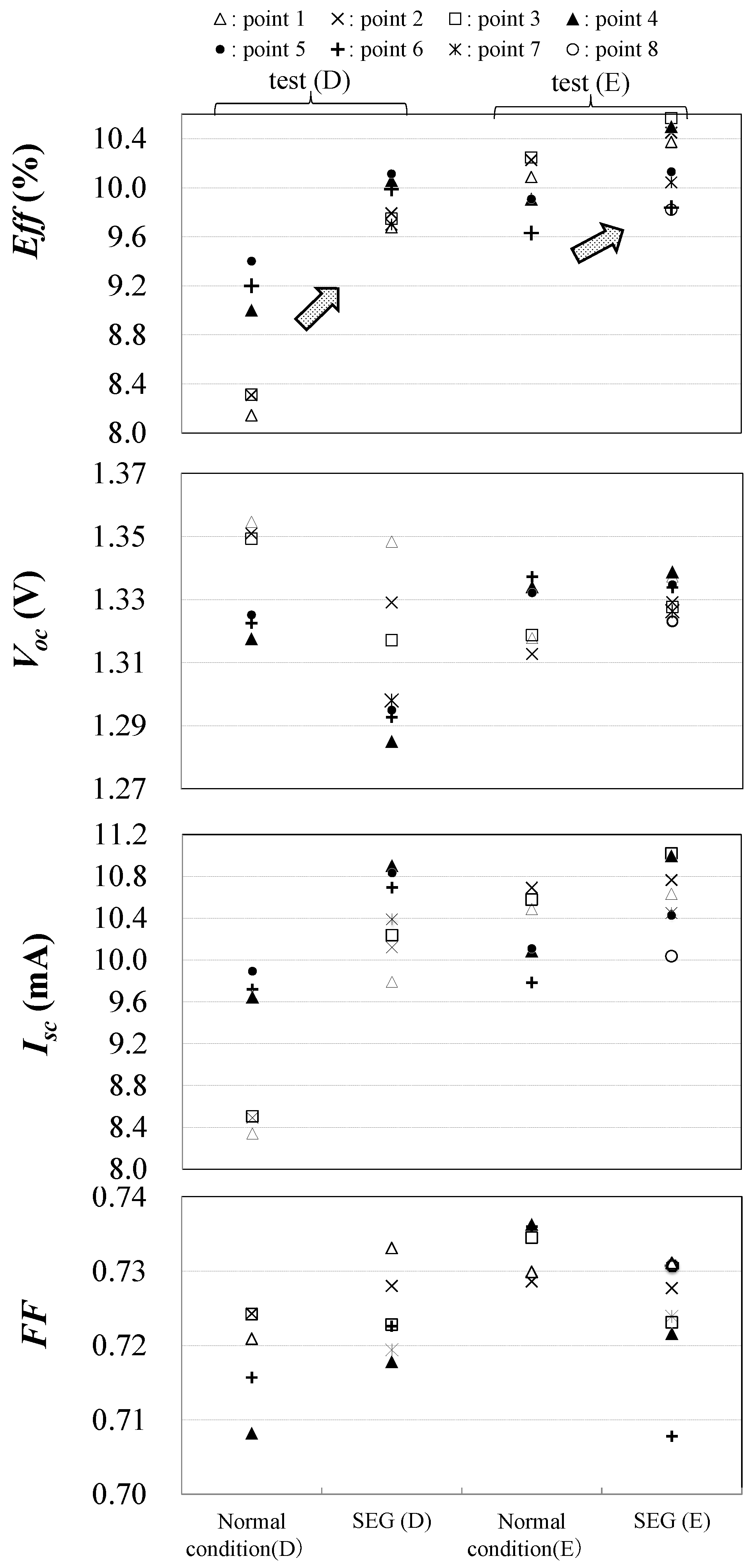
Figure 2.
Results of each test cell: normal-condition cell, cell A, cell B, and cell C. For each cell type, five cells were fabricated. Points 1-5 were cells location of substrate.
Figure 2.
Results of each test cell: normal-condition cell, cell A, cell B, and cell C. For each cell type, five cells were fabricated. Points 1-5 were cells location of substrate.
Table 3.
Results for each test cell. Each of the values of Eff, Voc, Isc, and FF was averaged for each condition. Error bars are standard deviation (δ) calculated for each condition.
Table 3.
Results for each test cell. Each of the values of Eff, Voc, Isc, and FF was averaged for each condition. Error bars are standard deviation (δ) calculated for each condition.
| | Normal-Condition Cell | Cell A | Cell B | Cell C |
|---|
| Voc (V) | 1.345 ± 0.008 | 1.355 ± 0.003 | 1.353 ± 0.005 | 1.354 ± 0.008 |
| Isc (mA) | 11.194 ± 0.089 | 11.214 ± 0.029 | 11.272 ± 0.074 | 10.996 ± 0.121 |
| FF | 0.736 ± 0.007 | 0.738 ± 0.002 | 0.734 ± 0.005 | 0.730 ± 0.003 |
| Eff (%) | 11.07 ± 0.06 | 11.21 ± 0.02 | 11.19 ± 0.03 | 10.86 ± 0.15 |
For cell C, which increased the number of SEG treatments to three, Eff decreased by 1.8% (0.21 points), Isc by 0.20 mA compared with those for the normal-condition cell. Although Voc improved by 0.008 V, it was not better than for cell A. At this time of the experiment, two SEG trials are better than three trials.
Test results for cells D and E are shown in
Table 4 and
Figure 3. For cell D,
Eff increased by 13.1% (1.14 points),
Isc by 1.33 mA,
FF by 0.005 compared with the normal-condition cell D. However,
Voc decreased by 0.027 V. For cell E,
Eff increased by 2.1% (0.21 points),
Voc by 0.006,
Isc by 0.31 mA compared with the normal-condition cell E. But increases of
Voc and
Isc were within a standard deviation range. However,
FF decreased by 0.009.
Table 4.
Results for each test of cell D and cell E. Each of the values of Eff, Voc, Isc, and FF was averaged for each condition. Normal condition of D is without SEG. Normal condition of E is without SEG. Error bars are standard deviation (δ) calculated for each condition.
Table 4.
Results for each test of cell D and cell E. Each of the values of Eff, Voc, Isc, and FF was averaged for each condition. Normal condition of D is without SEG. Normal condition of E is without SEG. Error bars are standard deviation (δ) calculated for each condition.
| | Normal Condition (E) | Cell D | Normal Condition (D) | Cell E |
|---|
| Voc (V) | 1.337 ± 0.015 | 1.309 ± 0.021 | 1.325 ± 0.009 | 1.331 ± 0.005 |
| Isc (mA) | 9.099 ± 0.660 | 10.424 ± 0.380 | 10.289 ± 0.320 | 10.597 ± 0.306 |
| FF | 0.718 ± 0.01 | 0.724 ± 0.00 | 0.7335 ± 0.00 | 0.724 ± 0.007 |
| Eff (%) | 8.72 ± 0.49 | 9.87 ± 0.167 | 10.00 ± 0.213 | 10.21 ± 0.278 |
Figure 3.
Results of each test cell: cell D, cell E, normal-condition cell D, and normal-condition cell E. For each cell type, eight cells were fabricated. Points 1-8 were cells location of substrate.
Figure 3.
Results of each test cell: cell D, cell E, normal-condition cell D, and normal-condition cell E. For each cell type, eight cells were fabricated. Points 1-8 were cells location of substrate.
The results for the all I–V characteristics are relative to the bottom cell condition, because the thickness of the i-layer (a-Si:H) of the top layer is sufficient. For cell B, for which the thickness of the i-layer on top is 240 nm, the Jsc values of the top layer and bottom layer were 11.59 and 11.31 mA/cm2, respectively, assuming external quantum efficiency (EQE). For cell D, for which the thickness of the top i-layer is 240 nm, the Jsc values of the top layer and bottom layer were 11.12 and 9.38 mA/cm2, respectively, with external quantum efficiency. The bottom layer current has a rate-controlling effect on Jsc, because a top i-layer thickness of 240 nm was adequate.
3.2. Analysis Results of Actual Crystallinity Profile of µc-Si:H along with Depth
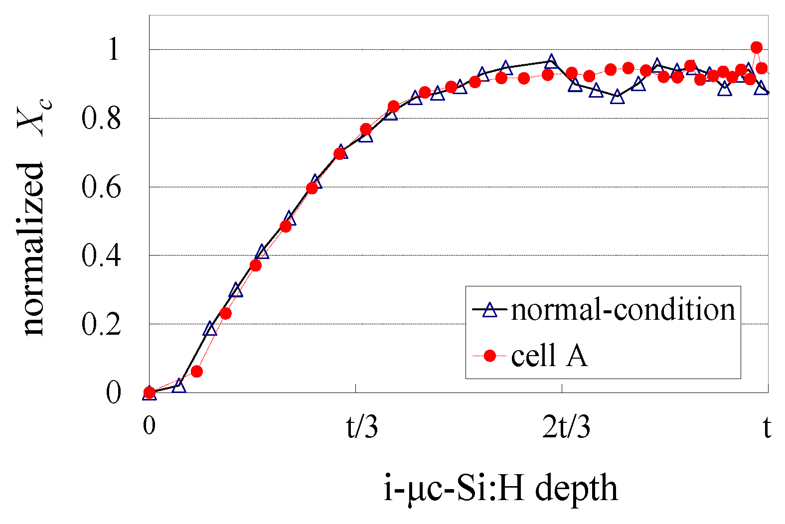
The Raman analysis results of actual crystallinity profiles of the normal-condition cell and the cell A are shown in
Figure 4. The relationship between the film thickness and
Xc is shown from the μc-Si:H thickness of zero. The obtained figure was plotted from the TCO side, and it also includes the thickness of the p-layer. This is because the p-layer of the bottom cell was μc-Si:H, but its thickness was very small (20 nm). The values of
Xc were normalized by the maximum value of
Xc among the normal-condition cell and the cell A.
Figure 4.
Results of Raman analysis of polished test cells; normal-condition cell and cell A. Values of Xc were normalized by the maximum value of Xc among normal-condition cell and cell A. Xc was expressed from the TCO side.
Figure 4.
Results of Raman analysis of polished test cells; normal-condition cell and cell A. Values of Xc were normalized by the maximum value of Xc among normal-condition cell and cell A. Xc was expressed from the TCO side.
Both the
Xc values did not show any difference between the normal-condition cell and the cell A up to the half thickness (t/2) of μc-Si:H. However,
Xc of the normal-condition cell decreased at an around 2t/3. This decrease in
Xc was probably caused by a defective region produced after the film thickness increased [
8]. These decreases in the values of
Xc were measured at four points successively. The values of
Xc are connected smoothly, unlike the surrounding values. These decreases in
Xc are therefore not due to measurement error. The decreasing
Xc during the formation of a thick film inhibited the high
Xc of µc-Si:H and effected the
Eff.
Conversely, there was no reduction in Xc in the thickness direction with cell A. It means that SEG has prevented the defective region. In addition, Xc increased with the increasing film thickness, and a maximum Xc was confirmed. In the comparison of the Xc profiles between the normal-condition cell and cell A, SEG yielded high values of Xc.
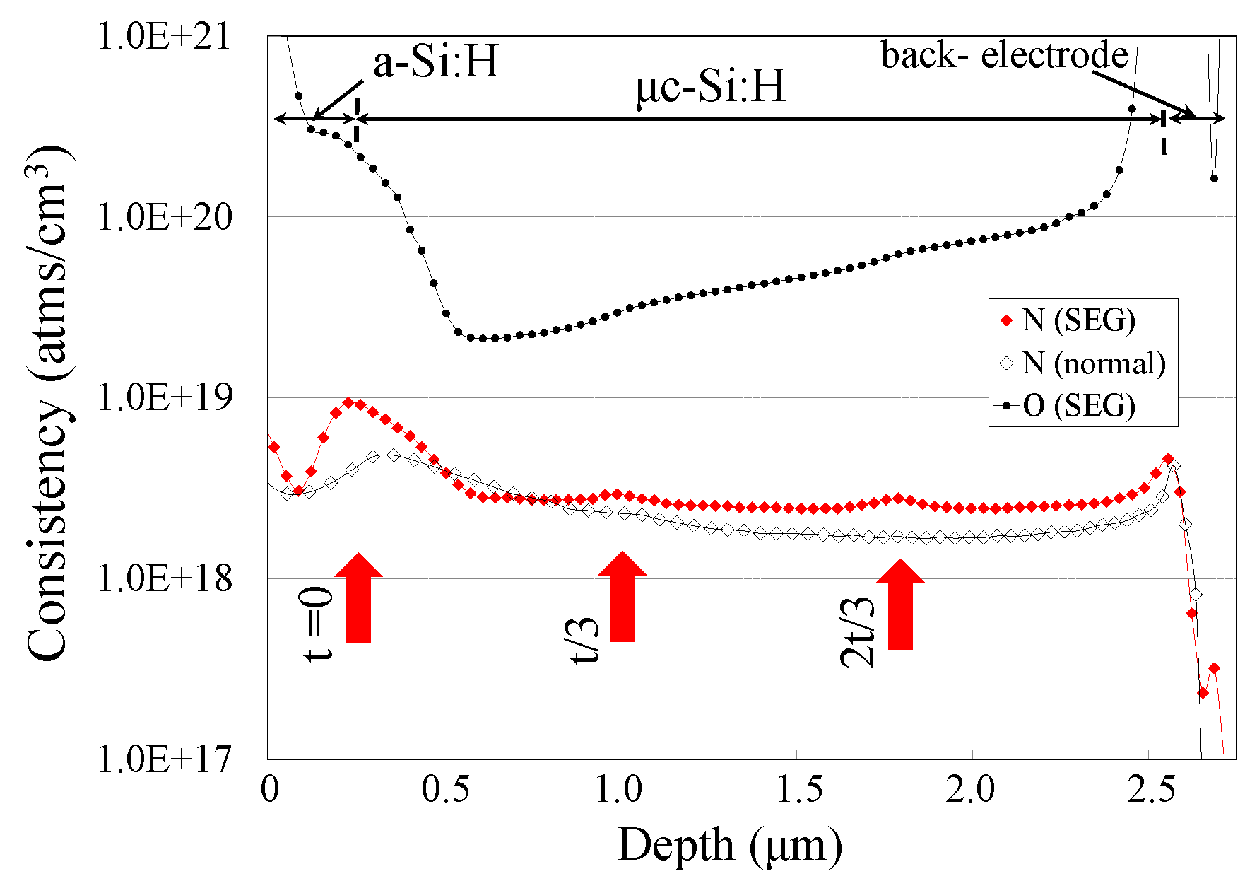
3.3. Secondary Ion Mass Spectrometry Analyses with Cell
Nitrogen impurity levels were analyzed with the normal-condition cell and the cell A shown in
Figure 5. Since it was analyzed from the back-contact side by SIMS, the results were expressed in the direction reverse to the deposition direction. In the no
SEG region of μc-Si:H, nitrogen was detected by about 2.5 × 10
18 (atom/cm
3). Nitrogen increased by approximately 10%–15% (about 2.9 × 10
18 (atom/cm
3)) in the layers of the
SEG region: at t/3 and 2t/3. In comparison, under normal conditions, it did not change significantly during the i-layer deposition. Nitrogen gas was never been used at all even after the deposition process in the process chamber. This nitrogen was brought form outside air by the substrate of the cell or film, or was released as degassing from the wall of the deposition chamber. Nitrogen gas was incorporated into the μc-Si:H [
24].
Figure 5.
Profile of impurities about nitrogen and oxygen in cell A which used the SEG by SIMS. The nitrogen profile for normal-condition cells is also shown. Results were expressed in the direction reverse to the deposition direction.
Figure 5.
Profile of impurities about nitrogen and oxygen in cell A which used the SEG by SIMS. The nitrogen profile for normal-condition cells is also shown. Results were expressed in the direction reverse to the deposition direction.
On the one hand, between the a-Si:H layer and the μc-Si:H layer, nitrogen was detected with a threefold increase (1.0 × 10¹⁹ atom/cm3) compared to other layers of μc-Si:H. When the processing equipment was changed from a-Si:H process to μc-Si:H process, cells were at once exposed to the atmosphere.
Oxygen impurity levels were analyzed with the cell A shown in
Figure 5. Slightly more was detected in the
SEG region of μc-Si:H in the same way as nitrogen. This was caused by the
SEG. However, a difference level comparison between the
SEG layer and no
SEG layer was not as high as for nitrogen. The details are not noted here because the differences were negligible.
3.4. Film Analysis with FTIR and Raman
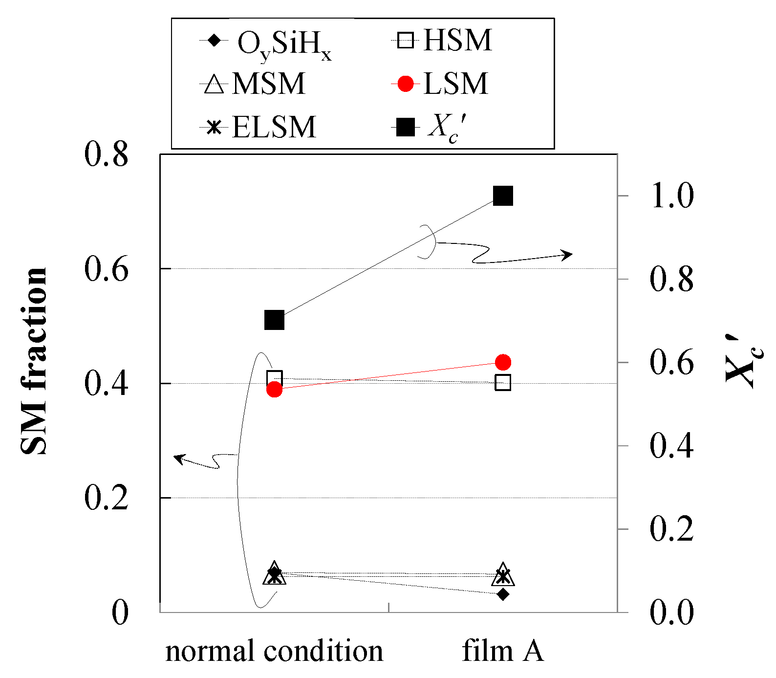
As a comparison of the normal-condition film and film A, the results of analysis by Raman spectrometry and FTIR are shown in
Figure 6. The value of
Xc′ was normalized by a maximum value of film A.
Figure 6.
Analyzed results of film tests, normal-condition film and film A, by Raman spectrometry and FTIR. The values of Xc′ were normalized by the value of the film A.
Figure 6.
Analyzed results of film tests, normal-condition film and film A, by Raman spectrometry and FTIR. The values of Xc′ were normalized by the value of the film A.
The film quality was different from the quality of the cell because that was deposited on the flat-glass rather than textured-TCO. The difference was spread significantly by the flat substrate. Thus, this confirmation was a relative comparison.
In film A, the LSM value was detected as stronger compared to a normal-condition film. This means that the film A contains a large amount of silicon monohydride (Si–H), so this component is expected to terminate the dangling bonds in µc-Si:H [
25]. Also, O
ySiH
x which means crystalline grain boundaries was fewer than in the normal-condition film [
19]. Owing to the
SEG, the quality of μc-Si:H became better on the evaluation of the film.
However, Xc′ of film A was higher than that of the normal condition film. The higher Xc′, higher LSM, and lower OySiHx of i-μc-Si:H such as film A can yield a high solar cell Eff. Thus, SEG successfully improved the µc-Si:H quality.
4. Discussion
To reduce the defective region correlation with the film thickness gain, the
SEG process was carried out. Under its influence, as seen in
Figure 4,
Xc of μc-Si:H does not decrease the value of
Xc during the process of forming a thick film. As a result, the cell achieved a high
Xc and the value of
Xc′ increased. Also, as seen in
Figure 6, the LSM value was detected as stronger than in a normal-condition film. Increasing the amorphous component such as LSM improved the quality of μc-Si:H by terminating the dangling bonds in µc-Si:H [
26,
27]. Eventually, the
Eff,
Voc, and
FF of cell A improved.
On the other hand, the difference between cell A and cell B, which was the test of discharge stop time, increased the
Isc. This characteristic difference was led not only by the initial discharge instability, but also by the impurity incorporation. Nitrogen and oxygen were also detected on the
SEG cell with SIMS. On another hand, the
Xc of μc-Si:H is changed by nitrogen, according to Ehara [
28]. In our study of film A, the LSM which corresponds to the amorphous component (Si–H) was increased using the
SEG layer. From this circumstantial evidence, it is reasonable to assume that nitrogen, which comes from the
SEG process, increased the amorphous component. More nitrogen in cell B increases the N donor in the amorphous component and may increase the charged Si dangling bonds [
29] and finally increased the
Isc more than cell A. Or oxygen was increased by
SEG impurities in the growing film [
30].
After the
SEG, the amorphous component was deposited in the precursor defective region. The crystalline direction of μc-Si:H, which grows perpendicular to the textured substrate, was changed by the amorphous component [
31]. As a result, collisions with the neighboring grains were reduced. The oxide might have influenced the
Xc as well as nitrogen [
32]. On the another front, a large amount of nitrogen was detected in the earlier thickness stage of μc-Si:H (around t = 0) in
Figure 5. In exactly the same way, the value of
Xc became low at its earlier thickness stage (around t = 0) in
Figure 4. More nitrogen, which was carried from outside, might change it.
Moreover, in many of the
SEG cell Cs,
Voc increased, and
Isc and
FF decreased. Since the μc-Si:H film formation was stopped before the
Xc growth increases, the continuous deposition time of μc-Si:H was shortened, and much of the amorphous phase easily formed [
8]. Therefore, much of the amorphous phase increased
Voc [
3], and decreased
Isc [
33]. Since the shunt resistance was increased by the rising number of
SEG,
FF was decreased [
34].
The other cells (D, E) showed improved Eff, even when certain conditions were changed. These results showed repeatability in how the SEG process improves efficiency. However, variations (increase or decrease) of Voc, Isc and FF did not show the same pattern. Thus, Eff changed depending on each condition. This is because the solar characteristic of i-μc-Si:H are determined by the proportion of μc-Si:H and a-Si:H. As a result, the best number for SEG varies depending on the i-layer condition. Double SEG does not always produce a high Eff, even though it showed improvement in this experiment. The number of SEGs can be determined by how high Xc becomes.


