
Reconfiguration of Urban Photovoltaic Arrays Using Commercial Devices


Abstract
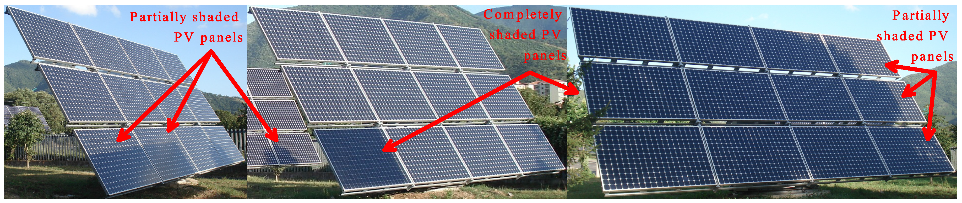
:1. Introduction
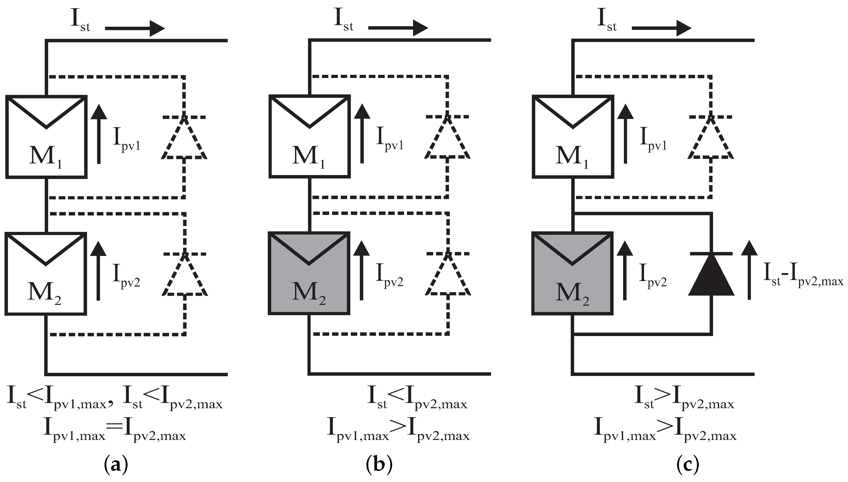
2. Reconfiguration of PV Systems


3. Reconfiguration of Panels Based on Experimental Data
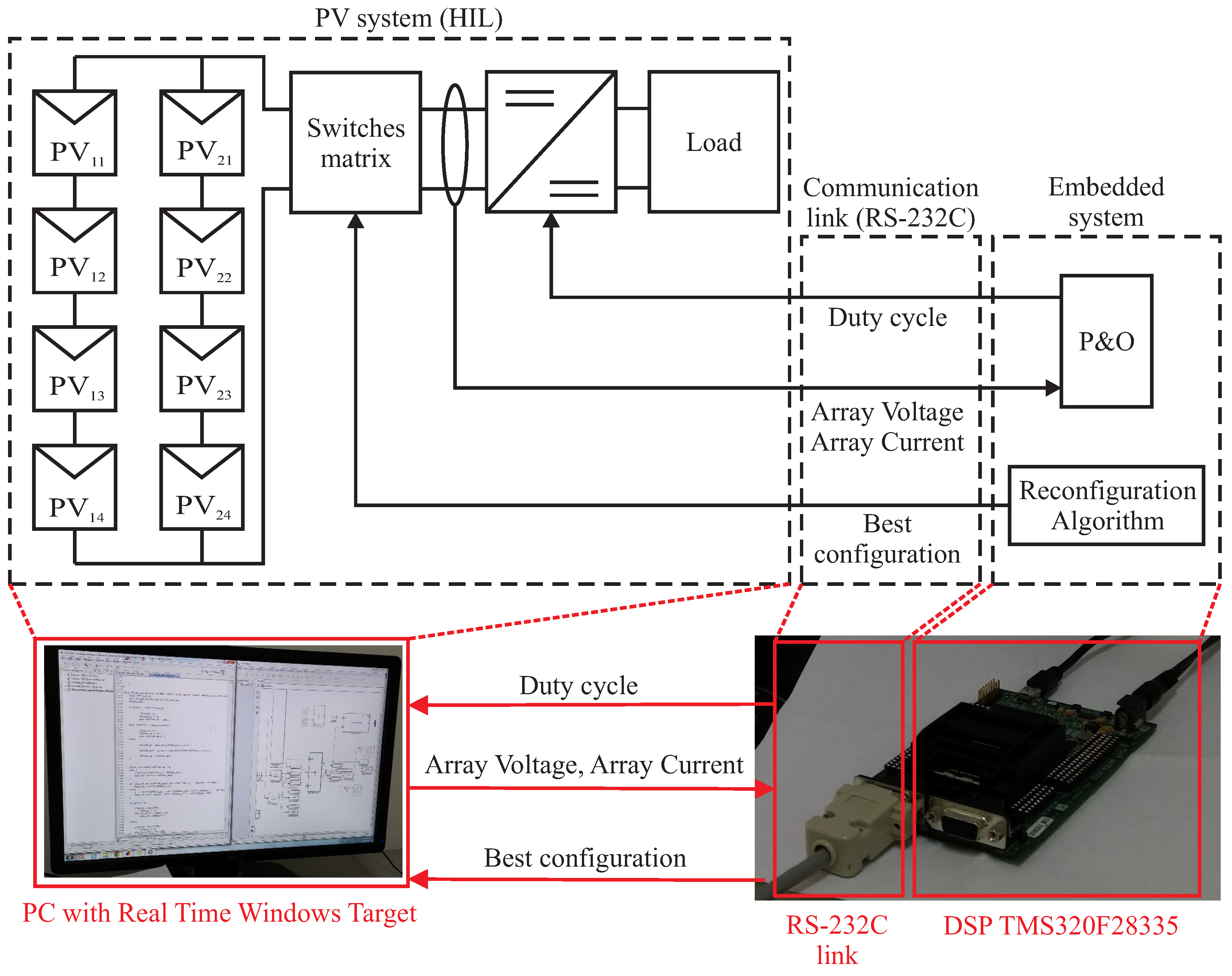
3.1. Structure of the Reconfiguration System
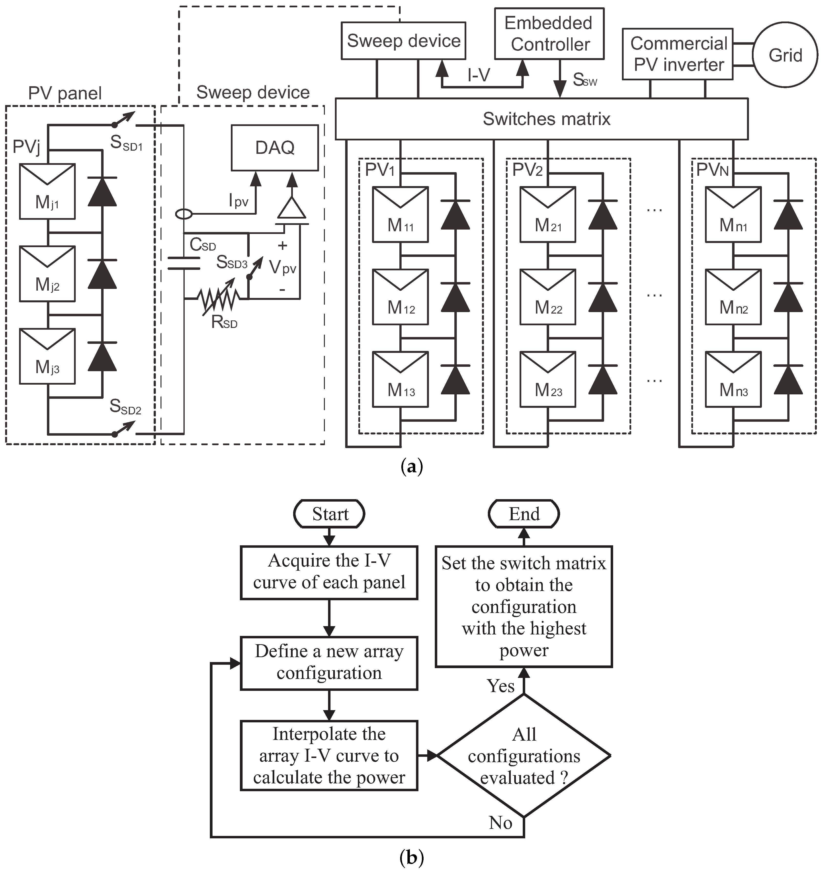
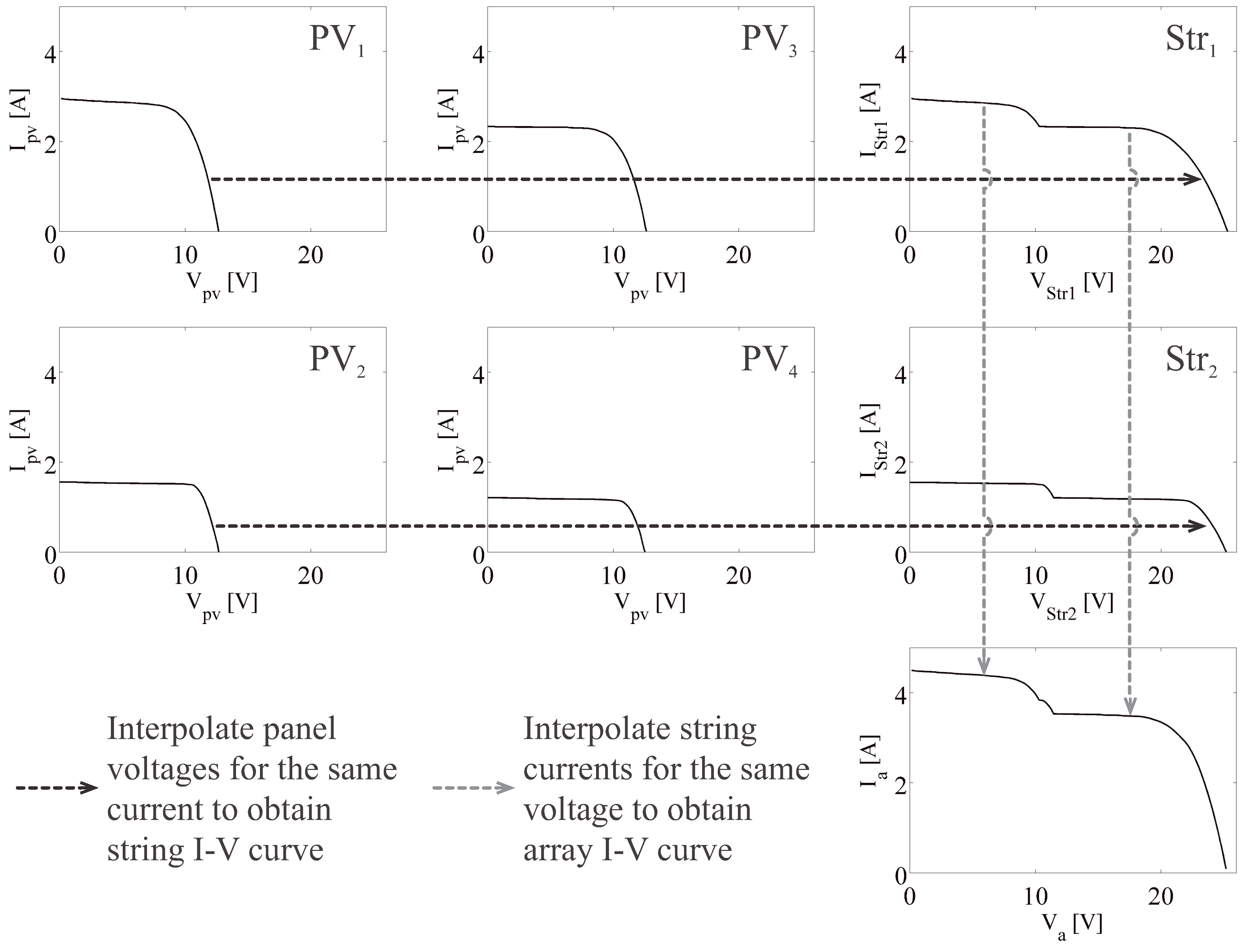
3.2. Evaluation of Possible Array Configurations
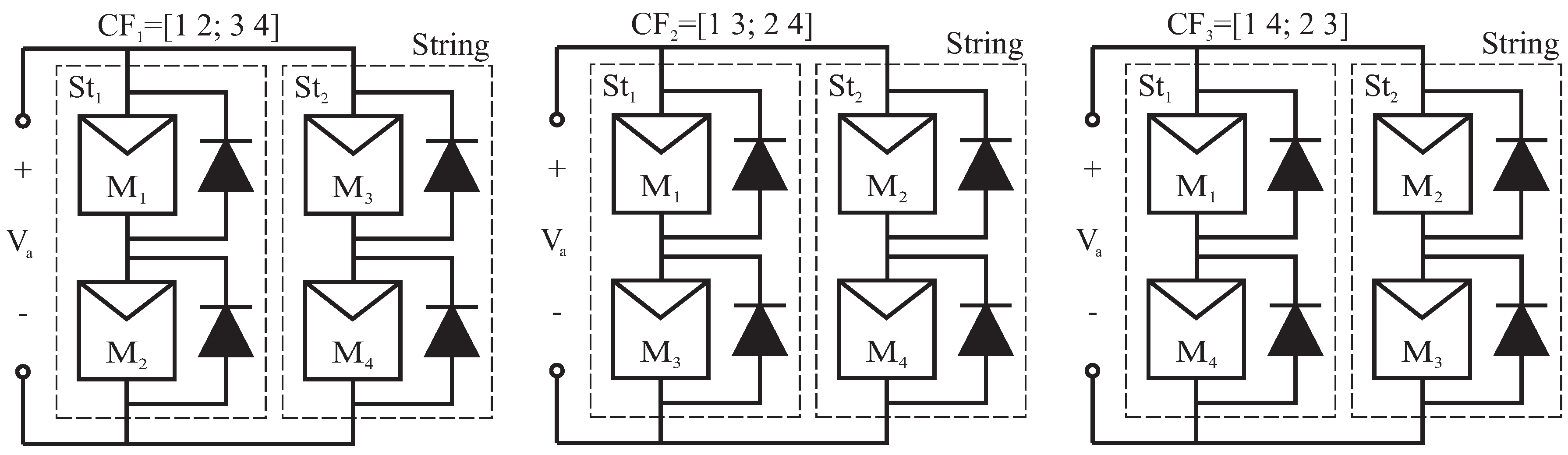
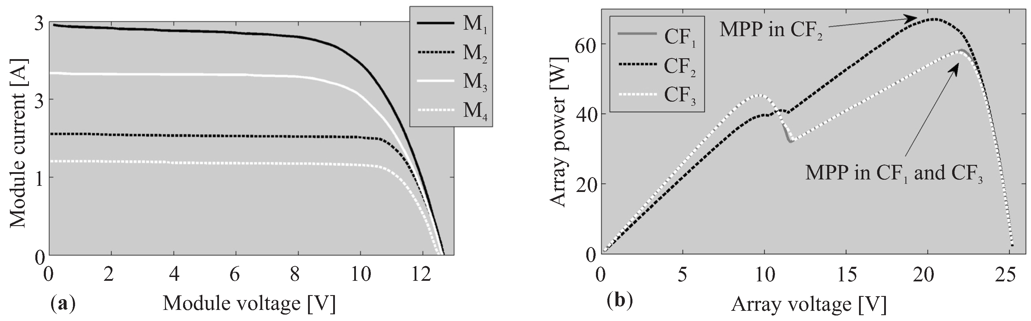
3.3. Application Example Based on Commercial Devices

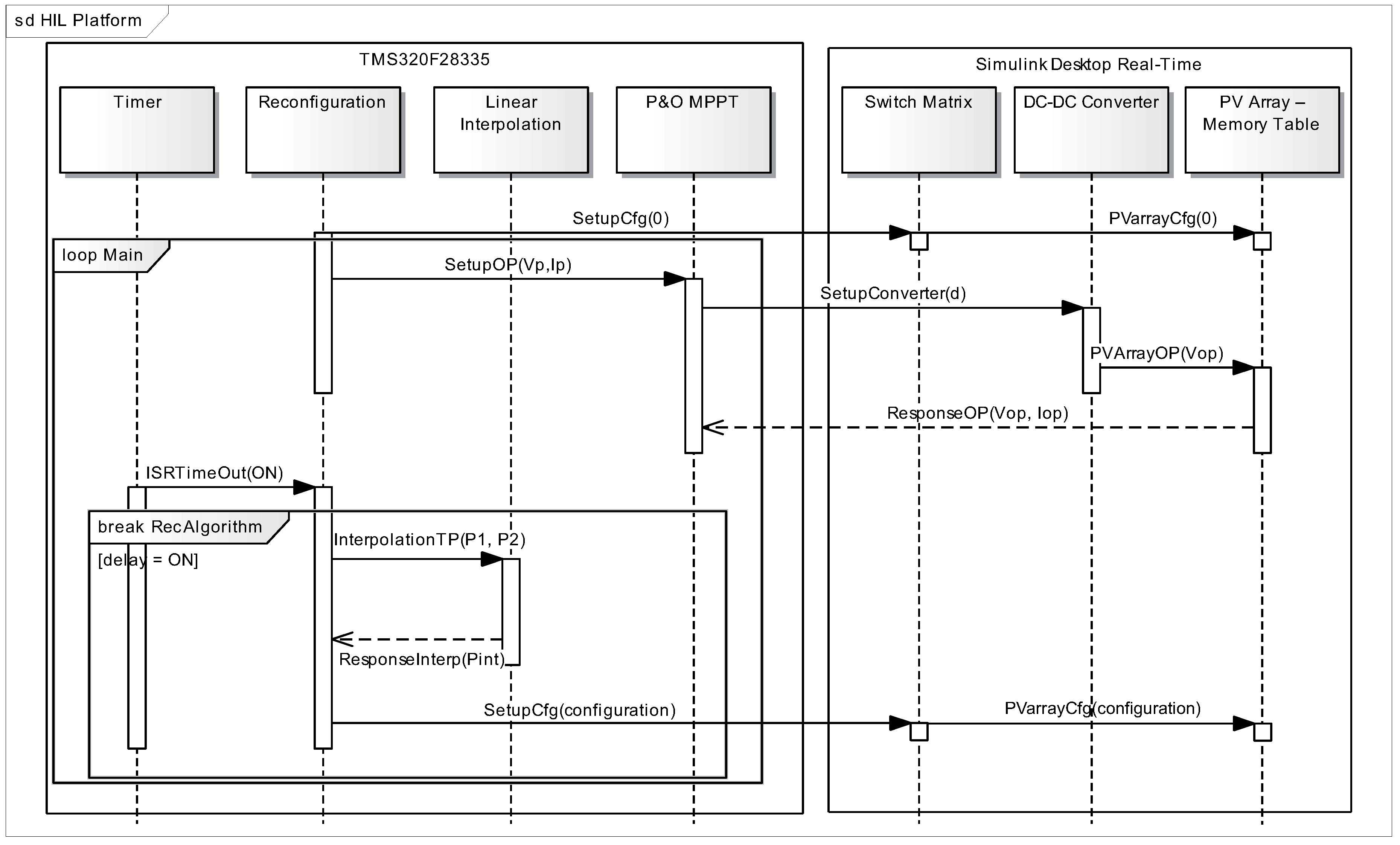
4. Simulation Platform Implementation Using Commercial Devices


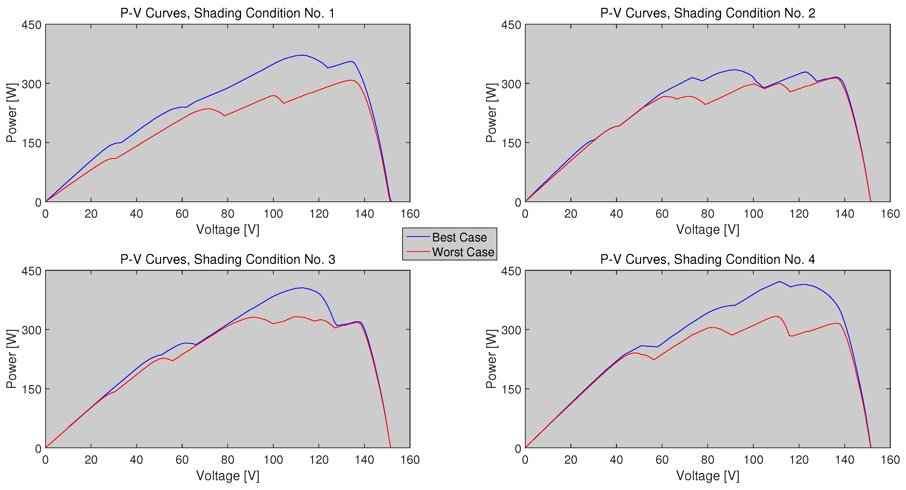
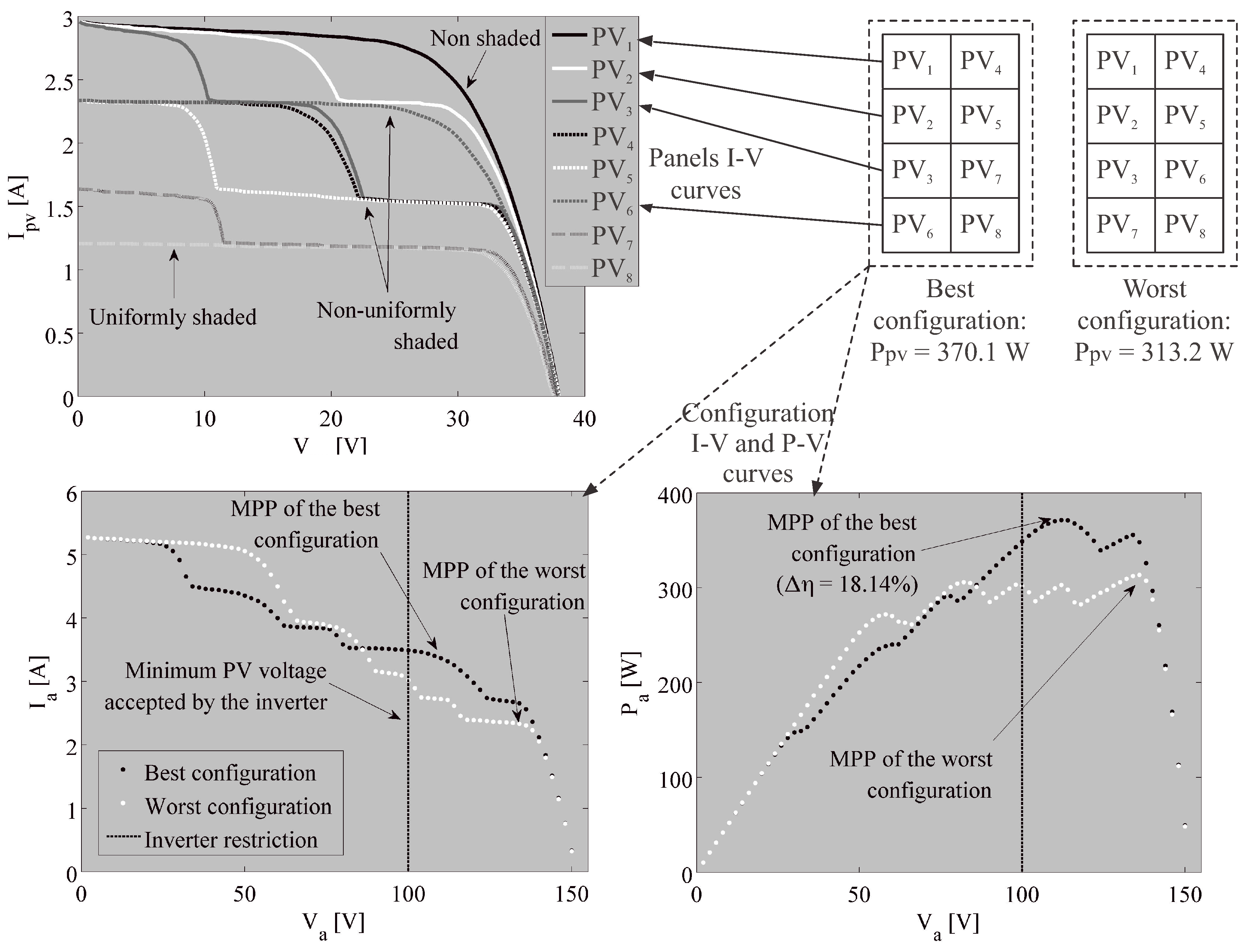
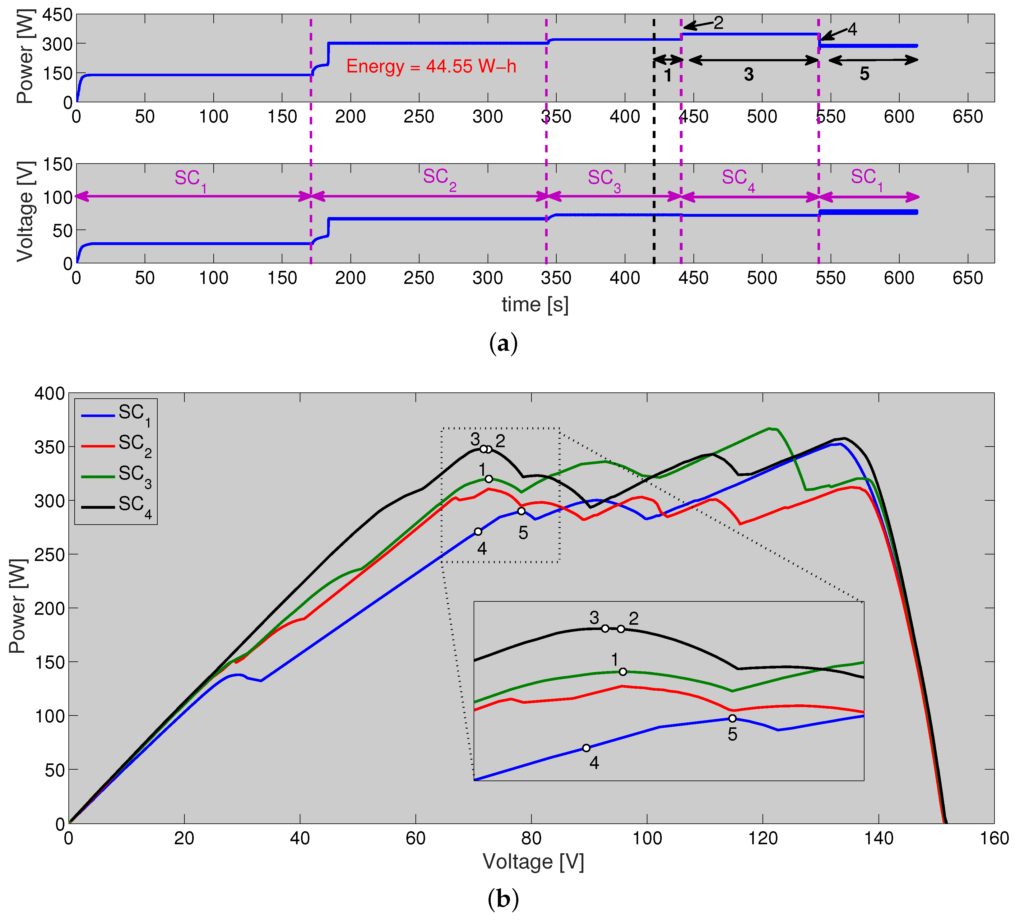
5. Simulation Results Based on Experimental Data
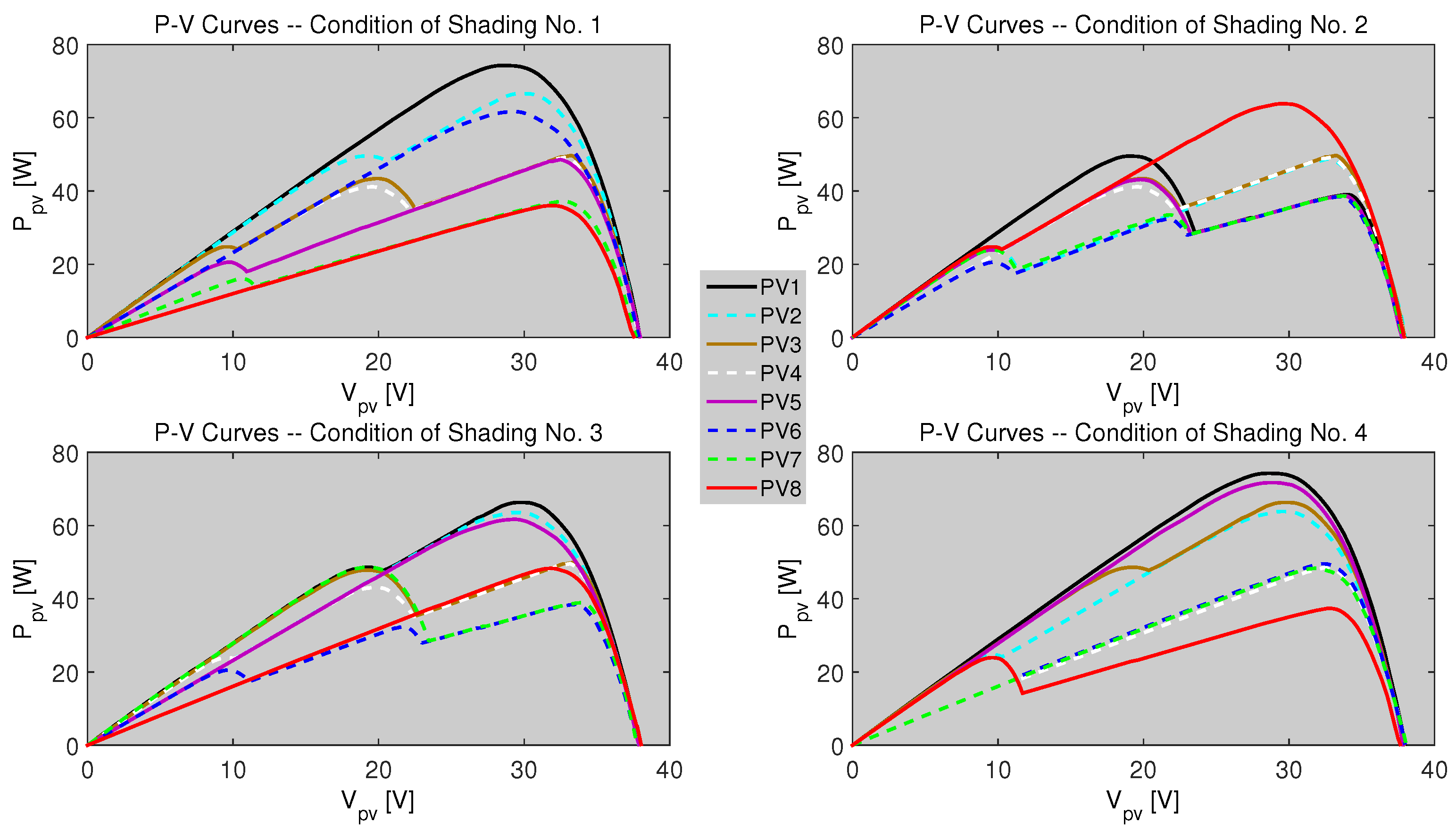
5.1. Simulated Shading Conditions
- Condition No. 1 (SC (SC, shading condition): PV, PV and PV are uniformly shaded; hence, they have a single MPP. PV, PV, PV and PV have one shaded module (i.e., two MPPs), while PV has two partially-shaded modules (i.e., three MPPs).
- Condition No. 2 (SC): PV and PV have, each, two shaded modules, while the others panels have one shaded module.
- Condition No. 3 (SC): PV and PV are uniformly shaded; moreover, PV, PV, PV and PV have one shaded module, while PV and PV have two shaded modules.
- Condition No. 4 (SC): PV, PV and PV are uniformly shaded. PV, PV, PV, PV and PV have one shaded module.


| Shading condition | Best configuration | Worst configuration | Power increment | |||
|---|---|---|---|---|---|---|
| Number | Power (W) | Number | Power (W) | (W) | (%) | |
| 1 | 8 | 371.426 | 13 | 304.982 | 66.444 | 21.8 |
| 2 | 14 | 334.356 | 31 | 313.522 | 20.834 | 6.6 |
| 3 | 22 | 405.929 | 28 | 332.975 | 72.953 | 21.9 |
| 4 | 4 | 421.665 | 13 | 333.620 | 88.045 | 26.4 |
| Configuration | Order of PV panels | Description | |
|---|---|---|---|
| CF | Initial with RA | ||
| CF | Best for SC | ||
| CF | Best for SC | ||
| CF | Worst for SC and SC | ||
| CF | Best for SC | ||
| CF | Without RA | ||
| CF | Best for SC | ||
| CF | Worst for SC | ||
| CF | Worst for SC |
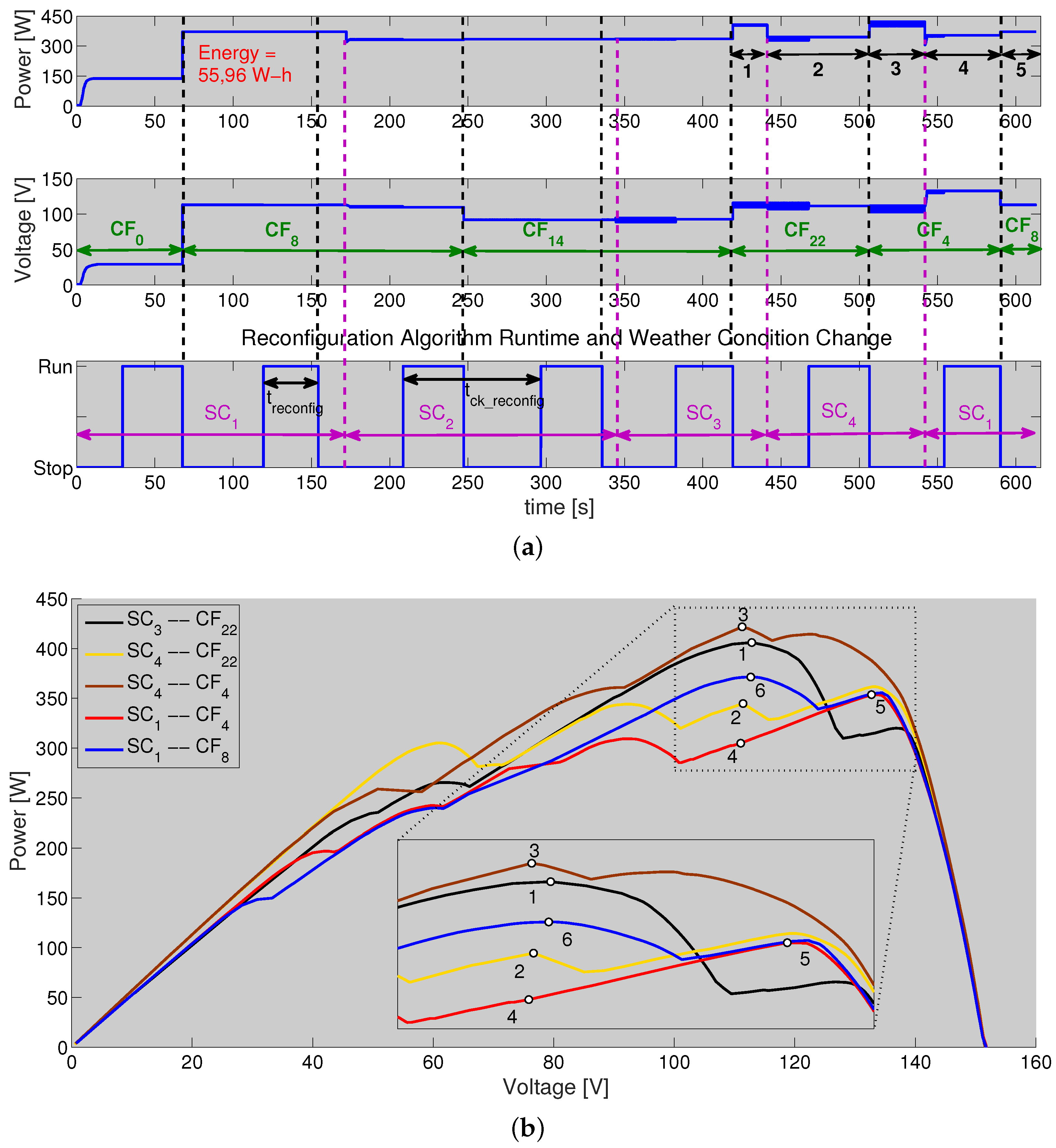
5.2. Sampling Time and Time Delay of the Sweep Device and Switches
5.3. Dynamic Simulation of the Reconfiguration System

5.4. Calculation Burden of the Reconfiguration Algorithm
| Shading condition | i | (s) | Deviation from average | |
|---|---|---|---|---|
| SC | 1 | 33.409 | 5,008,845,577 | −7.5% |
| SC | 2 | 37.180 | 5,574,212,894 | 2.9% |
| SC | 3 | 36.183 | 5,424,737,631 | 0.2% |
| SC | 4 | 38.388 | 5,755,322,339 | 6.3% |
| SC | 5 | 37.591 | 5,635,832,084 | 4.0% |
| SC | 6 | 36.589 | 5,485,607,196 | 1.3% |
| SC | 7 | 33.558 | 5,031,184,408 | −7.1% |
5.5. Tests without Accounting for Array Reconfiguration
6. Conclusions
Acknowledgments
Author Contributions
Conflicts of Interest
References
- La Manna, D.; li Vigni, V.; Riva Sanseverino, E.; di Dio, V.; Romano, P. Reconfigurable electrical interconnection strategies for photovoltaic arrays: A review. Renew. Sustain. Energy Rev. 2014, 33, 412–426. [Google Scholar] [CrossRef]
- Parlak, K.S. PV array reconfiguration method under partial shading conditions. Int. J. Electr. Power Energy Syst. 2014, 63, 713–721. [Google Scholar] [CrossRef]
- Fathabadi, H. Lambert W function-based technique for tracking the maximum power point of PV modules connected in various configurations. Renew. Energy 2015, 74, 214–226. [Google Scholar] [CrossRef]
- Ramaprabha, R.; Mathur, B.L. A comprehensive review and analysis of solar photovoltaic array configurations under partial shaded conditions. Int. J. Photoenergy 2012, 2012, 16. [Google Scholar] [CrossRef]
- SMA Solar Technology AG. Sunny Boy 1200/1700/2500/3000. In Datasheet SB1200_3000-DEN110712; SMA Solar Technology AG: Niestetal, Germany, 2004; Available online: http://www.el-tec.nl/include/nl/downloads/SB12003000-DEN110712W.pdf (accessed on 1 October 2015).
- SolarEdge Technologies Inc. SolarEdge Single Phase Inverters SE2200-SE6000; SolarEdge Technologies Inc.: Fremont, CA, USA, 2014. [Google Scholar]
- Balato, M.; Vitelli, M. A new control strategy for the optimization of distributed MPPT in PV applications. Int. J. Electr. Power Energy Syst. 2014, 62, 763–773. [Google Scholar] [CrossRef]
- Balato, M.; Vitelli, M. Optimization of distributed maximum power point tracking PV applications: The scan of the power vs. voltage input characteristic of the inverter. Int. J. Electr. Power Energy Syst. 2014, 60, 334–346. [Google Scholar] [CrossRef]
- Subudhi, B.; Pradhan, R. A comparative study on maximum power point tracking techniques for photovoltaic power systems. IEEE Trans. Sustain. Energy 2013, 4, 89–98. [Google Scholar] [CrossRef]
- Gules, R.; de Pellegrin Pacheco, J.; Hey, H.; Imhoff, J. A maximum power point tracking system with parallel connection for PV stand-alone applications. IEEE Trans. Ind. Electr. 2008, 55, 2674–2683. [Google Scholar] [CrossRef]
- Esram, T.; Chapman, P. Comparison of photovoltaic array maximum power point tracking techniques. IEEE Trans. Energy Convers. 2007, 22, 439–449. [Google Scholar] [CrossRef]
- Qi, J.; Zhang, Y.; Chen, Y. Modeling and maximum power point tracking (MPPT) method for PV array under partial shade conditions. Renew. Energy 2014, 66, 337–345. [Google Scholar] [CrossRef]
- Bastidas-Rodriguez, J.; Franco, E.; Petrone, G.; Andrés Ramos-Paja, C.; Spagnuolo, G. Maximum power point tracking architectures for photovoltaic systems in mismatching conditions: A review. IET Power Electr. 2014, 7, 1396–1413. [Google Scholar] [CrossRef]
- Vincenzo, M.C.D.; Infield, D. Detailed PV array model for non-uniform irradiance and its validation against experimental data. Sol. Energy 2013, 97, 314–331. [Google Scholar] [CrossRef]
- Bastidas-Rodriguez, J.D.; Ramos-Paja, C.A.; Saavedra-Montes, A.J. Reconfiguration analysis of photovoltaic arrays based on parameters estimation. Simul. Model. Pract. Theory 2013, 35, 50–68. [Google Scholar] [CrossRef]
- El-Dein, M.; Kazerani, M.; Salama, M. Optimal photovoltaic array reconfiguration to reduce partial shading losses. IEEE Trans. Sustain. Energy 2013, 4, 145–153. [Google Scholar] [CrossRef]
- Trina Solar. PDG5: The Dual Glass Module. In Datasheet TSM_EN_August_2014_A(US); Trina Solar Limited: 100 Century Center: San Jose, CA, USA, 2014; Available online: http://www.trinasolar.com/HtmlData/downloads/us/USDatasheetPDG5.pdf (accessed on 30 September 2015).
- KYOCERA Solar, Inc. KD F Series Family. In Datasheet KD Modules 032114; KYOCERA Solar, Inc.: Scottsdale, AZ, USA, 2013; Available online: http://www.kyocerasolar.com/assets/001/5133.pdf (accessed on 30 september 2015).
- Ji, Y.H.; Jung, D.Y.; Kim, J.G.; Kim, J.H.; Lee, T.W.; Won, C.Y. A real maximum power point tracking method for mismatching compensation in PV array under partially shaded conditions. IEEE Trans. Power Electr. 2011, 26, 1001–1009. [Google Scholar] [CrossRef]
- Picault, D.; Raison, B.; Bacha, S.; de la Casa, J.; Aguilera, J. Forecasting photovoltaic array power production subject to mismatch losses. Sol. Energy 2010, 84, 1301–1309. [Google Scholar] [CrossRef]
- Velasco-Quesada, G.; Guinjoan-Gispert, F.; Pique-Lopez, R.; Roman-Lumbreras, M.; Conesa-Roca, A. Electrical PV array reconfiguration strategy for energy extraction improvement in grid-connected PV systems. IEEE Trans. Ind. Electr. 2009, 56, 4319–4331. [Google Scholar] [CrossRef]
- Karatepe, E.; Boztepe, M.; çolak, M. Development of a suitable model for characterizing photovoltaic arrays with shaded solar cells. Sol. Energy 2007, 81, 977–992. [Google Scholar] [CrossRef]
- Bishop, J.W. Computer simulation of the effects of electrical mismatches in photovoltaic cell interconnection circuits. Sol. Cells 1988, 25, 73–89. [Google Scholar] [CrossRef]
- Petrone, G.; Ramos-Paja, C. Modeling of photovoltaic fields in mismatched conditions for energy yield evaluations. Electr. Power Syst. Res. 2011, 81, 1003–1013. [Google Scholar] [CrossRef]
- Bastidas, J.D.; Franco, E.; Petrone, G.; Ramos-Paja, C.A.; Spagnuolo, G. A model of photovoltaic fields in mismatching conditions featuring an improved calculation speed. Electr. Power Syst. Res. 2013, 96, 81–90. [Google Scholar] [CrossRef]
- National Instruments. NI 2810/2811/2812/2813/2814 Specifications. In Datasheet 375527E; National Instruments Corporation: Austin, TX, USA, 2012. [Google Scholar]
- Pickering Interfaces Ltd. 40-550 Power Matrix Module. Issue 7.1. May 2014. Available online: http://www.pickeringtest.com/content/private/datasheets/40-550D.pdf (accessed on 9 October 2015).
- BP Solar. BP 2150S. In Datasheet 01-3001-2A; BP group: 501 Westlake Park Boulevard Houston: Houston TX, USA, 2002; Available online: http://www.solarcellsales.com/techinfo/docs/BP2150S-DataSheet.pdf (accessed on 19 August 2015).
- SolarEdge Technologies Inc. SolarEdge Power Optimizer Module Add-On P300/P350/P404/P405/P500; 47505 Seabridge Drive, Fremont, CA, USA, 2015. [Google Scholar]
- Ramos-Paja, C.A.; Bastidas-Rodriguez, J.D.; Saavedra-Montes, A.J. Experimental validation of a model for photovoltaic arrays in total cross-tied configuration. DYNA 2013, 80, 191–199. [Google Scholar]
- Ramabadran, R.; Gandhi Salai, R.; Mathur, B. Effect of shading on series and parallel connected solar PV modules. Mod. Appl. Sci. 2009, 3, 32–41. [Google Scholar] [CrossRef]
- Aranda, E.; Galan, J.; de Cardona, M.; Marquez, J. Measuring the I-V curve of PV generators. IEEE Ind. Electr. Mag. 2009, 3, 4–14. [Google Scholar] [CrossRef]
- Bitron. Optimization, monitoring and safety for photovoltaics. In Datasheet endana, Intelligence applied to photovoltaics; Bitron SPA: Grugliasco, TO, Italy; Available online: http://www.smartblue.de/wp-content/uploads/2012/06/ENDANA-Brochure-EN.pdf (accessed on 12 October 2015).
- Alahmad, M.; Chaaban, M.A.; Lau, S.K.; Shi, J.; Neal, J. An adaptive utility interactive photovoltaic system based on a flexible switch matrix to optimize performance in real-time. Sol. Energy 2012, 86, 951–963. [Google Scholar] [CrossRef]
- Nguyen, D.; Lehman, B. An adaptive solar photovoltaic array using model-based reconfiguration algorithm. IEEE Trans. Ind. Electr. 2008, 55, 2644–2654. [Google Scholar] [CrossRef]
- Romero-Cadaval, E.; Spagnuolo, G.; Garcia Franquelo, L.; Ramos-Paja, C.; Suntio, T.; Xiao, W. Grid-connected photovoltaic generation plants: Components and operation. IEEE Ind. Electr. Mag. 2013, 7, 6–20. [Google Scholar] [CrossRef] [Green Version]
- Lo Brano, V.; Orioli, A.; Ciulla, G. On the experimental validation of an improved five-parameter model for silicon photovoltaic modules. Sol. Energy Mater. Sol. Cells 2012, 105, 27–39. [Google Scholar] [CrossRef]
- Salmi, T.; Bouzguenda, M.; Gastli, A.; Masmoudi, A. MATLAB/simulink based modeling of photovoltaic cell. Int. J. Renew. Energy Res. 2012, 2, 213–218. [Google Scholar]
- Villalva, M.G.; Gazoli, J.R.; Filho, E. Comprehensive approach to modeling and simulation of photovoltaic arrays. IEEE Trans. Power Electr. 2009, 24, 1198–1208. [Google Scholar] [CrossRef]
- Wang, Y.J.; Hsu, P.C. Analysis of partially shaded PV modules using piecewise linear parallel branches model. World Acad. Sci. Eng. Technol. 2009, 3, 2360–2366. [Google Scholar]
- Obane, H.; Okajima, K.; Oozeki, T.; Ishii, T. PV system with reconnection to improve output under nonuniform illumination. IEEE J. Photovolt. 2012, 2, 341–347. [Google Scholar] [CrossRef] [Green Version]
- Villa, L.F.L.; Picault, D.; Raison, B.; Bacha, S.; Labonne, A. Maximizing the power output of partially shaded photovoltaic plants through optimization of the interconnections among its modules. IEEE J. Photovolt. 2012, 2, 154–163. [Google Scholar] [CrossRef]
- Texas Instruments Incorporated. Code Composer Studio (CCS) Integrated Development Environment (IDE)-CCSTUDIO-TI Tool Folder. Avaiable online: http://www.ti.com/tool/ccstudio (accessed on 31 July 2015).
- BP Solat Pty Ltd. BP 3165. In Datasheet 4039A-2; Houston, TX, USA, 2007; Avaiable online: https://www.solarpanelsaustralia.com.au/downloads/bpsolarbp3165.pdf (accessed on 5 August 2015).
- Chris Washington. Real-Time Testing: Hardware-in-the-Loop and Beyond; National Instruments Corporation: Austin, TX, USA, 2010. [Google Scholar]
- MathWorks, Inc. Simulink Desktop Real-Time. 2015. Avaiable online: http://cn.mathworks.com/products/simulink-desktop-real-time/ (accessed on 19 October 2015).
- Malla, S. Perturb and Observe (P & O) Algorithm for PV MPPT. 26 December 2012. Avaiable online: http://www.mathworks.com/matlabcentral/fileexchange/39641-perturb-and-observe–p-o–algorithm-for-pv-mppt (accessed on 24 June 2015).
- Texas Instruments. TMS320F28335, TMS320F28334, TMS320F28332, TMS320F28235, TMS320F28234, TMS320F28232 Digital Signal Controllers (DSCs). In Data Manual SPRS439M; Texas Instruments Incorporated: Dallas, TX, USA, 2007. [Google Scholar]
- Hoff, T.E.; Perez, R. Quantifying PV power output variability. Sol. Energy 2010, 84, 1782–1793. [Google Scholar] [CrossRef]
© 2015 by the authors; licensee MDPI, Basel, Switzerland. This article is an open access article distributed under the terms and conditions of the Creative Commons by Attribution (CC-BY) license (http://creativecommons.org/licenses/by/4.0/).
Share and Cite
Serna-Garcés, S.I.; Bastidas-Rodríguez, J.D.; Ramos-Paja, C.A. Reconfiguration of Urban Photovoltaic Arrays Using Commercial Devices. Energies 2016, 9, 2. https://doi.org/10.3390/en9010002
Serna-Garcés SI, Bastidas-Rodríguez JD, Ramos-Paja CA. Reconfiguration of Urban Photovoltaic Arrays Using Commercial Devices. Energies. 2016; 9(1):2. https://doi.org/10.3390/en9010002
Chicago/Turabian StyleSerna-Garcés, Sergio Ignacio, Juan David Bastidas-Rodríguez, and Carlos Andrés Ramos-Paja. 2016. "Reconfiguration of Urban Photovoltaic Arrays Using Commercial Devices" Energies 9, no. 1: 2. https://doi.org/10.3390/en9010002