Article

Current Mode Control for LLC Series Resonant DC-to-DC Converters †

1
Power Electronics Team, LG Electronics, Pyungtaek-city, Kyungki-do 451-713, Korea
2
School of Electronics Engineering, Kyungpook National University, Daegu 702-701, Korea
*
Author to whom correspondence should be addressed.
This paper is an extended version of our paper published in 2011 IEEE Applied Power Electronics Conference, Fort Worth, TX, USA, 6–11 March 2011; pp. 21–27.
Energies 2015, 8(6), 6098-6113; https://doi.org/10.3390/en8066098
Submission received: 23 April 2015 / Revised: 29 May 2015 / Accepted: 11 June 2015 / Published: 18 June 2015

Abstract

:
Conventional voltage mode control only offers limited performance for LLC series resonant DC-to-DC converters experiencing wide variations in operational conditions. When the existing voltage mode control is employed, the closed-loop performance of the converter is directly affected by unavoidable changes in power stage dynamics. Thus, a specific control design optimized at one particular operating point could become unacceptable when the operational condition is varied. This paper presents a new current mode control scheme which could consistently provide good closed-loop performance for LLC resonant converters for the entire operational range. The proposed control scheme employs an additional feedback from the current of the resonant tank network to overcome the limitation of the existing voltage mode control. The superiority of the proposed current mode control over the conventional voltage mode control is verified using an experimental 150 W LLC series resonant DC-to-DC converter.

1. Introduction

LLC series resonant converters [1,2] are widely adapted to consumer or industrial electronics due to their inherent advantages over contending topologies. In the past, the LLC resonant converters were largely employed as an energy-efficient power supply for consumer electronics, such as large-screen TV sets and home appliances [1,3]. Recently, the LLC resonant converters find ever increasing applications to more sophisticated and bigger energy conversion systems, primarily due to the high efficiency of the converter. The LLC resonant converters are used as a battery charger [46] for energy storage systems, a bidirectional converter for dc power distribution systems [7], a line level controller for solar power systems [8], and a DC-to-DC converter for electric vehicles [9].
More recently, the dynamic analysis and control design of the LLC resonant converters have also received increasing research attentions [1014] because modern energy conversion systems demand good dynamic performance and high reliability for DC-to-DC converters. The purpose of this paper is to develop a new control scheme that could enhance the dynamic performance and reliability of LLC series resonant converters adopted to modern energy conversion systems.
In the aforementioned energy conversion applications, LLC resonant converters often confront wide variations in operational conditions. For example, LLC resonant DC-to-DC converters employed as an off-line power supply receive the input from a power factor corrected rectifier whose output voltage could vary substantially due to sagging and swelling in the line voltage.
It is well known [1,2,15] that the small-signal dynamics of LLC resonant converters drift substantially as the operational condition is altered. For this case, the control scheme should be designed in consideration of potential changes in small-signal dynamics. The control should be designed in a manner, which consistently offers the desired dynamic performance for the entire operational range, regardless of possible changes in operational conditions.
LLC series resonant DC-to-DC converters are traditionally controlled by voltage mode control in which the output voltage alone is employed as the feedback signal. The performance of the conventional voltage mode control is directly influenced by potential changes in power stage dynamics. Accordingly, it is quite possible that a specific control design optimized at one particular operating point becomes less appropriate when the operational condition is varied.
This paper proposes a new current mode control scheme for LLC series resonant converters, which offers good closed-loop performance for the entire operational region, thereby resolving the problem of the conventional voltage mode control. The proposed control scheme employs an additional current feedback from the resonant tank network on top of the output voltage feedback. The purpose of the tank current feedback is to construct a composite feedback signal which is not influenced by potential changes in power stage dynamics. Accordingly, the proposed current mode control could retain desired closed-loop performance even in the presence of substantial fluctuations in operational environment.
The prime candidates for adapting the proposed control scheme are the LLC resonant converters whose operational conditions and environment could change widely. Typical examples are the off-line power supplies for consumer electronics, bidirectional converters for DC distribution systems, wide output voltage range chargers for energy storage systems, and wide load range DC-to-DC converters for electric vehicles.
First, the small-signal dynamics of LLC converters are presented to address the problem of the conventional voltage mode control. Second, the concept and principle of the proposed current mode control are illustrated. Then, some design considerations for the proposed current mode control are discussed and design procedures are formulated. Finally, the performance of the proposed current mode control is demonstrated in comparison with that of the conventional voltage mode control.

2. Operational Region, Small-Signal Dynamics and Limitation of Voltage Mode Control

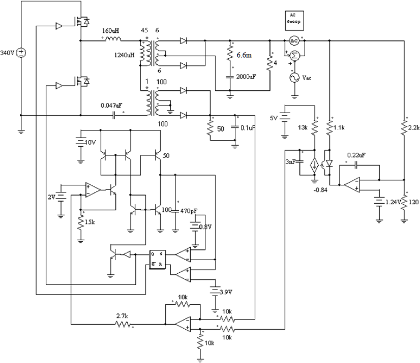
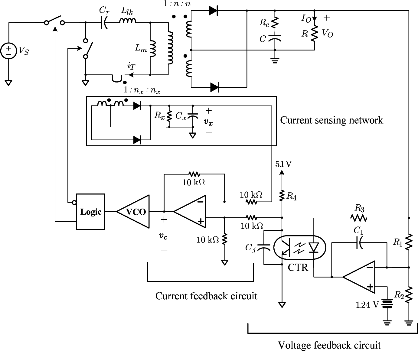
Figure 1 shows the circuit diagram of the experimental LLC converter employing the proposed current mode control. As a typical off-line power supply, the input voltage of the converter is varied between 340 V < VS < 390 V, while the load current is changed between 1 A < IO < 6 A. In addition to an optocoupler-isolated voltage feedback circuit, a current feedback circuit is configured using a center-tapped current transformer and rectifier circuit, in order to exploit the tank current as an integral part of the feedback signal. The functional block in Figure 1 represents the voltage controlled oscillator (VCO). 
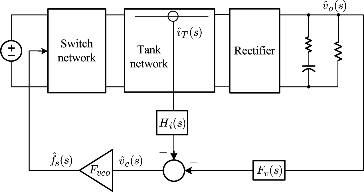
Figure 2 shows a functional block diagram of the current-mode controlled LLC converter. Table 1 shows the expressions and parameters of the gain blocks defined in Figure 2.

2.1. Operational Region

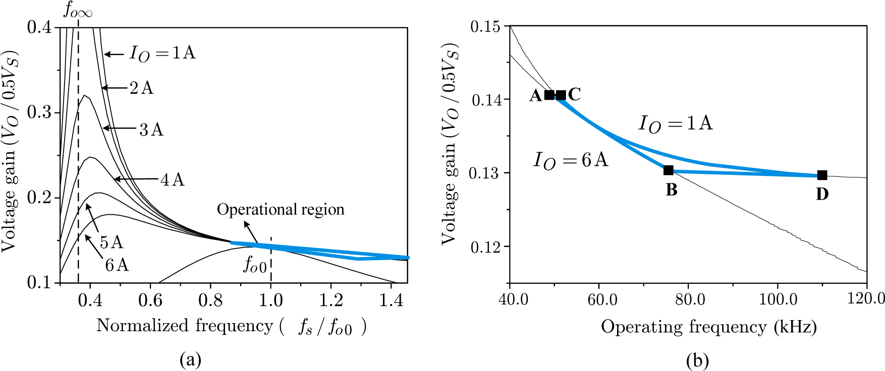
Figure 3a shows a family of the input-to-output curves of the experimental LLC converter, each with a different load condition. The frequency f o 0 = 1 / ( 2 π C R L l k ) denotes the short-circuit resonant frequency of the LLC tank [1]. On the other hand, the frequency f o = 1 / ( 2 π C R ( L l k + L m ) ) is the open-circuit resonant frequency of the LLC tank. For the given input and load specifications, the operational region of the converter can be defined on the voltage gain curves, as highlighted in blue in Figure 3a. Figure 3b shows the expanded view of the operational region in which all the operating points of the LLC converter could locate for the given input and load conditions. On the operational region, the four extreme operating points, Points A, B, C, and D, are shown; Point A: 340 V/6 A, Point B: 390 V/6 A, Point C: 340 V/1 A, and Point D: 390 V/1 A.
For the given LLC converter, the operating point normally lies on the curve between Point A and Point B: VS = 340 390 V with IO = 6 A. Accordingly, the dynamic analysis and control design will be mainly focused on Point A and Point B. Nonetheless, the converter performance will be evaluated for the entire operational region.

2.2. Power Stage Dynamics

The earlier studies [1,2,15] proved that small-signal dynamics of LLC converters vary substantially as operational conditions are altered. The major result of these analyses is shown in 
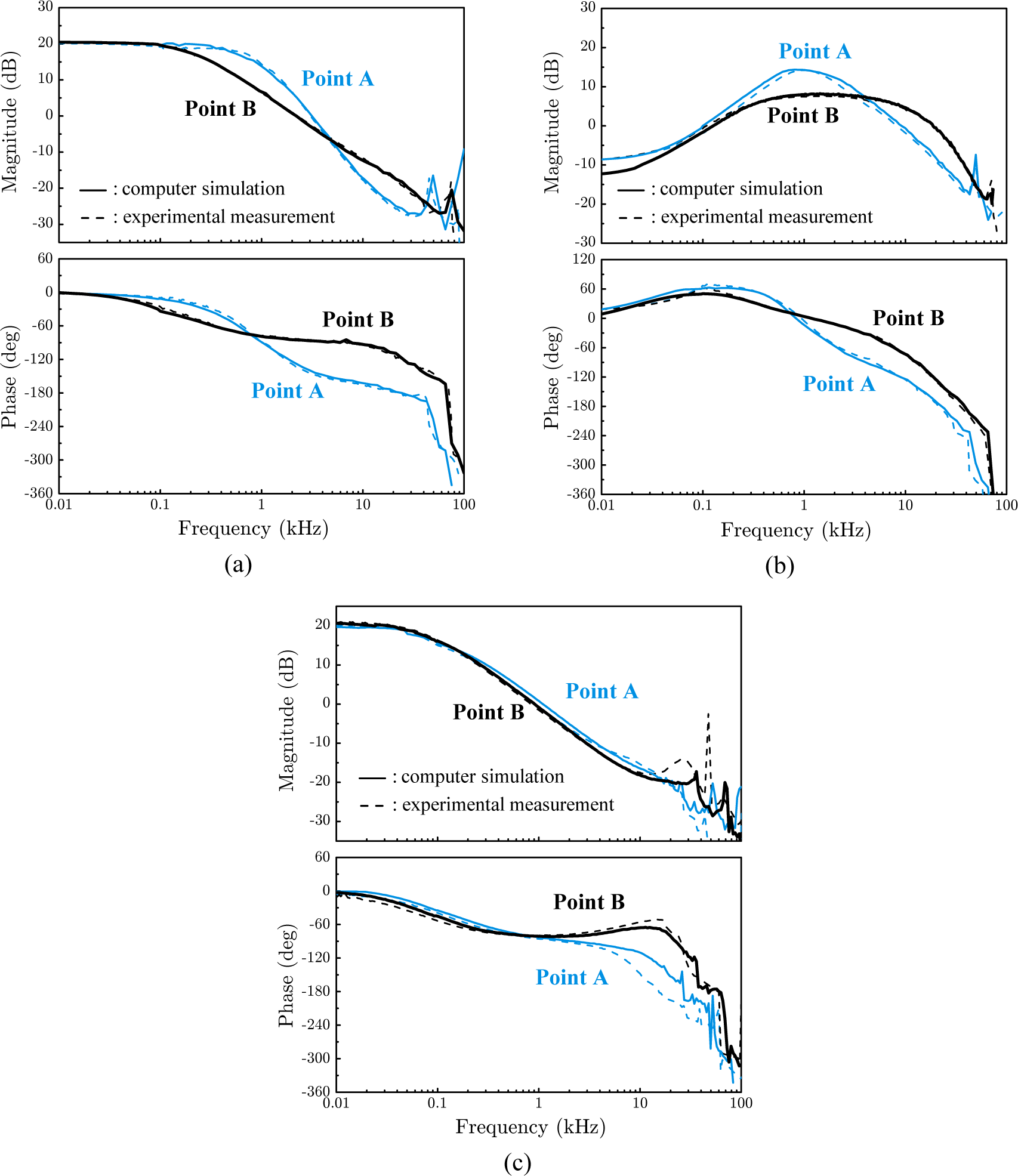
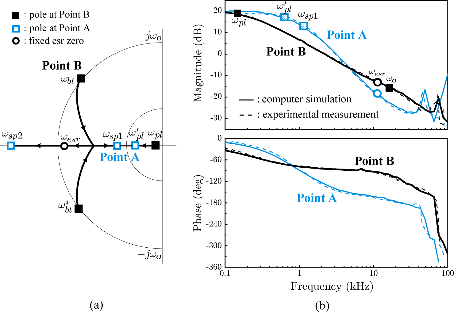
Figure 4 in conjunction with the small-signal dynamics of the experimental LLC converter. Figure 4a depicts the pole/zero trajectory of the frequency-to-output transfer function with respect to the input voltage variation. The trajectory portraits the locations of the poles and zero as the input voltage decreases from VS = 390 V, represented by Point B in Figure 4, to VS = 340 V, denoted as Point A, while delivering the load current of IO = 6 A. Detailed analyses for the locations of poles and zero at Point A and Point B were given in [1,2,15].
The sensitivity of the power stage dynamics can readily be illustrated using the control-to-output transfer function. For this purpose, Figure 4b shows the control-to-output transfer function of the experimental LLC converter, evaluated not employing the proposed resonant tank current feedback. The transfer function is expressed as
G υ c o ( s ) = υ ^ o ( s ) υ ^ c ( s ) = F υ c o υ ^ o ( s ) f ^ s ( s )
where Fvco is the VCO gain and υ ^ o ( s ) / f ^ s ( s ) is the frequency-to-output voltage transfer function. The control-to-output transfer functions Gvco(s), along with all the forthcoming power stage and closed-loop transfer functions, are evaluated at Point A and Point B. In the transfer function analysis, the time-domain simulation method [1,2,15,16] is used for theoretical predictions. Theoretical predictions are then presented in parallel with experimental measurements. The PSIM [17] model used for the time-domain simulation method is given in Appendix.
The transfer function exhibits notable changes, in the exact same manner as predicted from the pole/zero trajectory in Figure 4a. It is observed that Point B has a single pole ωpl at low frequencies and shows the first-order system behavior from low- to mid-frequencies. In contrast, Point A reveals the second-order behavior with rapid-declining phase characteristics due to the two neighboring poles, ω p l and ωsp1. Detailed discussions about the small-signal dynamics are given in [1,2,15].

2.3. Limitation of Conventional Voltage Mode Control

In conventional voltage mode control, the output voltage alone is employed as the feedback signal. Accordingly, Gvco(s) shown in Figure 4b is used as the basis for the voltage feedback design. For this case, the loop gain and other closed-loop transfer functions will be directly affected by the changes in Gvco(s).
One practical design strategy at the presence of wide variations in Gvco(s) is to design the voltage compensation for the worst-case operational condition. Point A exhibits the second-order behavior with unfavorable phase characteristics and thus can be considered as the worst-case condition. As demonstrated in [1], a three-pole two-zero compensation can be employed to achieve stable operation with good dynamic performance at Point A. However, the resulting design becomes overly conservative and offers only limited performance at other operating points than Point A.

3. Principle of Current Mode Control

The basic concept of current mode control is to employ an additional feedback from the tank circuit variable to construct the composite feedback signal that would not be affected by potential changes in power stage dynamics. This aim can be accomplished by adapting the two-loop control scheme [16]. When one tank circuit variable is applied as the inner feedback signal and subsequently mixed with the outer voltage feedback signal, the composite feedback signal will be generated, which will largely remain unaffected by potential drifts in power stage dynamics. The theoretical validation of this statement will be given later in this section.
Among the tank circuit variables, the current waveforms are easier to sense and process than the voltage waveforms. Thus, one of the current waveforms is commonly employed as the second feedback signal in the two-loop control scheme [16]. Any current waveform in the tank circuit can be exploited, as far as it carries the tank circuit dynamics. The possible candidates will be the switch current, diode current, and tank current. In the proposed current mode control, the tank current feedback signal is added to the optocoupler-isolated voltage feedback signal to generate the composite feedback signal. The reasons for this selection are as follows.
  • The switch current is a half sinusoid and should be low-pass filtered to yield a continuous current feedback signal. The half sinusoid requires a low pass filter whose corner frequency is located at lower frequencies. The resulting filter would incur an undesirable low-frequency phase delay to the current feedback signal.
  • The diode current is only available at the secondary side of the transformer. The diode current feedback signal, extracted from the secondary side, should be transmitted to the primary side with isolation. This would complicate the feedback circuit implementation.
  • The tank current is a full sinusoid, which is easier to rectify and filter. Also, the tank current is sensed at the primary side of the transformer and directly mixed with the voltage feedback signal.
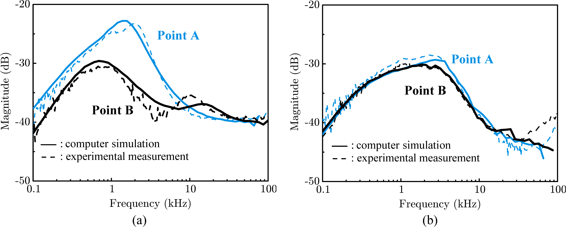
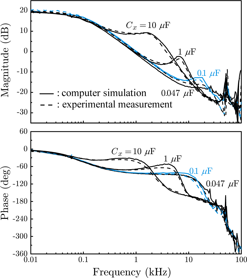
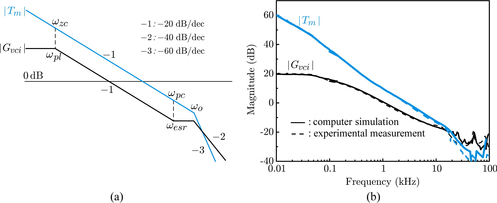
The control-to-output transfer function, evaluated with the resonant tank current feedback, is determined from Figure 2
G υ c i ( s ) = υ ^ o ( s ) υ ^ c ( s ) H i ( s ) 0 = F υ c o υ ^ o ( s ) f ^ s ( s ) 1 + F υ c o i ^ T ( s ) f ^ s ( s ) H i ( s )
where Hi(s) is the transfer function of the current feedback circuit and i ^ T ( s ) / f ^ s ( s ) is the frequency-to-tank current transfer function. Equation (2) is approximated to
G υ c i ( s ) F υ c o υ ^ o ( s ) f ^ s ( s ) F υ c o i ^ T ( s ) f ^ s ( s ) H i ( s )
assuming the condition F υ c o | i ^ T ( s ) / f ^ s ( s ) | | H i ( s ) | 1, which is true over most frequency range of practical importance. Figure 5 shows the Bode plots of the transfer functions involved with Equation (3). Figure 5a shows the numerator of Equation (3), which corresponds to the control-to-output transfer function, G υ c o ( s ) = F υ c o υ ^ o ( s ) / f ^ s ( s ), in case of the conventional voltage mode control. Figure 5b shows the denominator of Equation (3), which corresponds to the gain of the inner current loop created by the tank current feedback. While Figure 5b shows wide variations at the two different operating points, it can be observed that the transition pattern of Figure 5b closely resembles the transition pattern of Figure 5a. This is because any drift in power stage dynamics will commonly propagate into both υ ^ o ( s ) / f ^ s ( s ) and i ^ T ( s ) / f ^ s ( s ) and therefore will exert the same influence on the numerator and denominator of Equation (3). Accordingly, the consequential effects of any changes in power stage dynamics will be canceled each other in Equation (3) and the control-to-output transfer function will remain mostly invariant.
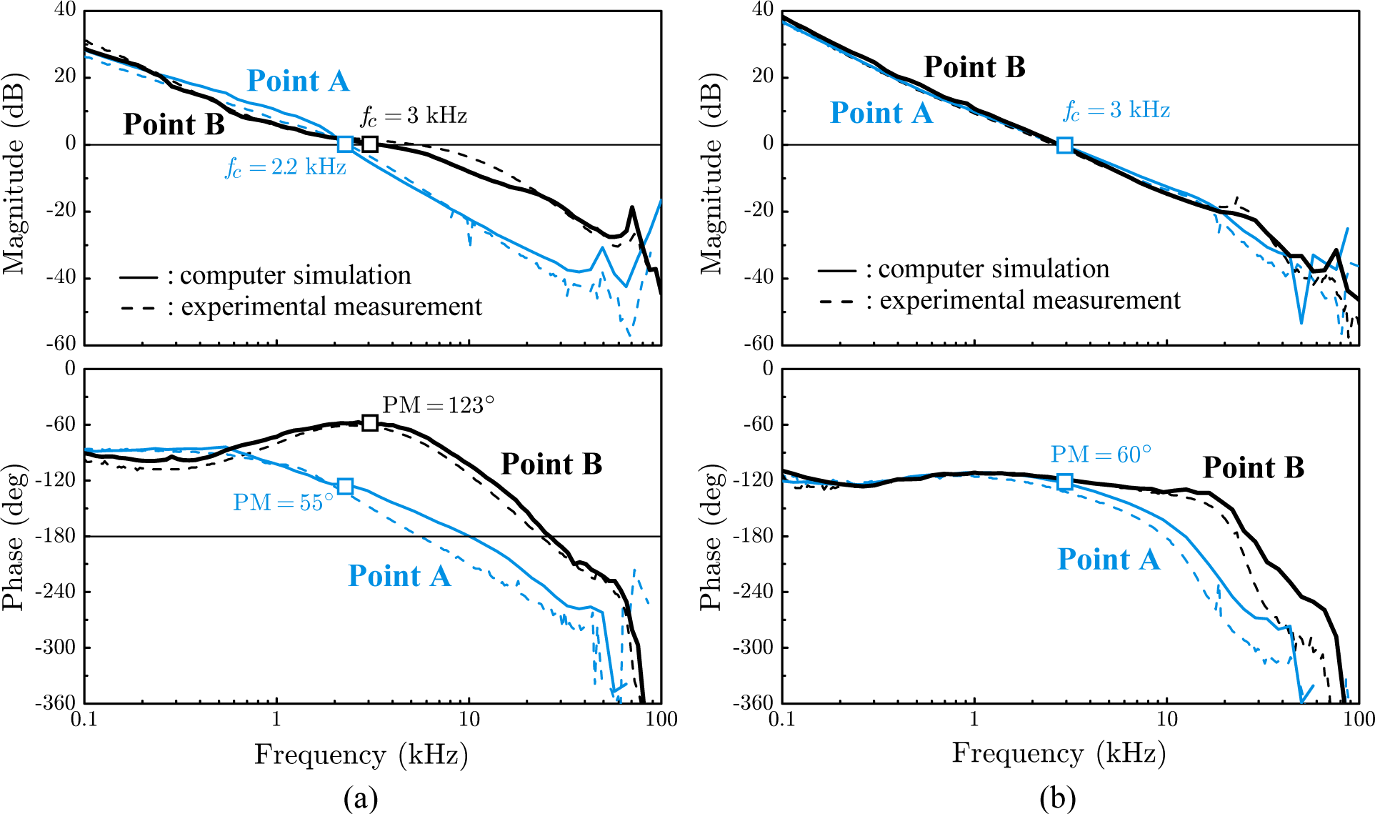
Figure 5c shows the control-to-output transfer function at the two different operating points. The experimental magnitude plot at Point B shows a peaking at the frequency near 75 kHz. This frequency corresponds to the switching frequency of the prototype converter at Point B, as demonstrated in Figure 3b. The switching noise produced the peaking in the magnitude measurement. The transfer function indeed shows consistent characteristics for wide frequency range. The benefit of the tank current feedback is clearly seen when Figure 5c is compared with Figure 5a. The control-to-output transfer function remains mostly unchanged for wide frequency range and the voltage feedback compensation thus can be designed for optimal performance for the entire operational range.

4. Design of Current Mode Control

The implementation of the proposed current mode control requires the design of both the current feedback circuit and voltage feedback compensation.

4.1. Current Feedback Circuit Design

Due to the presence of the rectifier circuit, the current feedback circuit presents a first-order low pass filter transfer function
H i ( s ) = K i 1 + s ω p i
with
K i = R x n x
and
ω p i = 1 R x C x
where nx is the turns ratio of current transformer, Rx is the resistance, and Cx is the capacitance of the rectifier circuit. The dc gain Ki can be selected considering the magnitude of the tank current. For the prototype converter, the dc gain is set at Ki = 0.5 with nx = 100 and Rx = 50 Ω.
The pole frequency ωpi should be selected to obtain sufficient filtering, while not causing any detrimental effects to the control-to-output transfer function. Figure 6 shows Gvci(s) evaluated at Point A using four different values for Cx with the predetermined Rx = 50 Ω. The transfer function exhibits a resonant-type peaking whose frequency is inversely proportional to the capacitance Cx. For larger capacitances, the peaking occurs at low frequencies, thereby deteriorating the mid-frequency phase characteristics. On the other hand, small capacitances push the peaking towards higher frequencies and do not significantly change the control-to-output transfer function. It was found that Cx = 0.1 µF pushes the peaking out of the control bandwidth.
A further decrease in Cx will worsen the filtering characteristics of the rectifier circuit. Figure 7 shows the tank current feedback signal, vx in Figure 1, and the composite feedback signal, vc in Figure 1, measured with Cx = 0.1 µF and with Cx = 0.047 µF at the operating Point A. Figure 7a illustrates the waveforms with Cx = 0.1 µF. The tank current feedback signal contains a finite ripple component due to the nonideal filtering characteristics of the rectifier circuit. Furthermore, the ripple component shows cycle-by-cycle imbalance due to the mismatch in the inductive parameters of the center-tapped transformers, used in the resonant tank circuit and in the current sensing circuit. Nonetheless, the composite feedback signal maintains a sufficient integrity due to a large DC offset contained in the voltage feedback signal. Figure 7b shows the waveforms with Cx = 0.047 µF. With a smaller capacitance, both the ripple component and imbalance are increased, thus jeopardizing the proper operation of the controller. Based on this trade-off study, Cx = 0.1 µF is finally selected for the experimental LLC converter.

4.2. Voltage Feedback Compensation Design

In order to design the voltage feedback circuit, it might be necessary to find an exact expression for the control-to-output transfer function Gvci(s), evaluated at the presence of the tank current feedback. However, this task will be overly challenging due to the complex power stage dynamics. As an alternative engineering practice, Gvci(s) can be approximated as a third-order polynomial, based on the general profile of the Bode plots in Figures 5c and 6.
G υ c i ( s ) = K υ c i 1 + s ω e s r ( 1 + s ω p l ) ( 1 + s Q ω o + s 2 ω o 2 )
The zero frequency ωesr = 1/(CRc) is determined by the equivalent series resistance (ESR) and capacitance of the output filter capacitor. The pole frequency ωpl usually appears at lower frequencies. As shown in Figures 5c and 6, this low frequency pole emerges at a fixed frequency, regardless of changes in operational conditions. From Figures 5c and Figure 6, the location of this pole is approximated as ωpl 2π 330 rad/s.
For the given the control-to-output transfer function structure, a two-pole one-zero compensation
F υ ( s ) = K υ s 1 + s ω z c 1 + s ω p c
would provide desirable loop gain characteristics. Figure 8a shows the construction of the asymptotic loop gain plot, |Tm| = |GvciFv|, with assumptions ωzc = ωpl and ωpc = ωesr. The compensation zero is selected at ωzc = 2 × 10³ rad/s, while the compensation pole is set at ωpc = 7.5 × 10⁴ rad/s. The integrator gain is designed as Kv = 7.0×10³ to place the loop gain crossover at higher frequencies, while securing a sufficient phase margin. Using the selected compensation parameters, the circuit components for the voltage feedback circuit are determined as shown in Figure 1.
Figure 8b shows the theoretical and experimental plots for |Gvci| and |Tm| of the experimental LLC converter operating at Point A. This figure validates the theoretical design procedure shown in Figure 8a.

5. Performance of Current Mode Control

This section presents the performance of the proposed current mode control, in comparison with that of the conventional voltage mode control. The voltage mode control is duly designed using a three-pole two-zero compensation, based on the design procedures proposed in [1].

5.1. Loop Gain Characteristics

Figure 9 illustrates the measured and simulated loop gains of the experimental LLC converter with both the voltage mode control and current mode control. As predicted in Section 2.3, the loop gain of the voltage mode control is directly affected by the changes in the control-to-output transfer function and shows considerable variations at the two different operating points. In contrast, the current mode control maintains desirable loop gain characteristics with minimal changes in both the crossover frequency and phase margin. With the proposed current mode control design, the loop gain crosses the 0 dB line at 2π 3.0 × 10³ rad/s with a 60° the phase margin at both Point A and Point B.

5.2. Output Impedance

Figure 10 depicts the measured and simulated output impedances of the experimental LLC converter with the two different control schemes. The output impedance with the voltage mode control shows substantial drifts between Point A and Point B. At Point A, the output impedance shows a large peak of 22 dB. On the other hand, the current mode control shows near-uniform output impedance characteristics at both Point A and Point B. Here, the peak value of the output impedance is limited by 30 dB.

5.3. Step Load Response

Figure 11 shows the measured step load transient response waveforms of the voltage mode control and proposed current mode control. The step load transient waveforms at Point A, where the voltage mode control shows the inferior loop gain and output impedance characteristics, are shown in Figure 11. For both the voltage mode control and current mode control, the step changes of IO = 6 A 1 A 6 A are introduced, while the input voltage is fixed at VS = 340 V. As expected from the output impedance analysis, the current mode control shows superior transient behavior in both the tank current iT and output voltage vO, thereby highlighting the merit of the proposed current mode control.

6. Conclusions

This paper proposed a new current mode control scheme for LLC series resonant DC-to-DC converters. Using the additional feedback from the resonant tank current, the proposed control scheme effectively nullifies the consequential effects of possible changes in power stage dynamics, and therefore consistently provides desired closed-loop performance for the entire operational range of 340 V < VS < 390 V and 1 A < IO < 6 A.
The new current mode control outperformed the conventional voltage mode control and offered nearly the same loop gain characteristics and output impedance characteristics at the two extreme operating points. In addition, current mode control provided some improvements in the step load response. This signifies that the converter always retains the improved performance, as far as it remains in the given operational region.
This paper presented the design guidelines for the proposed current mode control scheme. The procedures for both the current feedback circuit design and voltage feedback compensation are formulated. While the LLC series resonant converter is considered in the paper, the proposed control scheme can be adapted to all types of resonant power converters as a viable substitute for the conventional voltage mode control that provides only limited performance.

Acknowledgments

This research was supported in part by the MSIP (Ministry of Science, ICT & Future Planning), Korea, under the ITRC (Information Technology Research Center) support program (IITP-2015-H8501-15-1006) supervised by the IITP (Institute for Information & communications Technology Promotion) and in part by Kyungpook National University Reserach Fund, 2012.

Author Contributions

Jinhaeng Jang and Syam Kumar Pidaparthy jointly produced experimental data, prepared computer simulations, figures, and tables, and wrote the draft of the paper. Byungcho Choi supervised the research and finalized the paper.

Conflicts of Interest

The authors declare no conflict of interest.

Appendix

Figure A1 shows the circuit diagram of the PSIM model [17] used for time-domain simulations to extract the loop gain characteristics of the experimental LLC converter.
Figure A1. PSIM model for the loop gain analysis of current mode control of LLC series resonant converter.
Energies 08 06098f12

References

  1. Jang, J.; Joung, M.; Choi, B.; Hong, S.; Lee, S. Dynamic analysis and control design of optocoupler-isolated LLC series resonant converters with wide input and load variations. IET Power Electron 2012, 5, 755–764. [Google Scholar]
  2. Yang, B. Topology Investigation for Front End DC/DC Power Conversion for Distributed Power System. Ph.D. Thesis, Virginia Polytechnic Institute and State University, Blacksburg, VA, USA, 2003. [Google Scholar]
  3. Han, J.H.; Lim, Y.C. Design of an LLC resonant converter for driving multiple LED lights using current balancing of capacitor and transformer. Energies 2015, 8, 2125–2144. [Google Scholar]
  4. Musavi, F.; Craciun, M.; Gautam, D.; Eberle, W.; Dunford, W. An LLC resonant DC-DC converter for wide output voltage range battery charging applications. IEEE Trans. Power Electron 2013, 28, 5437–5445. [Google Scholar]
  5. Musavi, F.; Craciun, M.; Gautam, D.; Eberle, W. Control strategies for wide output voltage range LLC resonant DC-DC converters in battery chargers. IEEE Trans. Veh. Technol 2014, 63, 1117–1125. [Google Scholar]
  6. Fang, Z.; Cai, T.; Duan, S.; Chen, C. Optimal design methodology for LLC resonant converter in battery charging applications based on time-weighted average efficiency. IEEE Trans. Power Electron 2014, 30, 5469–5483. [Google Scholar]
  7. Ryu, M.; Kim, H.; Baek, J.; Kim, H.; Jung, J. Effective test bed of 380-V DC distribution system using isolated power converters. IEEE Trans. Ind. Electron 2015, 62, 4525–4536. [Google Scholar]
  8. Kuo, M.T.; Tsou, M.C. Simulation of standby efficiency improvement for a line level control resonant converter based on solar power systems. Energies 2015, 8, 338–355. [Google Scholar]
  9. Yang, G.; Dubus, P.; Sadarnac, D. Double-phase high-efficiency, wide load range high-voltage/low-voltage LLC DC/DC converter for electric/hybrid vehicles. IEEE Trans. Power Electron 2015, 30, 1876–1886. [Google Scholar]
  10. Buccella, C.; Cecati, C.; Latafat, H.; Pepe, P.; Razi, K. Observer-based control of LLC DC/DC resonant converter using extended describing functions. IEEE Trans. Power Electron 2014, 30, 5881–5891. [Google Scholar]
  11. Feng, W.; Lee, F.; Mattavelli, P. Optimal trajectory control of LLC resonant converters for LED PWM dimming. IEEE Trans. Power Electron 2014, 29, 979–987. [Google Scholar]
  12. Feng, W.; Lee, F.; Mattavelli, P. Simplified optimal trajectory control (SOTC) for LLC resonant converters. IEEE Trans. Power Electron 2013, 28, 2415–2426. [Google Scholar]
  13. Zong, S.; Luo, H.; Li, W.; He, X.; Xia, C. Theoretical evaluation of stability improvement brought by resonant current loop for paralleled LLC converters. IEEE Trans. Ind. Electron 2015, 62, 4170–4180. [Google Scholar]
  14. Li, H.Y.; Li, X.; Lu, M.; Hu, S. A linearized large signal model of an LCL-type resonant converter. Energies 2015, 8, 1848–1864. [Google Scholar]
  15. Yang, B.; Lee, F.C.; Jovanovic, M. Small-signal analysis for LLC resonant converter. CPES Semin 2003, 7, 144–149. [Google Scholar]
  16. Choi, B. Pulsewidth Modulated DC-to-DC Power Conversion: Circuits, Dynamics, and Control Designs; John Wiley & Sons: Hoboken, NJ, USA, 2013. [Google Scholar]
  17. Powersim Inc. PSIM User’s Guide, version 9.0 ed; Powersim Inc: Rockville, MD, USA, 2010. [Google Scholar]
Figure 1. Experimental LLC converter with proposed current mode control: VS = 340 390 V, VO = 24 V, IO = 1 6 A, Cr = 47 nF, Llk = 160 µH, Lm = 1.24 mH, n = 0.14, C = 2 mF, Rc = 6.6 mΩ, nx = 100, Rx = 50 Ω, Cx = 0.1 µF, R1 = 2.2 kΩ, R2 = 120 Ω, R3 = 1.1 kΩ, R4 = 13 kΩ, C1 = 0.22 µF. The functional block VCO represents the voltage controlled oscillator, CTR = 0.84 is the current transfer ratio of the optocoupler, and Cj = 3 nF is the junction capacitor of the optocoupler.
Energies 08 06098f1
Figure 2. Functional block diagram of current-mode controlled LLC converter. Fvco is voltage controlled oscillator (VCO) gain and Hi(s) is the transfer function of the current feedback circuit, and Fv(s) is the feedback compensation of the voltage feedback circuit.
Energies 08 06098f2
Figure 3. Input-to-output voltage gain curves and operational region of experimental LLC converter. (a) Input-to-output voltage gain curves: fo0 58 kHz and fo∞ 20 kHz; (b) Expanded view of operational region.
Energies 08 06098f3
Figure 4. Power stage dynamics of experimental LLC converter. (a) Pole/zero trajectory of frequency-to-output transfer function; (b) Experimental Bode plot of control-to-output transfer function G υ c o : ω o = | ω b t | = | ω b t * |.
Energies 08 06098f4
Figure 5. Power stage transfer functions of experimental LLC converter. (a) Numerator of Equation (3); (b) Denominator of Equation (3); (c) Control-to-output transfer function Gvci(s) with current mode control.
Energies 08 06098f5
Figure 6. Control-to-output transfer function with different filter capacitance.
Energies 08 06098f6
Figure 7. Current feedback signal, vx, and composite feedback signal, vc, with Cx = 0.1 µF and Cx = 0.047 µF. (a) Cx = 0.1 µF; (b) Cx = 0.047 µF.
Energies 08 06098f7
Figure 8. Voltage feedback compensation design. (a) Design strategy. (b) Design verification.
Energies 08 06098f8
Figure 9. Loop gain characteristics of voltage mode control and proposed current mode control. (a) Voltage mode control; (b) Current mode control.
Energies 08 06098f9
Figure 10. Output Impedance of voltage mode control and proposed current mode control. (a) Voltage mode control; (b) Current mode control.
Energies 08 06098f10
Figure 11. Step-load transient response waveforms of voltage mode control and proposed current mode control. (a) Voltage mode control; (b) Current mode control.
Energies 08 06098f11
Table 1. Expressions for Gain Blocks in Figure 2.
Fυco2π · 6.9 × 104
Hi(s) R x n x 1 1 + s C x R x = 0.5 1 + s 2.0 × 10 5
Fυ(s) CTR R 4 s C 1 R 1 R 3 1 + s C 1 R 1 1 + s C j R 4 = 7 × 10 3 ( 1 + s 2 × 10 3 ) s ( 1 + s 7.5 × 10 4 )

