
An Integrated Chip High-Voltage Power Receiver for Wireless Biomedical Implants

Abstract
:1. Introduction
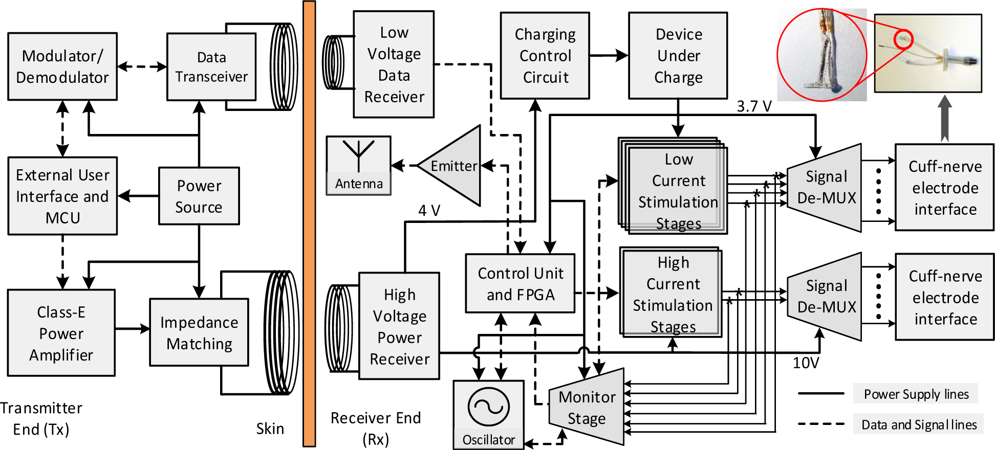
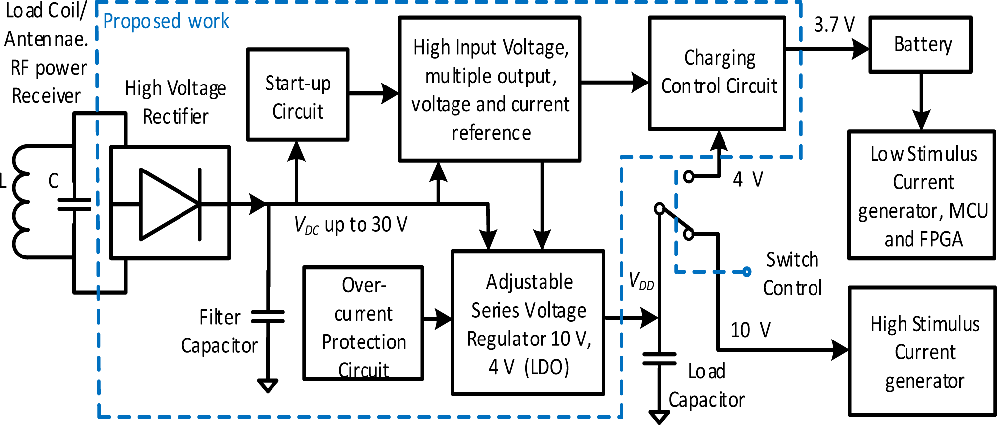
2. Architectural Overview of the System
3. Design Approach and System Specification
3.1. Implementation Method
3.2. Design Specification
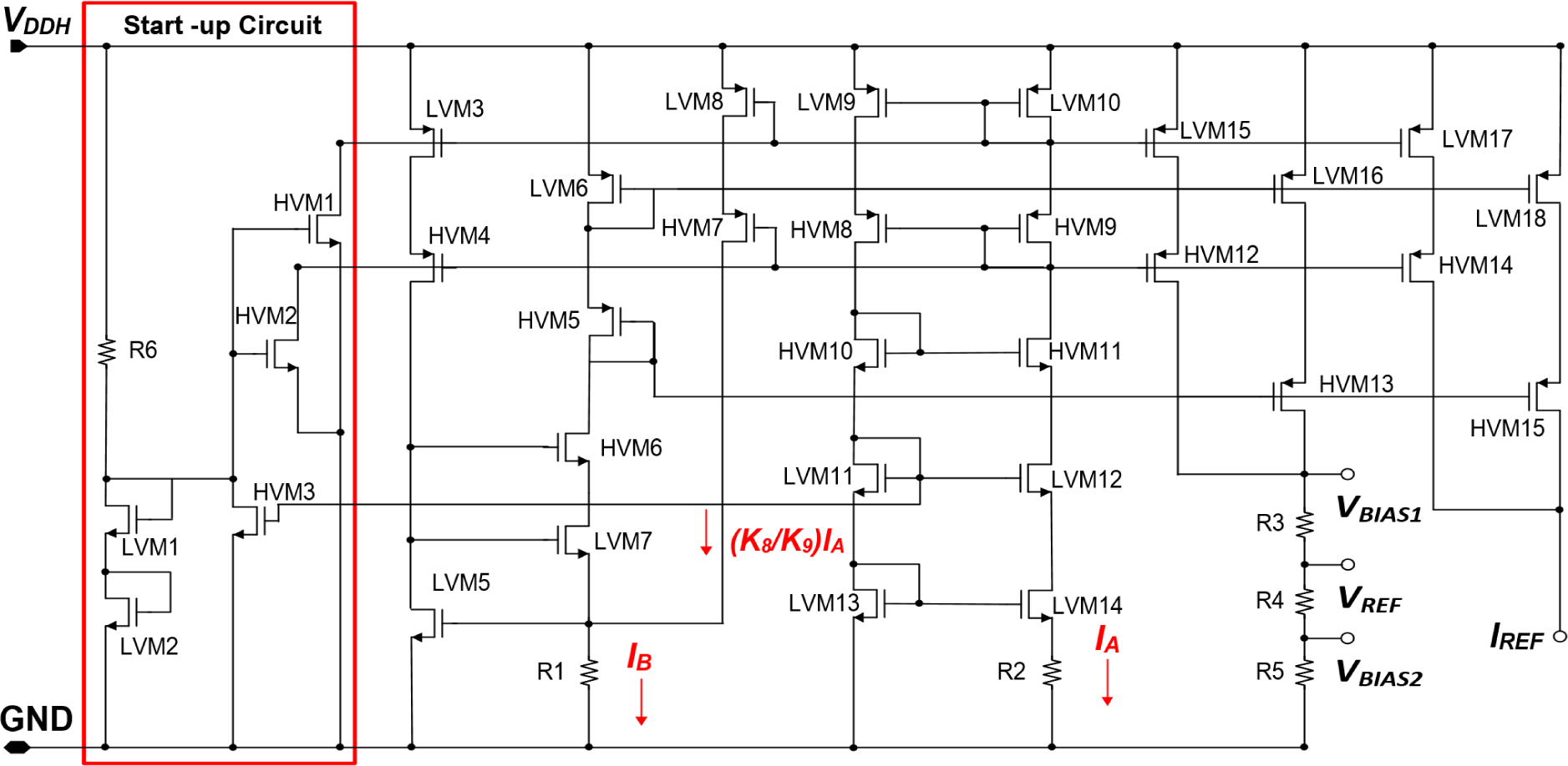
4. Circuit Design Methodology
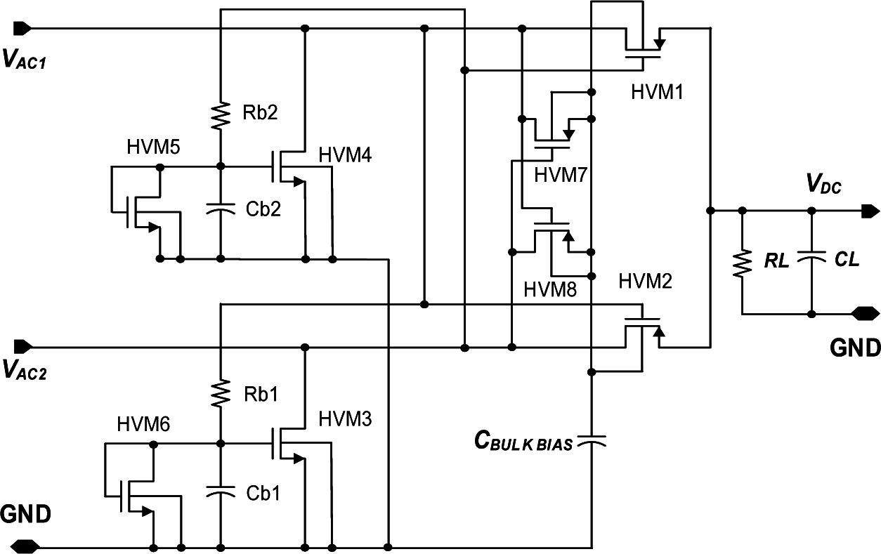
4.1. High-Voltage Bridge Rectifier
4.2. High-Voltage Reference and Bias Current Generator
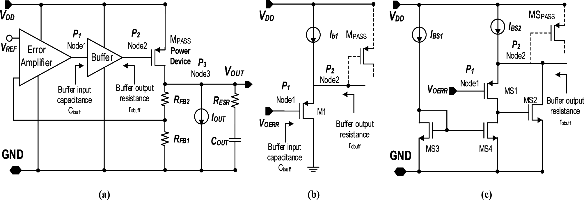
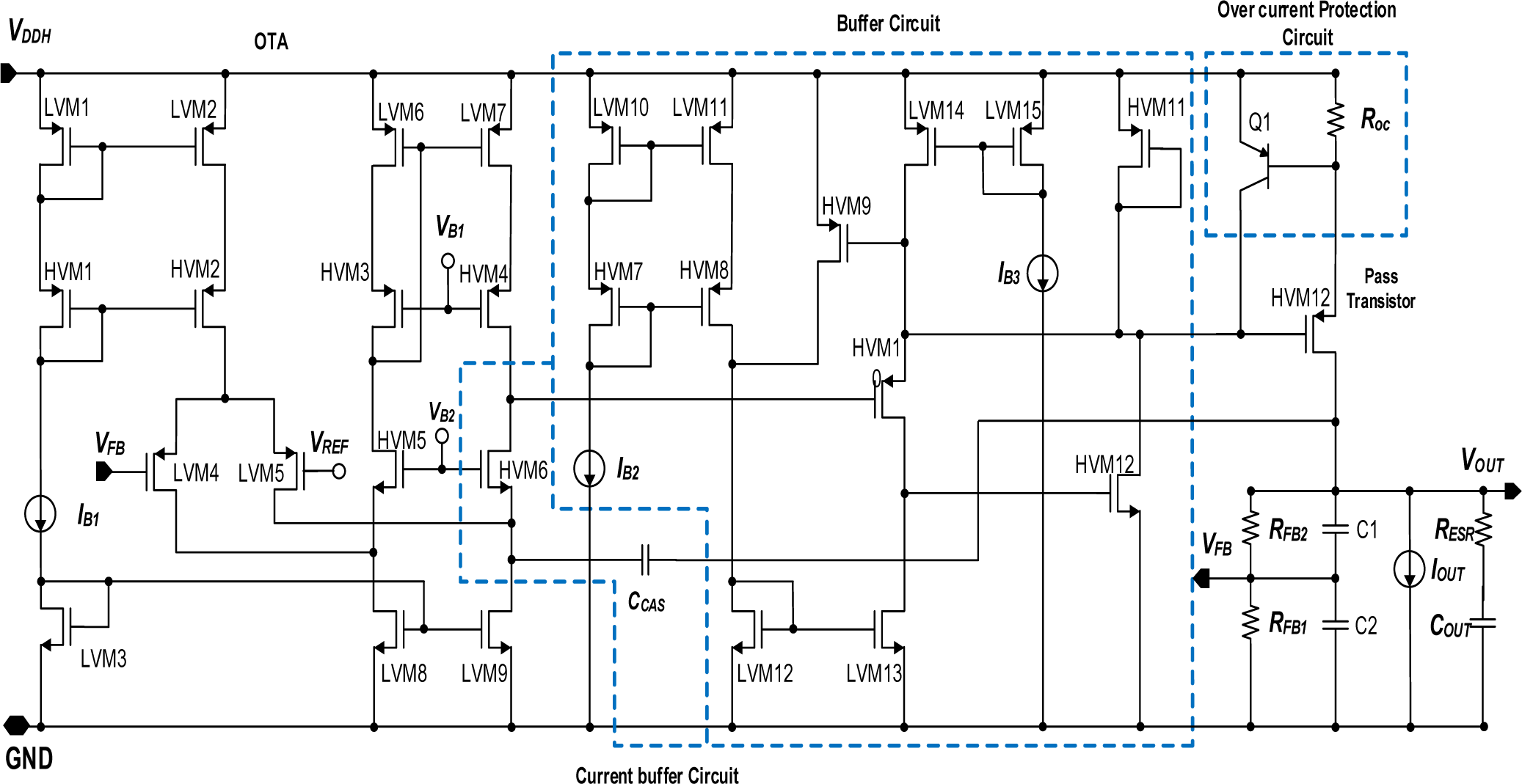
4.3. High Input Voltage Linear Regulator
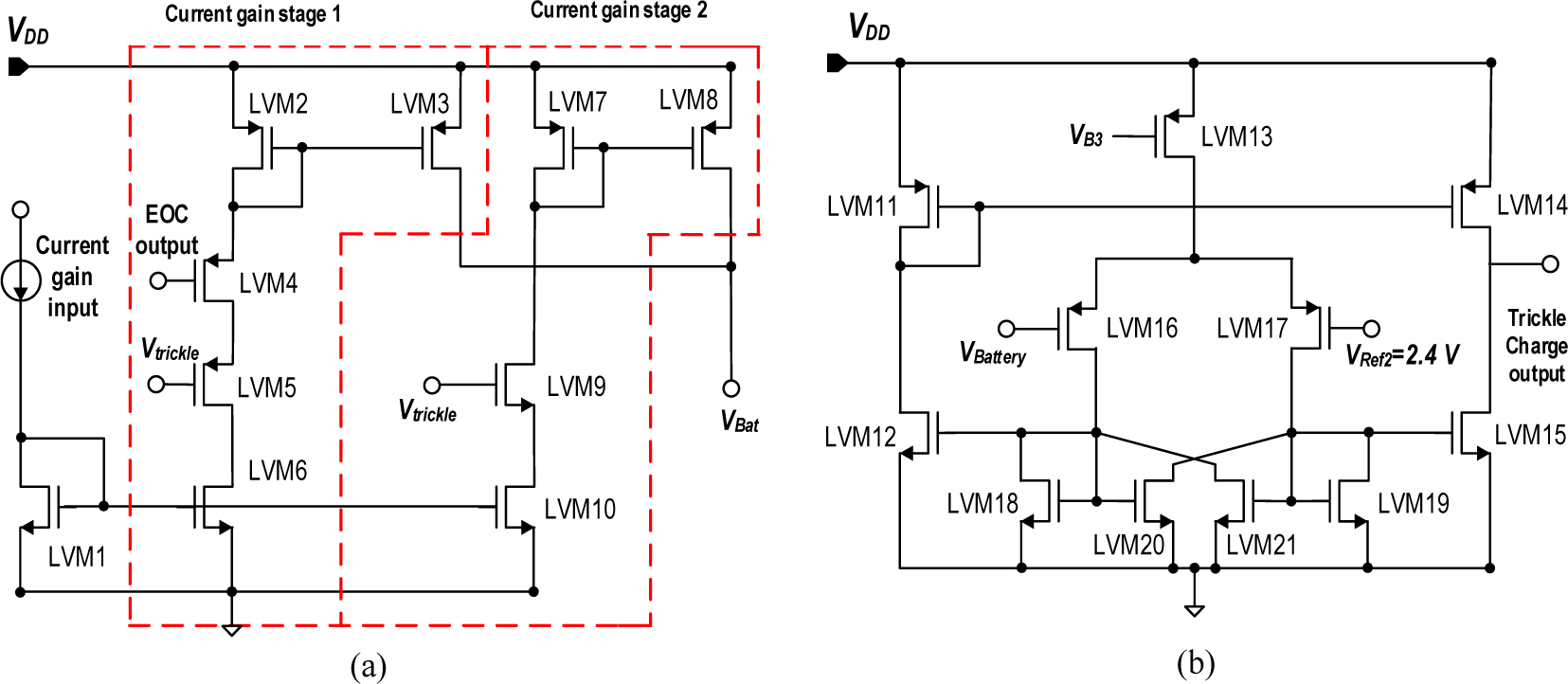
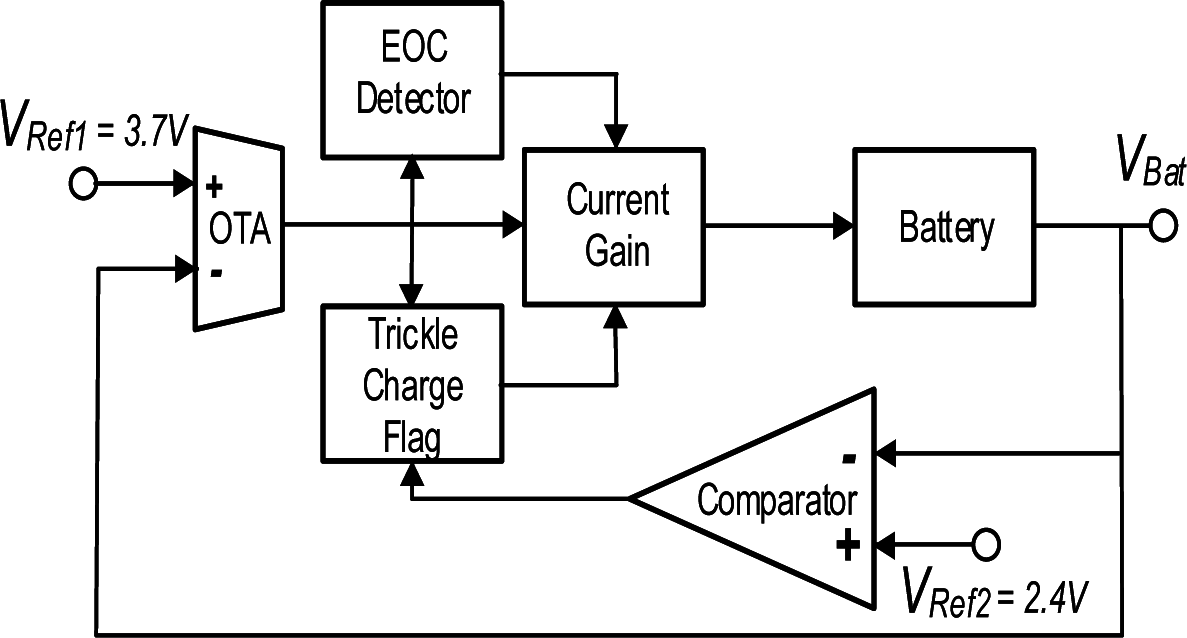
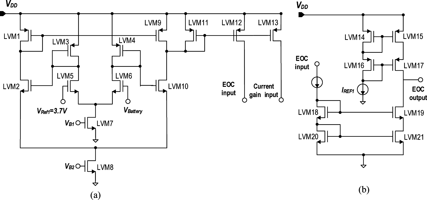
4.4. Battery Charger Circuit
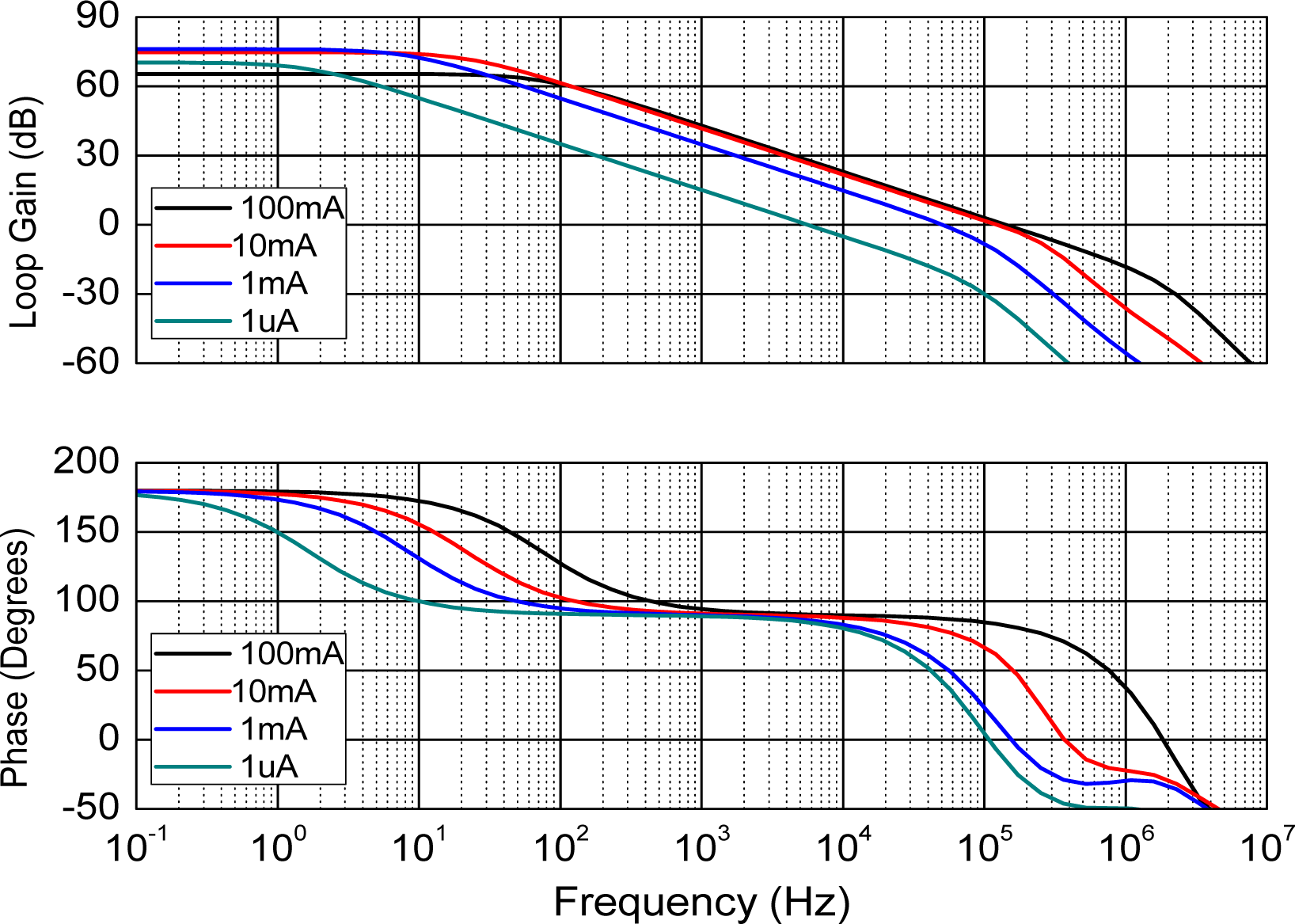
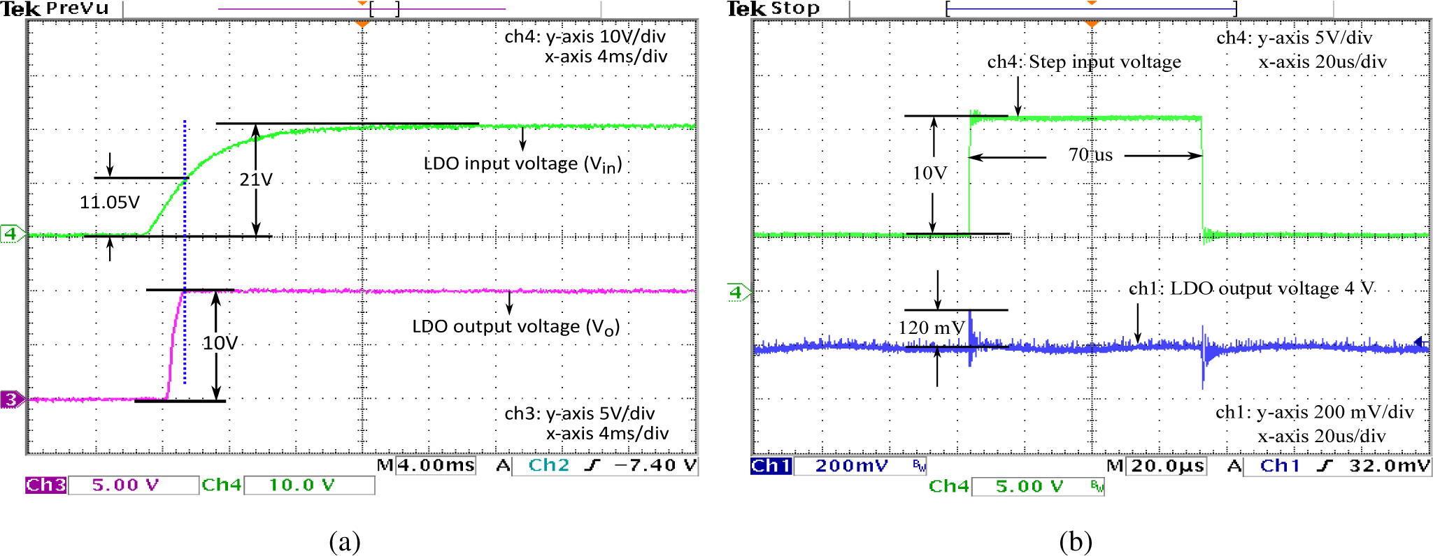
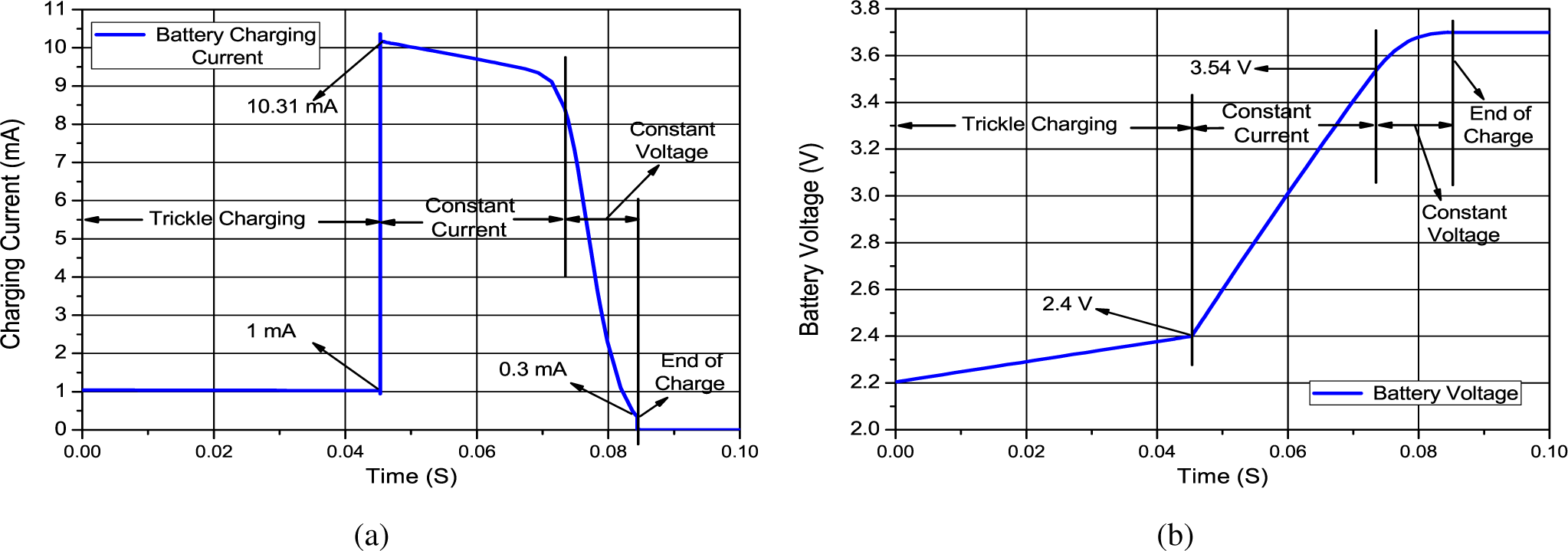
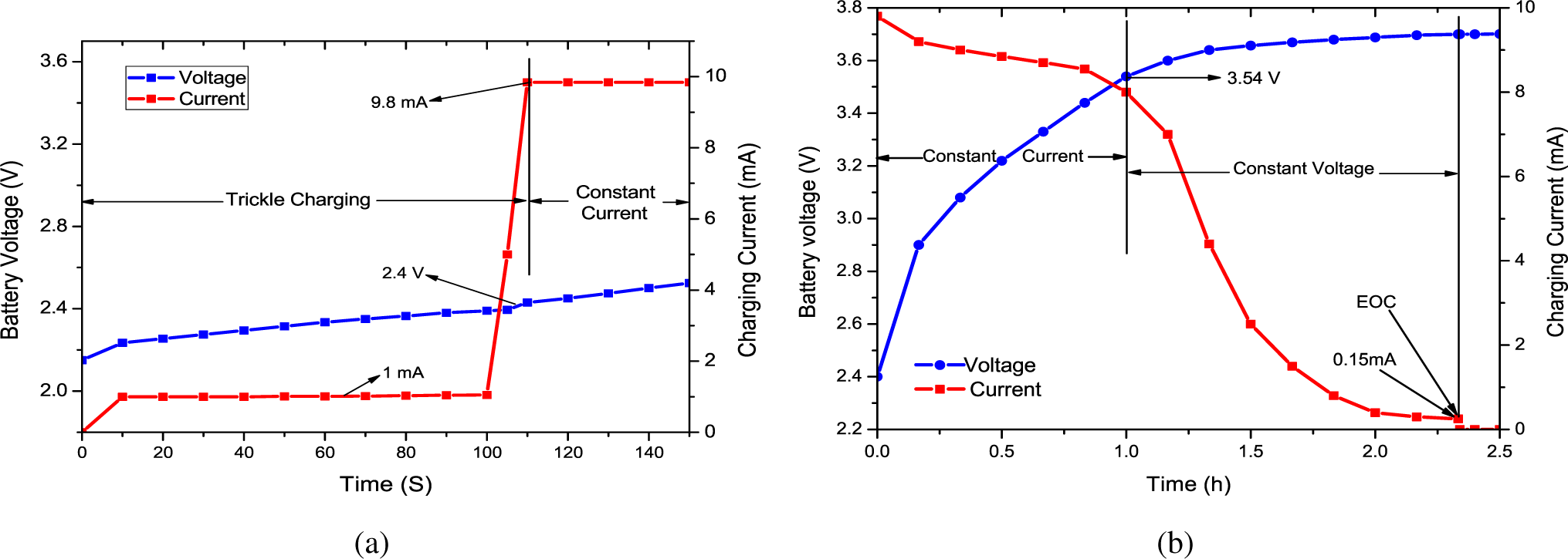
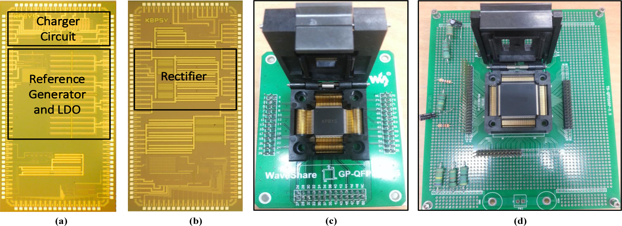
5. Simulation and Experimental Results
6. Conclusions
Acknowledgments
Author Contributions
Conflicts of Interest
References
- Guo, S.; Lee, H. An Effiency-Enhanced CMOS Rectifier With Unbalanced-Biased Comparators for Transcutaneous-Powered High-Current Implants. IEEE J. Solid-State Circuits 2009, 44, 1796–1804. [Google Scholar]
- Lee, H.M.; Ghovanloo, M. An Integrated Power-Efficient Active Rectifier With Offset-Controlled High Speed Comparators for Inductively Powered Applications. IEEE Trans. Circuits Syst. I Regul. Papers 2011, 58, 1749–1760. [Google Scholar]
- Mounaim, F.; Sawan, M. Integrated High-Voltage Inductive Power and Data-Recovery Front End Dedicated to Implantable Devices. IEEE Trans. Biomed. Circuits Syst. 2011, 5, 283–291. [Google Scholar]
- Li, Y.T.; Peng, C.W.; Chen, L.T.; Lin, W.S.; Chu, C.H.; Chen, J.J.J. Application of Implantable Wireless Biomicrosystem for Monitoring Nerve Impedance of Rat After Sciatic Nerve Injury. IEEE Trans. Neural Syst. Rehabil. Eng. 2013, 1, 121–128. [Google Scholar]
- Li, Y.T.; Chang, C.H.; Chen, J.J.J.; Wang, C.C.; Liang, C.K. Development of Implantable Wireless Biomicrosystem for Measuring Electrode-Tissue Impedance. J. Med. Biol. Eng. 2005, 25, 99–105. [Google Scholar]
- Chiu, H.W.; Chuang, J.M.; Lu, C.C.; Lin, W.T.; Lin, C.W.; Lin, M.L. In Situ Measurement of Tissue Impedance Using an Inductive Coupling Interface Circuit. IEEE Trans. Biomed. Circuits Syst. 2013, 7, 225–235. [Google Scholar]
- Daza, P.; Olmo, A.; Canete, D.; Yufera, A. Monitoring living cell assays with bio-impedance sensors. Sens. Actuators B Chem. 2013, 176, 605–610. [Google Scholar]
- Balachandran, G.; Barnett, R. A 110 nA Voltage Regulator System With Dynamic Bandwidth Boosting for RFID Systems. IEEE J. Solid-State Circuits 2006, 41, 2019–2028. [Google Scholar]
- Cha, H.K.; Je, M. A single-input dual-output 13.56 MHz CMOS AC-DC converter with comparator-driven rectifiers for implantable devices. Microelectron. J. 2014, 45, 277–281. [Google Scholar]
- Su, C.; Islam, S.K.; Zhu, K.; Zuo, L. A high-temperature, high-voltage, fast response linear voltage regulator. Analog Integr. Circuits Signal Process 2012, 72, 405–417. [Google Scholar]
- Wang, G.; Liu, W.; Sivaprakasam, M.; Kendir, G.A. Design and Analysis of an Adaptive Transcutaneous Power Telemetry for Biomedical Implants. IEEE Trans. Cicuits Syst. 1 2005, 52, 2109–2117. [Google Scholar]
- Kelly, S.; Wyatt, J. A Power-Efficient Neural Tissue Stimulator With Energy Recovery. IEEE Trans. Biomed. Circuits Syst. 2011, 5, 20–29. [Google Scholar]
- Mounaim, F.; Sawan, M. New Neurostimulation Strategy and Corresponding Implantable Device to Enhance Bladder Functions, Biomedical Engineering Trends in Electronics Communications and Software; InTech: Rijeka, Croatia, 2011. [Google Scholar]
- Vijayakuamran Nair, V.; Youn, J.; Choi, J.R. High Voltage Integrated Chip Power Recovering Topology for Implantable Wireless Biomedical Devices, Proceedings of the International Conference on Biomedical Electronics and Devices, BIODEVICES 2015, Lisbon, Portugal, 12–15 January 2015.
- Nicolson, S.; Phang, K. Step-up Versus Step-down DC/DC Converters for RF-Powered Systems, Proceedings of the 2004 International Symposium on Circuits and Systems, 23–26 May 2004; Vancouver, Canada; 5, pp. V900–V903.
- Mounaim, F.; Sawan, M. Toward A Fully Integrated Neurostimulator with Inductive Power Recovery Front-End. IEEE Trans. Biomed. Circuits Syst. 2012, 6, 309–318. [Google Scholar]
- Tomita, K.; Shinoda, R.; Kuroda, T.; Ishikuro, H. 1-W 3.3–16.3-V Boosting Wireless Power Transfer Circuits With Vector Summing Power Controller. IEEE J. Solid-State Circuits 2012, 47, 2576–2585. [Google Scholar]
- Lo, Y.K.; Chen, K.; Gad, P.; Liu, W. A Fully-Integrated High-Compliance Voltage SoC for Epi-Retinal and Neural Prostheses. IEEE Trans. Biomed. Circuits Syst. 2014, 7, 761–772. [Google Scholar]
- Vijayakumaran Nair, V.; Nagakarthik, T.; Choi, J.R. Efficiency Enhanced Magnetic Resonance Wireless Power Transfer system and High Voltage Integrated Chip Power Recovery Scheme, Proceedings of the IEEE International Conference on Electronics, Computing and Communication Technologies (CONECCT), Bangalore, India, 6–7 January 2014; pp. 1–6.
- Nakamoto, H.; Yamazaki, D.; Yamamoto, T.; Kurata, H.; Yamada, S.; Mukaida, K.; Ninomiya, T.; Ohkawa, T.; Masui, S.; Gotoh, K. A Passive UHF RF idetification CMOS Tag IC Using Ferroelectric RAM in 0.35-um Technology. IEEE J. Solid-State Circuits 2007, 42, 101–110. [Google Scholar]
- Mandal, S.; Sarpeshkar, R. Low-Power CMOS Rectifier Design for RFID Applications. IEEE Trans. Circuits Syst. I Regul. Papers 2007, 54, 1177–1188. [Google Scholar]
- Wong, S.Y.; Chen, C. Power efficient multi-stage CMOS rectifier design for UHF RFID tags. Integr. VLSI J. 2011, 44, 242–255. [Google Scholar]
- Cha, H.K.; Park, W.T.; Je, M. A CMOS Rectifier With a Cross-Coupled Latched Comparator for Wireless Power Transfer in Biomedical Applications. IEEE Trans. Circuits Syst. II Express Briefs 2012, 59, 409–413. [Google Scholar]
- Ueno, K. CMOS Voltage and Current Reference Circuits Consisting of Subthreshold MOSFETs—Micropower Circuit Components for Power-Aware LSI Applications- Solid State Circuits Technologies; InTech: Rijeka, Croatia, 2010. [Google Scholar]
- Ballan, H.; Declercq, M.; Krummenacher, F. Design and Optimization of High Voltage Analog and Digital Circuits Built in a Standard 5v cmos Technology, Proceedings of the IEEE Custom Integrated circuits Conference, San Diego, CA, USA, 1–4 May 1994; pp. 574–577.
- Rincon-Mora, G.A.; Gabriel, A. Analog IC Design With Low-dropout Regulators; McGraw-Hill: New York, NY, USA, 2014. [Google Scholar]
- Liu, Z.; Jin, X.; Jin, N.; He, Y.; Cheng, Y. Design of wide power supply, high performance voltage regulator with BCD process, Proceedings of the 2010 Asia Pacific Conference on Postgraduate Research in Microelectronics and Electronics (PrimeAsia), Shanghai, China, 22–24 September 2010; pp. 170–173.
- Ho, N.Y.E.; Mok, P.K.T. A Capacitor-Less CMOS Active Feedback Low-Dropout Regulator With Slew-Rate Enhancement for Portable On-Chip Application. IEEE Trans. Circuits Syst. II Express Brief 2010, 57, 80–84. [Google Scholar]
- Garimella, A.; Furth, P.M.; Surkanti, P.R.; Thota, N.R. Current buffer compensation topologies for LDOs with improved transient performance. Analog Integr. Circuits Signal Process 2011, 73, 131–142. [Google Scholar]
- Shyoukh, M.A.; Lee, H.; Perez, R. A Transient-Enhanced Low-Quiescent Current Low-Dropout Regulator With Buffer Impedance Attenuation. IEEE J. Soild-State Circuits 2007, 42, 1732–1742. [Google Scholar]
- Pagano, R.; Baker, M.; Radke, R.E. A 0.18-um Monolithic Li-Ion Battery Charger for Wireless Devices Based on Partial Current Sensing and Adaptive Reference Voltage. IEEE J. Soild-State Circuits 2012, 47, 1355–1368. [Google Scholar]
- Huang, T.C.; Peng, R.H.; Tsai, T.W.; Chen, K.H.; Wey, C.L. Fast Charging and High Efficiency Switching-Based Charger With Continuous Built-In Resistance Detection and Automatic Energy Deliver Control for Portable Electronics. IEEE J. Soild-State Circuits 2014, 49, 1580–1594. [Google Scholar]
- Li, P.; Bashirullah, R. A Wireless Power Interface for Rechargeable Battery Operated Medical Implants. IEEE Trans. Circuits Syst. II Express Briefs 2007, 54, 912–916. [Google Scholar]
- Lin, C.H.; Hsieh, C.Y.; Chen, K.H. A Li-Ion Battery Charger With Smooth Control Circuit and Built-In Resistance Compensator for Achieving Stable and Fast Charging. IEEE TrAns. Circuits Syst. I Regul. Papers 2010, 57, 506–517. [Google Scholar]
- Chen, M.; Rincon-Mora, G. Accurate Compact, and Power-Efficient Li-Ion Battery Charger Circuit. IEEE Trans. Circuits Syst. II Express Briefs 2006, 53, 1180–1184. [Google Scholar]
- Do Valle, B.; Wentz, C.; Sarpeshkar, R. An Area and Power-Efficient Analog Li-Ion Battery Charger Circuit. IEEE Trans. Biomed. Circuits Syst 2007, 5, 131–137. [Google Scholar]
- DeWeerth, S.; Patel, G.; Simoni, M. Variable linear-range subthreshold OTA. Electron. Lett. 1997, 33, 1309–1311. [Google Scholar]
- Zou, L.; Larsen, T. Modeling of substrate leakage currents in a high-voltage CMOS rectifier. Analog Integr. Circuits Signal Process 2012, 71, 231–236. [Google Scholar]


| Ref [3] | Ref [4] | Ref [5] | Ref [6] | Ref [7] | |
|---|---|---|---|---|---|
| Monitored Time Period | 8 months | Day 1–Day 40 | Day 1–Day 10 | Day 7–Day 28 | Minute 1–Minute 10000 |
| Resultant Impedance | greater than 4 KΩ | 0.7 KΩ–1.2 KΩ | 4.5 KΩ–8 KΩ | 0.35 KΩ–0.49 KΩ | 0.4 KΩ–1.5 KΩ |
| Publication | 2009 [1] | 2011 [2] | 2011 [3] | 2012 [23] | This work |
|---|---|---|---|---|---|
| μltirow2*Technology | 0.35 μm | 0.5 μm | DALSA | 0.18 μm | 0.35 μm |
| CMOS | CMOS | C08G-C08E | CMOS | BCD | |
| Vin,peak(V) | 2.4 | 3.8 | 16.8 | 1.5 | 20.0 |
| VREC (V) | 2.28 | 3.12 | 15.5 | 1.33 | 17.54 |
| Frequency (MHz) | 0.2–1.5 | 13.56 | 13.56 | 13.56 | 13.56 |
| RLoad (KΩ) | 0.1 | 0.5 | 5.0 | 1.0 | 0.5–10.0 |
| Load current IL(mA) | 20 | NA | 10 | NA | 0.5–10 |
| PCE (%) | 82–87 | 80.20 | 93.10 (Simulated) | 81.90 | 83.5 |
| Parameter | Value | Conditions | Value | Conditions |
|---|---|---|---|---|
| Output Voltage | 4 ± 0.03 V | Vin = 5–30 V; Io = 0.01–100 mA | 10 ± 0.05 V | Vin = 11–30 V; Io = 0.01–100 mA |
| Dropout Voltage | 320 mV Mean 370 mV Mean | Io = 1 mA, Vo = 4.02 V; Io = 5 0 mA, Vo = 4.03 V | 240 mV Mean 290 mV Mean | Io = 1 mA, Vo = 10.03 V; Io = 50 mA, Vo = 10.04 V |
| Line Regulation | 42 ± 20 mV | Vin = 4.8–30 V Io = 5 mA | 54 ± 20 mV | Vin = 11.05–30 V Io = 5 mA |
| Load Regulation | 30 mV | Vin = 10 V; Io = 1–50 mA | 48 mV | Vin = 20 V; Io = 1–50 mA |
| PSRR | (−65.2) dB – (−54.35) dB | 100 Hz–1 KHz | (−64.9) dB – (−54.2) dB | 100 Hz–1 KHz |
| Quiescent Current | 94 μA | Vo = 4 V | 98 μA | Vo = 10 V |
| Maximum IO | 100 mA | Vin = 5––30 V | 100 mA | Vin = 11–30 V |
© 2015 by the authors; licensee MDPI, Basel, Switzerland This article is an open access article distributed under the terms and conditions of the Creative Commons Attribution license (http://creativecommons.org/licenses/by/4.0/).
Share and Cite
Nair, V.V.; Choi, J.R. An Integrated Chip High-Voltage Power Receiver for Wireless Biomedical Implants. Energies 2015, 8, 5467-5487. https://doi.org/10.3390/en8065467
Nair VV, Choi JR. An Integrated Chip High-Voltage Power Receiver for Wireless Biomedical Implants. Energies. 2015; 8(6):5467-5487. https://doi.org/10.3390/en8065467
Chicago/Turabian StyleNair, Vijith Vijayakumaran, and Jun Rim Choi. 2015. "An Integrated Chip High-Voltage Power Receiver for Wireless Biomedical Implants" Energies 8, no. 6: 5467-5487. https://doi.org/10.3390/en8065467