2. Theoretical Design
Most of the solar cells currently under development are based on simple p-n junctions fabricated by homo- or hetero-structures, or p-i-n type devices [
3,
4,
5,
6,
7]. These structures are made out of semiconductors with single bandgaps and therefore can absorb only the photons with energy greater than or equal to the bandgap of the semiconductor. In hetero junctions and devices with two or three semiconductors extend this absorption range, but the ultimate target should be to harvest all the photons available within the solar spectrum.
2.1. Absorption of All Photons
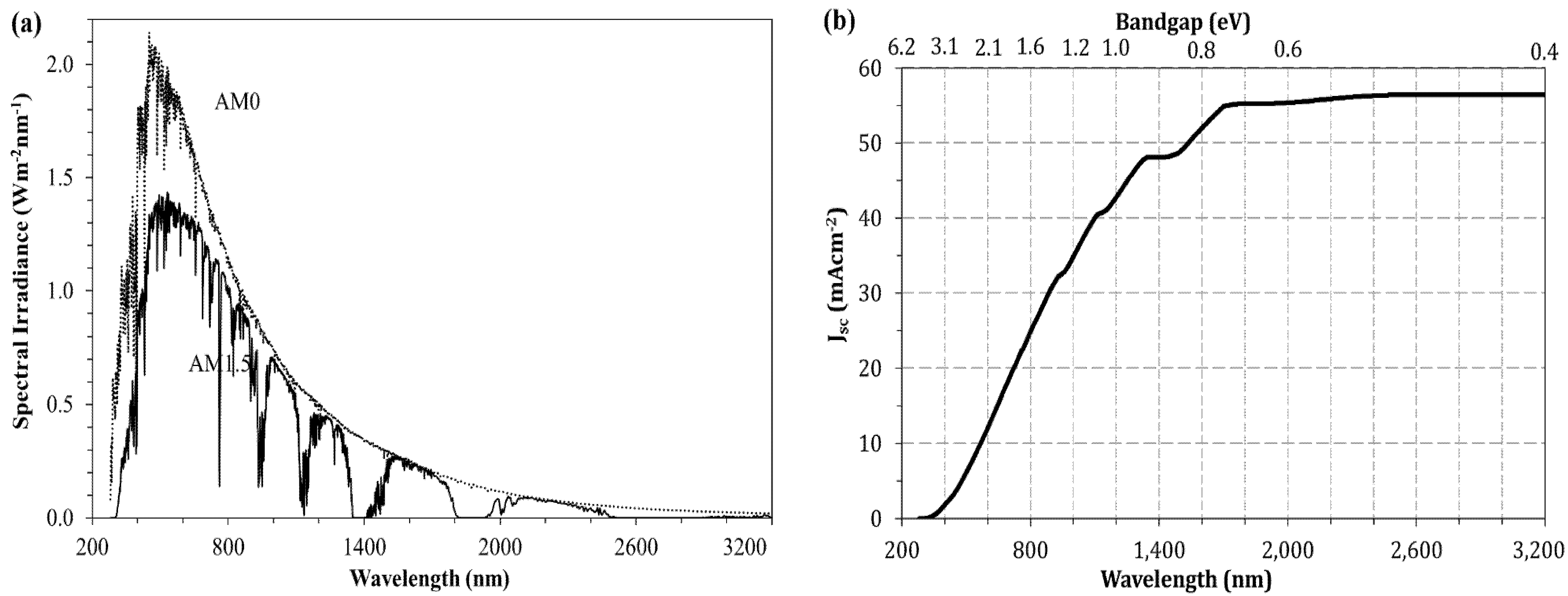
Figure 1a shows the AM0.0 and AM1.5 solar spectra as received above the air atmosphere and on the Earth’s surface, respectively. As a starting point, a theoretical calculation can be made to estimate J
sc as a function of wavelength (λ) or the corresponding energy gap (E
g) of the semiconductor. Assuming each photon creates one e-h pair, and there are no losses, J
sc can be calculated using data available in the literature [
8].
Figure 1b shows the results of such calculations and provides the maximum possible J
sc values obtainable by absorbing all photons in the solar spectrum. Making use of this graph, maximum possible J
sc values for different solar cells made with single bandgap materials can be estimated. These values are shown in
Table 1 for some solar cells currently under research and development.
Figure 1.
(a) The solar spectrum above the earth atmosphere (AM0.0) and at the Earth’s surface (AM1.5) and (b) the maximum short-circuit current density (Jsc) achievable when all photons are utilised to create one e-h pair each without any losses, as a function of wavelength or energy bandgap in eV.
Table 1.
Maximum possible J
sc from ideal homo-junctions based on different semiconductors when there are no losses within the device. These maximum J
sc values are obtained from the theoretically calculated graph shown in
Figure 1b.
Table 1.
Maximum possible Jsc from ideal homo-junctions based on different semiconductors when there are no losses within the device. These maximum Jsc values are obtained from the theoretically calculated graph shown in Figure 1b.
| Semiconductor Used in a Homo-Junction | Bandgap of the Semiconductor (eV) | Corresponding Wavelength (nm) | Maximum Possible Jsc (mA·cm−2) |
|---|
| CdTe (direct bandgap) | 1.45 | 855 | 27 |
| GaAs (direct bandgap) | 1.43 | 867 | 29 |
| Si (in-direct bandgap) | 1.10 | 1127 | 41 |
| InN, GaSb (direct bandgap) | 0.72 | 1720 | 55 |
| Ge | 0.67 | 1850 | 56 |
| PbS, InAs | 0.36 | 3440 | 57 |
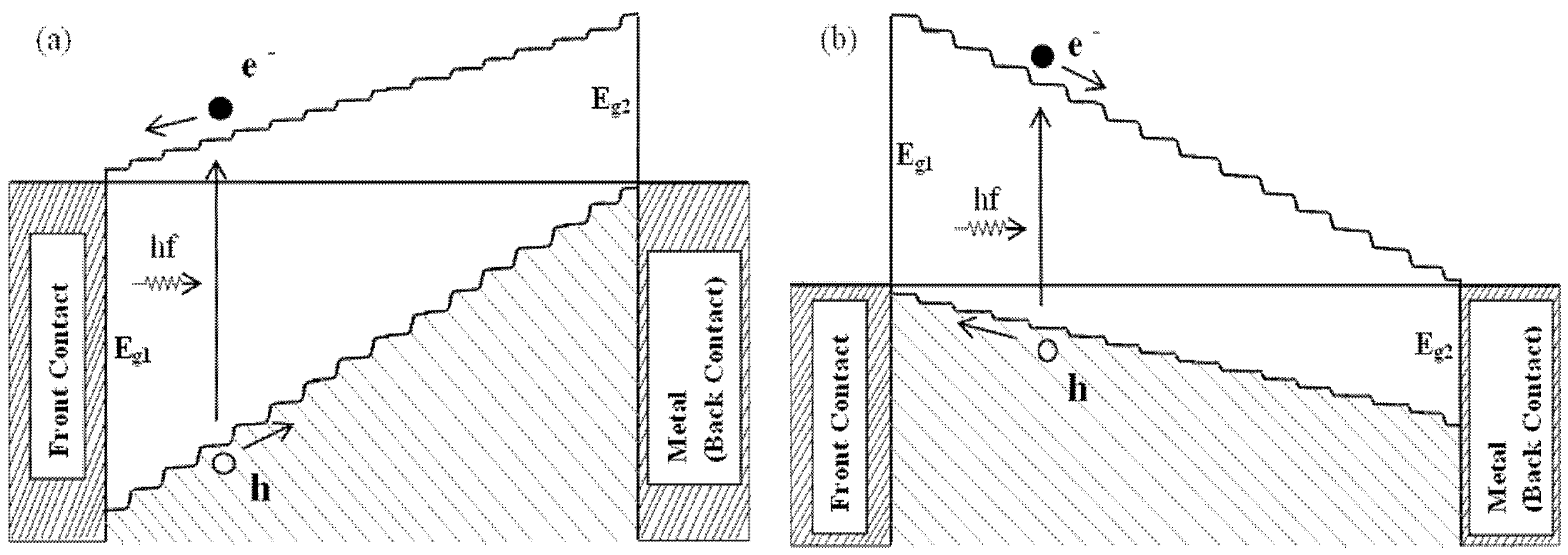
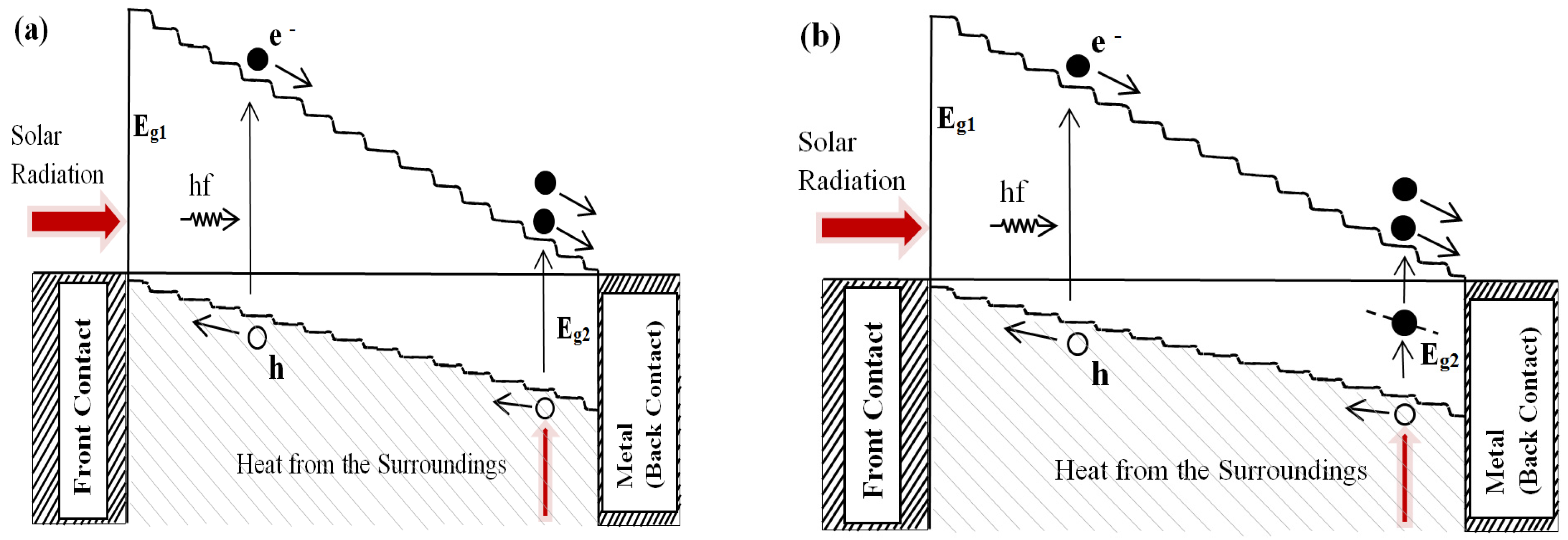
The challenge faced is how to harvest all photons available in the solar spectrum using one device. The most attractive method for solving this problem is by using a graded bandgap structure and combining both impurity PV effect and impact ionisation within one device.
To harvest all photons available in the solar spectrum, graded bandgap device structures as shown in
Figure 2 can be used [
1]. These devices can start with either an n-type or a p-type window material in the front. Out of the two structures, the device starting from the p-type window material is more attractive since the potential barrier height achievable for electron transport is larger than that of a device made on an n-type window material. By increasing E
g1, the slope of the bands or the built-in electric field can be increased. However, in both cases, the V
oc achievable depends on the smaller bandgap (E
g2). Therefore, E
g2 should be fixed at a value close to 1.40 eV in order to achieve high V
oc values above 1.00 V.
Figure 2.
Energy band diagrams of graded bandgap devices based on (a) n-type window material and (b) p-type window material. Note that the potential barriers achievable for electron transport is higher in devices based on p-type window materials.
Figure 2.
Energy band diagrams of graded bandgap devices based on (a) n-type window material and (b) p-type window material. Note that the potential barriers achievable for electron transport is higher in devices based on p-type window materials.
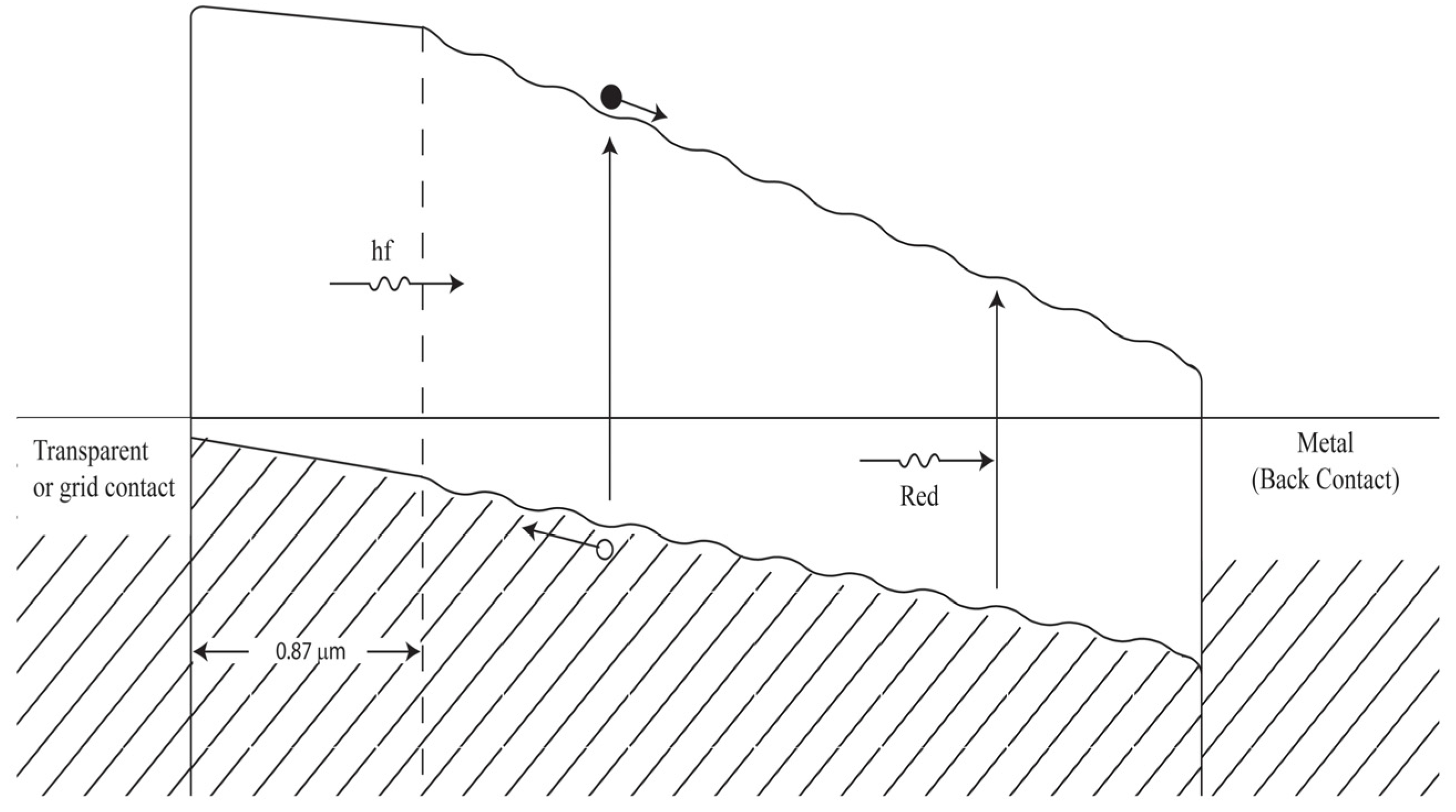
Such a device can absorb all photons available within the UV, visible down to energy value Eg2, but cannot absorb photons with energy less than Eg2. In order to absorb the IR radiation, impurity PV effect can be used in the same device structure utilising naturally occurring defect levels within the material.
2.2. Impurity PV Effect
In solar energy materials, there are so many different defects. The number of defects can be minimised by optimizing growth conditions and processing steps, but cannot be completely removed. These defects are usually detrimental during PV action, by drastically reducing photo-generated charge carriers through recombination process. The most sensible way forward is therefore to make use of these defects to work towards the enhancement of the device performance. This can be effectively done through proper design of the device structure. As shown in
Figure 3, in a graded bandgap device, the defects are available in the presence of a strong built-in electric field. In this situation, an IR photon can promote an electron from the valence band to defect level-1 (d1). Since the hole in the valence band is swiftly removed to the front contact, the electron in d1 level cannot relax back to recombine with the hole. Therefore, it remains there until another IR photon promotes it to level-2 (d2). This process continues until the electron is promoted to the conduction band and taken away to the back electrical contact. This is indeed the impurity PV effect, or the creation of e-h pairs using multi-step photon absorption process. Using this method, electrons can be pumped up-wards using all IR radiation available in the solar spectrum. This way, the graded bandgap solar cells can be used to harvest all photons in the UV, visible, and IR regions.
This also has an added advantage of absorbing the IR radiation available in the surroundings. The device, therefore, can be PV active in complete darkness [
9] and these experimental results are presented in
Section 4.3.
Figure 3.
Effective use of naturally occurring defects in semiconductors to create e-h pairs by multi-step photon absorption. Photons with energy less than the smallest bandgap (Eg2) can be harvested using the impurity PV effect.
Figure 3.
Effective use of naturally occurring defects in semiconductors to create e-h pairs by multi-step photon absorption. Photons with energy less than the smallest bandgap (Eg2) can be harvested using the impurity PV effect.
2.3. Impact Ionisation
Impact ionisation can also be effectively incorporated into this device due to its strong built-in electric field and the gradual decrease in the bandgaps across the device. Blue end photons with high energy create e-h pairs in the front of the device and minimise thermalisation. These electrons can accelerate across the device gaining high kinetic energy and may break another bond close to the rear of the device. This is an example of band-to-band promotion of electrons due to impact ionisation, as shown in
Figure 4a. This effect is also more prominent in structures based on p-type window materials, since the electrons are accelerated towards low bandgap semiconductors.
Figure 4.
Schematic representation of two types of impact ionisation (a) Band-to-band impact ionisation due to energetic electrons and the low bandgap materials towards the back of the device and (b) impact ionisation due to combination of photo-generated electrons and impurity PV effect utilising IR radiation from the solar spectrum and the surroundings.
Furthermore, e-h pairs can also be created by the combination of impurity PV effect and collisions between photo-generated electrons, and electrons promoted to defect levels. In this case, combination of an IR photon from the surroundings and a photon from the solar spectrum create two e-h pairs (see
Figure 4b). This has the highest probability of creating more e-h pairs in this device. In this case, the solar cell has two inputs; the solar radiation and the IR radiation from the surroundings. The support of IR radiation from surroundings helps one photon from the solar spectrum to create two e-h pairs. In this type of graded bandgap devices, J
sc can be increased to very high values due to following reasons.
(i) Ability to harvest all photons from UV, visible, and near IR regions of the solar spectrum due to grading of the energy bandgap.
(ii) Ability to use IR radiation available both in the solar spectrum and the surroundings, making use of built-in impurity PV effect.
(iii) Ability to have band-to-band impact ionisations and defect level-to-conduction band impact ionisations, by making use of IR radiation from the surroundings.
(iv) Ability to harvest photons simultaneously from surroundings in addition to the photons from the solar spectrum.
(v) Reduction of detrimental recombination process via defects, due to helpful impurity PV effect contributing to produce more photo-generated charge carriers within the device.
Therefore with optimised device fabrication of graded bandgap structures, extremely high Jsc values can be anticipated, showing over 100% quantum efficiency (QE) values.
3. Experimental Testing
The concept and the design given in
Section 2 are purely based on solid state physics and quantum mechanical principles [
1]. However, these ideas must be experimentally tested in order to prove its viability. In order to test these new ideas, it was empirical to use well understood semiconducting materials. AlGaAs alloy is the second most researched material next to silicon and therefore, this alloy was selected to experimentally test this new design.
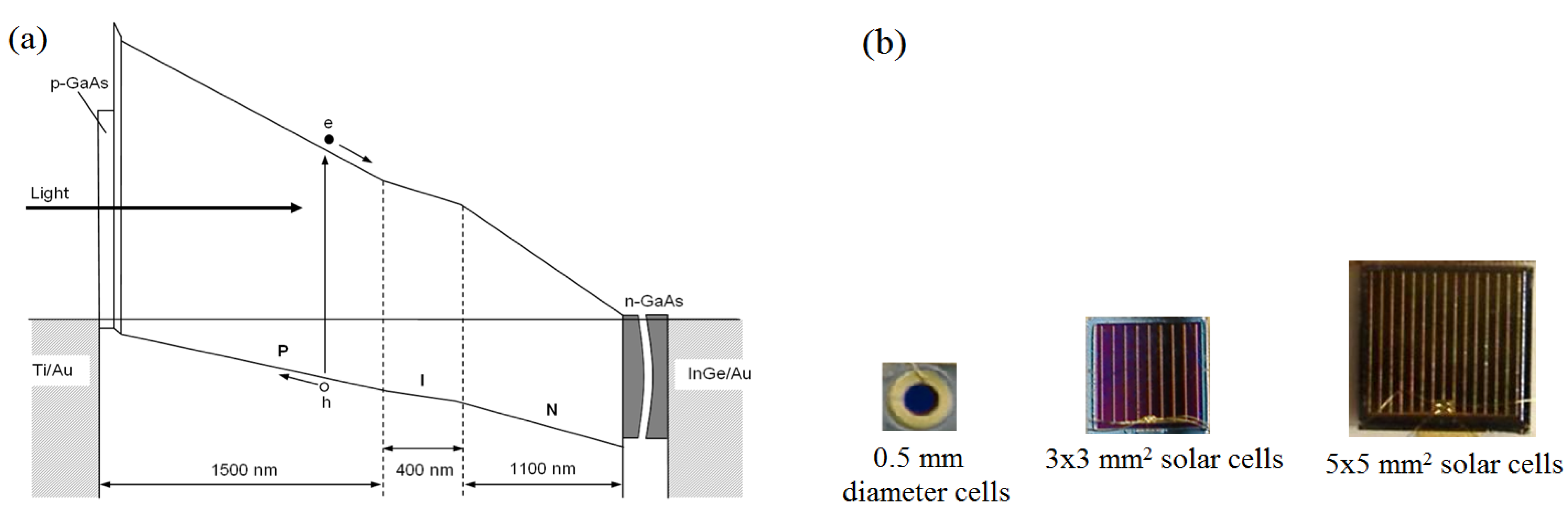
As shown in
Figure 5a, the growth of the device structure started from n-type GaAs (E
g~1.43 eV) wafer [
10,
11,
12,
13,
14]. Using MOCVD method, a thin layer of GaAs was grown on the wafer, and the aluminium (Al) content was gradually increased in order to increase the bandgap of the material. The alloy layer was grown up to 3 μm thickness, and the Al content was controlled to increase the bandgap from 1.43 eV to ~2.20 eV. In addition, the GaAs at the back of the device was doped n-type with Si. The Si concentration was gradually reduced towards the middle of the structure. Then, the p-type doping by C was gradually increased towards the front of the device. This way, the doping profiles were changed, to vary the doping of semiconductors from n- to p- from the rear to the front of the device. In the middle of the device, the material shows intrinsic properties.
After completion of the growth, a p-GaAs capping layer was used to prevent oxidation of Al incorporated in the film. During device processing, this layer was completely removed and grid type ohmic contacts were made on the p-type material in the front. Ohmic contacts were also fabricated on the n-type GaAs wafer at the back of the device. In this processing, an anti-reflection coating was also added to the front of this device. A picture of completed devices is shown in
Figure 5b. The device sizes were changed to produce 0.5 mm diameter, 3 × 3, 5 × 5 and 10 × 10 mm
2 sizes to check the effect of scaling up process. Completed devices were tested using current-voltage measurements in order to determine the device characteristics and solar cell parameters including the final conversion efficiency.
Figure 5.
(a) The schematic diagram of the graded bandgap device structure and (b) pictures of fully fabricated graded bandgap devices with different sizes.
Figure 5.
(a) The schematic diagram of the graded bandgap device structure and (b) pictures of fully fabricated graded bandgap devices with different sizes.
4. Experimental Results
4.1. Device Assessment Using Current-Voltage Characteristics
The current-voltage (I-V) characteristics were measured under dark conditions for small area (0.5 mm diameter) devices. The diodes showed good rectification properties exceeding rectification factors of 105 at 1.0 V. The ideality factors of these devices varied in the range 1.41–2.26, and the potential barrier estimated from low ideality factor devices was >1.38 eV.
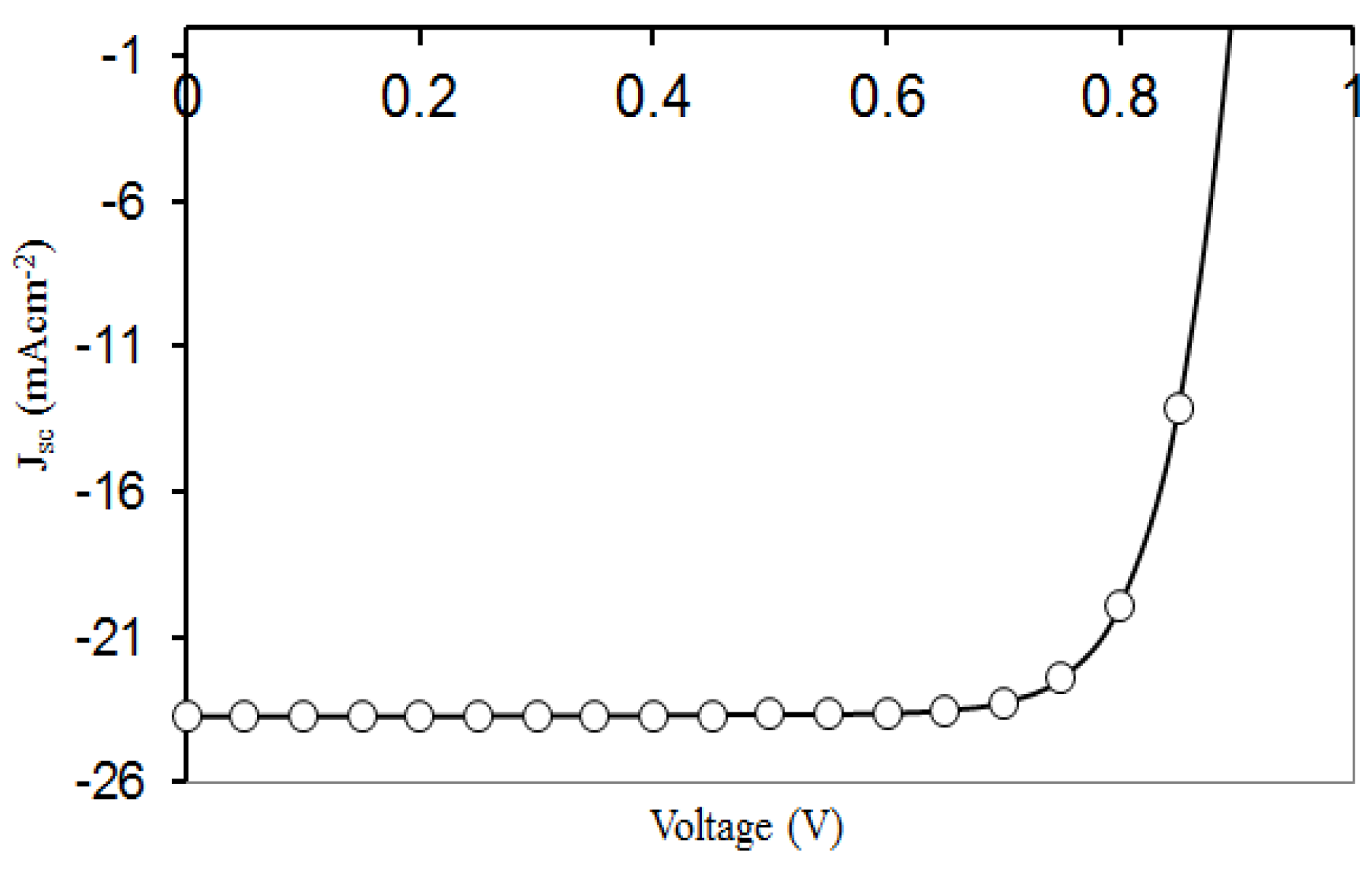
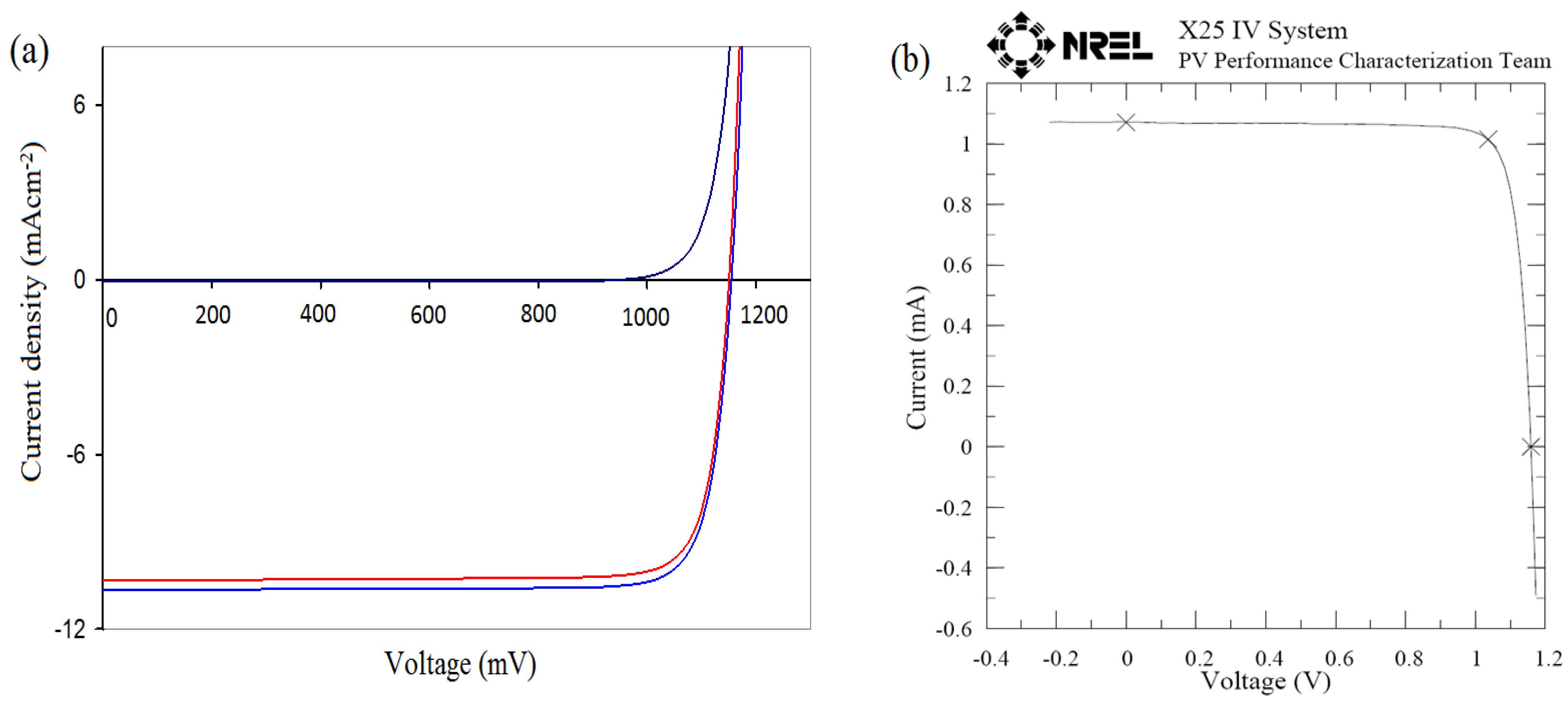
The I-V characteristics under AM1.5 conditions were measured for large area devices and typical results are shown in
Figure 6a,b. In order to check the accuracy, different devices from the same batch were measured in six different solar energy laboratories. The detailed cell parameters measured are summarised in
Table 2 for comparison.
Figure 6.
Experimentally observed I-V characteristics for graded bandgap devices fabricated using AlGaAs material.
Figure 6.
Experimentally observed I-V characteristics for graded bandgap devices fabricated using AlGaAs material.
Table 2.
The summary of solar cell parameters as measured in five different laboratories for comparison.
Table 2.
The summary of solar cell parameters as measured in five different laboratories for comparison.
| Device | Voc (mV) | FF | Jsc (mA·cm−2) | Place of Assessment |
|---|
| 1 | 1175 | 0.87 | 11.2 | SHU Labs, UK (Imyhamy M. Dharmadasa et al.) |
| 2 | 1160 | 0.86 | 12.1 |
| 3 | 1148 | 0.86 | 10.7 | Zürich Labs, Switzerland (Ayodhya Tiwari et al.) |
| 4 | 1141 | 0.86 | 10.3 |
| 5 | 1169 | 0.85 | 11.5 | SBU Labs, UK (Hari Reehal et al.) |
| 6 | 1149 | 0.86 | 10.0 |
| 7 | 1150 | 0.85 | 12.1 | EPFL Labs, Switzerland (Michael Grätzel et al.) |
| 8 | 1159 | 0.85 | 12.3 | NREL—USA (Tim Gessert et al.) |
| 9 | 1156 | 0.85 | 11.9 |
The highest Voc observed (1175 mV) for these devices are the highest reported for a single device to date. The FF values are well above 80% (0.85–0.87), and these are the highest achievable for a PV solar cell. It is interesting to note the observation of two highest parameters (Voc and FF) for the first growth as shown below, with low Jsc ~12 mA·cm−2 values. The device parameters did not vary with the size of the cells, as expected from epitaxial semiconducting layers. All devices fabricated were similar showing 100% yield and uniformity of the materials and devices.
Voc = (1141–1175) mV
FF = (0.85–0.87)
Jsc = (10.0–12.3) mA·cm−2
Efficiency ~ 12%
The GaAs based solar cells are capable of delivering much higher Jsc values than experimentally measured above values. These devices from the first growth have produced only ~12 mA·cm−2. This must be due to some severe losses within the devices fabricated from the first growth, and the QE measurements were carried out to find more about these losses.
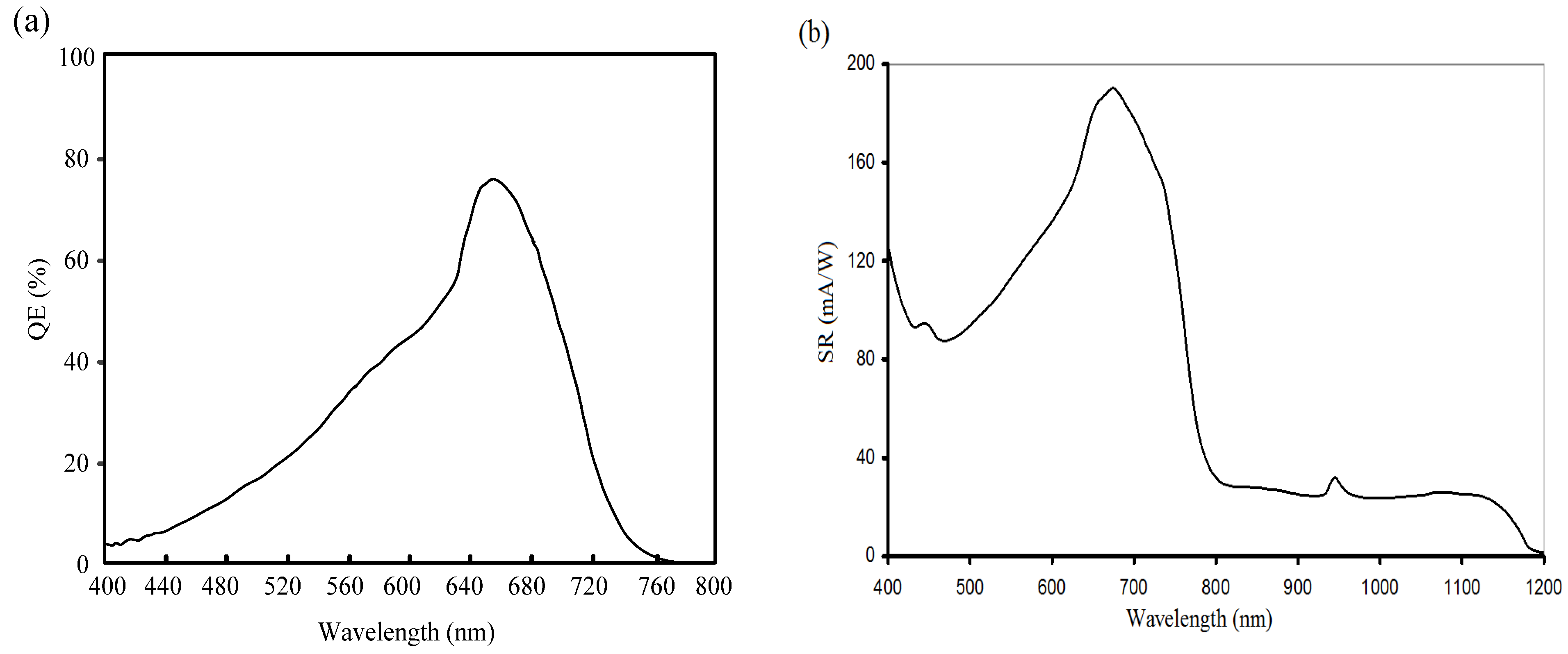
4.2. Quantum Efficiency and Responsivity Measurements
Quantum efficiency and responsivity measurements were carried out in several laboratories to identify these losses, and typical results are shown in
Figure 7.
It is evident from both QE and responsivity measurements that the losses are at both ends, causing low current density. In addition, the responsivity measurements indicate the collection from IR region, hinting the presence of impurity PV activity within this device. At the same time this indicates an inherent loss of data from QE measurements. This could arise during data acquisition, analysis or plotting procedure in current QE measurement systems.
Figure 7.
(a) A typical QE spectrum and (b) a Responsivity curve measured for graded bandgap solar cells. Note the severe loss in both blue and red ends of the spectrum. The IR collection in the responsivity curve is clear, but the QE measurements fail to detect the collection in this region.
Figure 7.
(a) A typical QE spectrum and (b) a Responsivity curve measured for graded bandgap solar cells. Note the severe loss in both blue and red ends of the spectrum. The IR collection in the responsivity curve is clear, but the QE measurements fail to detect the collection in this region.
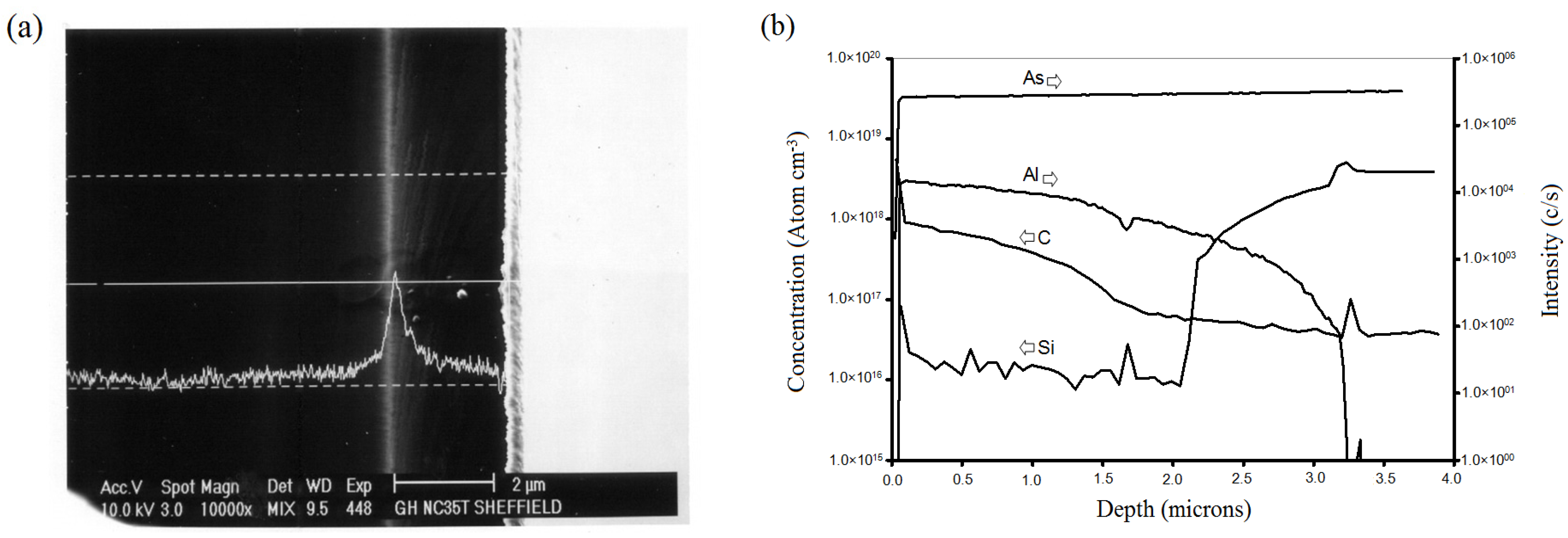
Further experimentation using electron beam induced current (EBIC) and secondary ion mass spectroscopy (SIMS) profiling gave clear information [
15] for severe losses at both blue and red ends (see
Figure 8a,b). Carbon p-doping in the front, and Si n-doping at the back were in 10
18–10
19 cm
−3 region creating flat-band conditions in the device. Therefore, the band diagram of the experimentally grown device is as shown in
Figure 9, instead of the anticipated device as shown in
Figure 3. Clearly, the e-h pairs created at the front and at the rear of the device were lost due to lack of built-in electric field for charge carrier separation and collection.
Figure 8.
EBIC and SIMS profiles of graded bandgap solar cell structures showing n+ and p+ doping at the back and the front of the solar cell.
Figure 8.
EBIC and SIMS profiles of graded bandgap solar cell structures showing n+ and p+ doping at the back and the front of the solar cell.
Figure 9.
The shape of the energy band diagram of the devices fabricated during first growth due to high doping concentrations at both ends of the structure.
Figure 9.
The shape of the energy band diagram of the devices fabricated during first growth due to high doping concentrations at both ends of the structure.
The obvious next step is to reduce the C and Si doping at the front and the back of the device to ~10
15 cm
−3 level [
16] in order to extend the depletion region to meet the two electrical contacts. However, this is only possible for Si doping with MOCVD method. C doping in the front cannot be reduced to ~10
15 cm
−3 using MOCVD since the reactor has background C during growth. The second growth was therefore carried out only by reducing the Si doping to improve the device. Typical experimentally measured I-V curve (see
Figure 10) and the device parameters observed are shown below.
Figure 10.
A typical I-V curve measured for the devices fabricated from the second growth after adjusting Si doping to ~1015 cm−3.
Figure 10.
A typical I-V curve measured for the devices fabricated from the second growth after adjusting Si doping to ~1015 cm−3.
Voc = ~900 mV
Jsc = (22–26) mA·cm−2
FF = (0.82–0.87)
Efficiency ~ 18%–20%
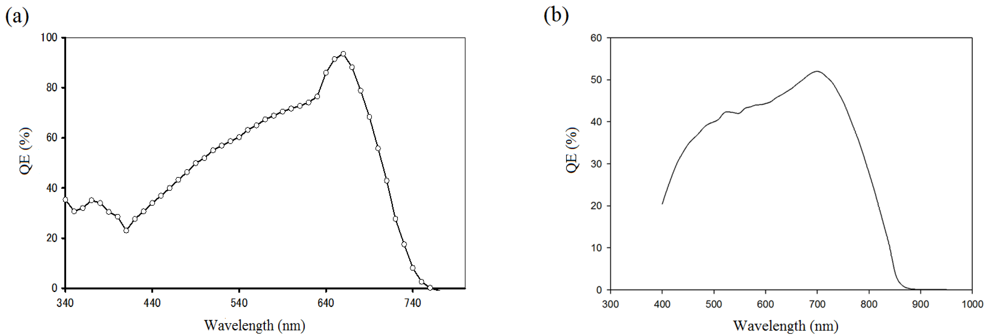
The QE measurements for the devices from the first and second growth are shown in
Figure 11 for comparison. The energy band diagram of the devices fabricated from the second growth (b) shows improvements, mainly in the red end. The reduction of silicon doping at rear of the device has considerably improved the collection in the red end by shifting the cut-off wavelength from ~740 nm to ~870 nm. This process has clearly improved the creation and collection of charge carriers from the red-end. Therefore, the J
sc value has doubled to ~24 mA·cm
−2. An improved band diagram, based on the reduced Si doping concentration is shown in
Figure 12. The efficiency of the devices from the second growth increased to ~18%–20%.
Figure 11.
Typical QE curves measured for devices fabricated from the first growth (a) and the second growth (b). The losses in both blue and red ends are evident for the first set of devices, but the collection at the rear has improved showing the red-end cut-off moving from ~740 nm to ~870 nm.
Figure 11.
Typical QE curves measured for devices fabricated from the first growth (a) and the second growth (b). The losses in both blue and red ends are evident for the first set of devices, but the collection at the rear has improved showing the red-end cut-off moving from ~740 nm to ~870 nm.
Figure 12.
Shape of the energy band diagram of the improved devices with lower Si doping at the back of the solar cell.
Figure 12.
Shape of the energy band diagram of the improved devices with lower Si doping at the back of the solar cell.
It should be noted that the change in V
oc from ~1170 mV to ~990 mV for the second growth was due to the difference in the orientation of the two GaAs wafers used, and therefore the potential barrier heights available in the two devices have changed. Although this is not a good news for the devices, it shows experimental evidence for the Fermi level pinning effects are also common for GaAs based devices as clearly observed for CdTe [
17] and CIGS [
18] devices.
The next stage is to reduce the C doping in the front of the device to ~10
15 cm
−3 [
16], in order to extend the depletion region to the front electrical contact and produce an expected improved results from this device. MOCVD technique cannot reduce the C doping since C is present in the reactor. This can only be done using a growth method such as molecular beam epitaxy (MBE). Once both doping issues are achieved, some excellent results are anticipated from this device structure. This needs a competent MBE grower's attention to achieve devices with some extra-ordinarily high device parameters. This is also an excellent device to test with nitride compounds to achieve high performing solar cells.
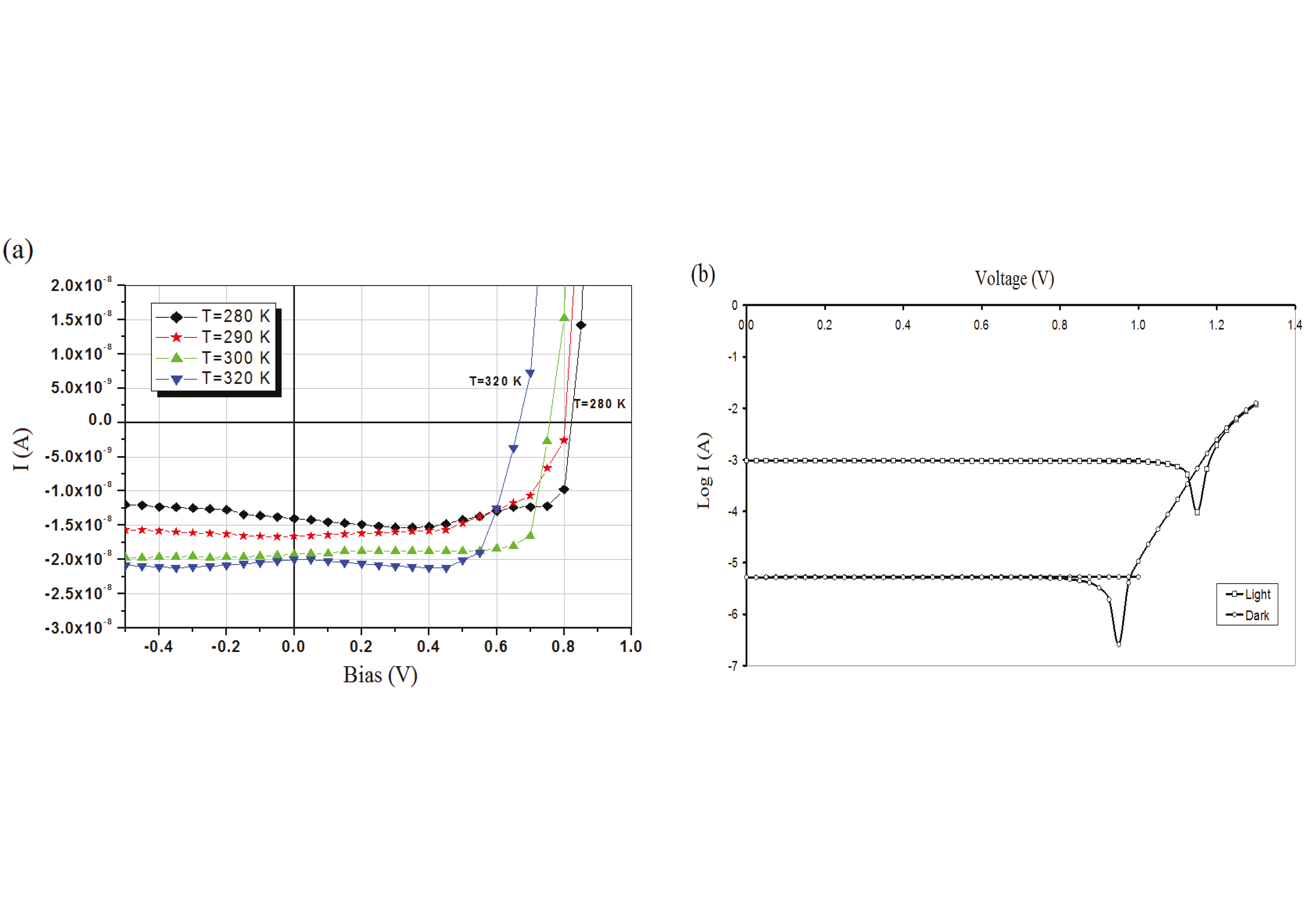
4.3. Experimental Evidence for Impurity PV Effect
At the design stage, impurity PV effect was incorporated and expected in the graded bandgap device structure. The presence of this effect was first hinted by the responsivity measurements, as shown in
Figure 7b. In order to experimentally test this effect further, these devices were measured in complete dark conditions removing the input from direct solar radiation.
Figure 13a shows the linear-linear I-V curves of these devices when measured in a cryostat which completely removes the direct solar radiation. The I-V curves were measured as a function of temperature in order to investigate their behaviour. At room temperature, this particular device produces ~700 mV, as V
oc and the behaviour of both V
oc and J
sc with temperature is as expected from a normal PV device.
Figure 13.
(a) Linear-linear I-V curves at different temperatures under complete darkness and (b) log (I)-V curves measured under dark and AM1.5 illuminated conditions. Note the production of Voc values above ~950 mV in complete dark conditions indicates the presence of impurity PV effect.
Figure 13.
(a) Linear-linear I-V curves at different temperatures under complete darkness and (b) log (I)-V curves measured under dark and AM1.5 illuminated conditions. Note the production of Voc values above ~950 mV in complete dark conditions indicates the presence of impurity PV effect.
Figure 13b shows the log(I)-V curves for similar device, measured using a different I-V measurement system. The kink in the log(I)-V curve indicates the V
oc of the solar cell. This device produces ~1175 mV under AM1.5 illumination, while a V
oc of 950 mV is produced under complete darkness [
9].
Measurements of I-V curves under complete darkness and the responsivity measurements provide experimental evidence for the presence of impurity PV effect as expected in the design stage. When the devices are kept in complete darkness, IR radiations from the surroundings create e-h pairs using multi-step photon absorptions as presented in
Figure 3. This process is active mainly due to the existence of a strong electric field in the device due to the graded bandgap nature of this structure. When the defects are involved in up-pumping of electrons using IR radiation, the probability of recombination process (down-pumping of electrons) is reduced, helping to increase the short circuit current density.
The above effect is experimentally observed when the diode ideality factor (
n) was measured under dark and illuminated conditions.
Table 3 shows the
n-values observed from the forward portion of I-V curves. It is evident that the
n values observed under illumination are much lower than those observed under dark conditions. Clearly, the recombination process is reduced under illumination. This could happen due to saturation of defects in the presence of photo-generated charge carriers, and the involvement of defects in electron up-ward pumping process, or due to the combination of both.
Table 3.
The ideality factors for AlGaAs based graded bandgap solar cells under dark and illuminated conditions showing reduced recombination contributions under illumination.
Table 3.
The ideality factors for AlGaAs based graded bandgap solar cells under dark and illuminated conditions showing reduced recombination contributions under illumination.
| Solar Cell Number | 1 | 2 | 3 | 4 | 5 |
|---|
| n value under dark conditions | 1.41 | 1.50 | 1.68 | 1.84 | 2.26 |
| n value under illumination | 1.13 | 1.15 | 1.22 | 1.14 | 1.91 |
4.4. Experimental Evidence for Impact Ionisation Effect
Because of the correct material selection and the bandgap engineering of the design of this device, two types of impact ionisations are possible, as shown in
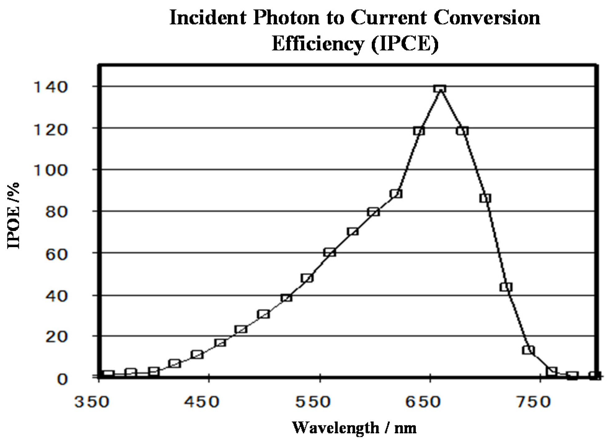
Figure 4. This was also experimentally tested using incident photons to current conversion efficiency (IPCE) measurements.
Figure 14 shows an IPCE measurement results obtained for one of these devices. It shows 140% IPCE value, clearly demonstrating the presence of impact ionisation in these solar cells. Although the device is not fully optimised, the 140% IPCE value indicates the production of more than one e-h pair per photon in these devices. Once fully optimised, the effect of this contribution will be evident by an enhancement in the J
sc values.
These experimentally observed positive results demonstrate how naturally occurring defects in semiconductors can be used to enhance solar cell parameters. As shown in this work, the defects present in semiconducting materials can be used to positively contribute to PV effect via impurity PV effect and impact ionisation. However, it should be noted that intentional addition of mid-gap states can be detrimental in practical devices due to introduction of drastic recombination and generation process. Therefore, in order to make high performance devices, the materials should be grown with minimum possible defects, and these residual defects should be used to positively contribute to PV action by properly designing the bandgap variation within the device.
Figure 14.
IPCE curve measured for a graded bandgap solar cell structure. Note the 140% IPCE value around 650 nm, even with severe losses at both blue- and red-ends of the spectrum.
Figure 14.
IPCE curve measured for a graded bandgap solar cell structure. Note the 140% IPCE value around 650 nm, even with severe losses at both blue- and red-ends of the spectrum.
5. Graded Bandgap Devices Utilising Rod-Type Materials
All the advantages of graded bandgap devices described in the above sections can be combined with the advantages of devices fabricated utilising nano- and micro-rod-type materials. A schematic diagram of an ideal solar cell that can be fabricated with rod-type materials is shown in
Figure 16. As an example, CdS/CdTe thin film solar cell has been taken to illustrate this development. This solar cell has the basic structure of glass/FTO/CdS/CdTe/metal, and the structure undergoes a CdCl
2 treatment followed by heating in air prior to surface cleaning and fabrication of back metal contact. According to the latest understanding of involved materials and processing [
19,
20], the following section describes the main features of this device and its PV function.
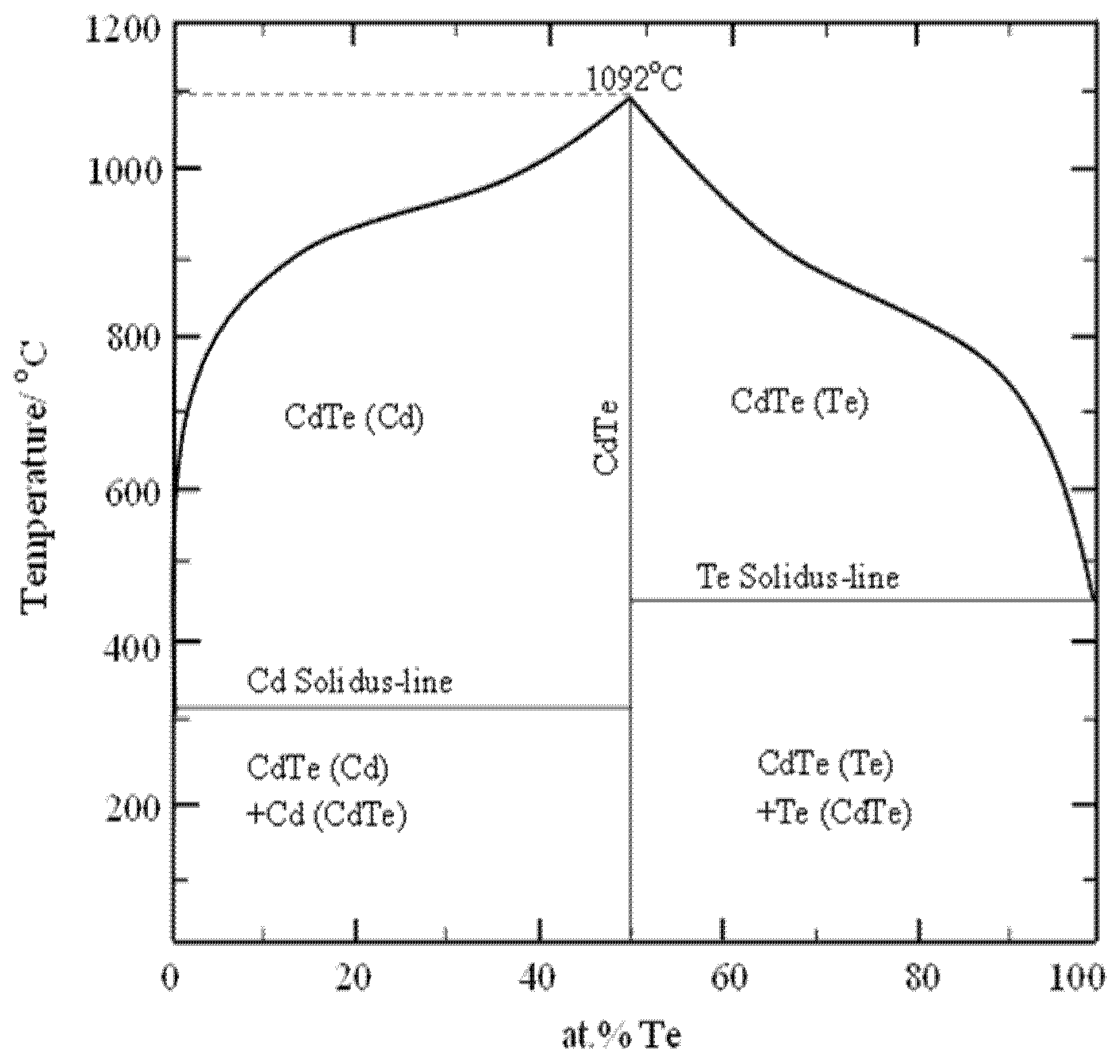
In order to understand the changes taking place during heat treatment in the presence of CdCl
2, the phase diagram of CdTe shown in
Figure 15 is extremely useful. According to the phase diagram, the melting point of stoichiometric CdTe is 1092 °C. The melting points of Cd-rich and Te-rich CdTe could reduce down to 322 °C and 450 °C, respectively, depending on the amount of excess elements present. It is also a well-established phenomenon that the melting point of any pure material is drastically reduced due to addition of impurities. In this respect, when the polycrystalline CdTe layers are heat treated in air, in the presence of CdCl
2, excess Cd, Cl, and O can be considered as impurities in CdTe. Since these impurities are mainly accumulated in grain boundaries and the top surface, the materials on the surface and along the grain boundaries melt during heat treatment, in the temperature range of ~300 °C to ~450 °C. Pure CdTe grains with melting point of 1092 °C remain as floating solids, but their original preferential orientations can suddenly change to a random orientation. This sudden change of (111) preferential orientation, has been observed by collapsing of (111) XRD peak intensity at a temperature of 385 °C ± 5 °C [
20,
21].
Figure 15.
Phase diagram showing the melting point of CdTe as a function of its composition. Re-drawn from [
22].
Figure 15.
Phase diagram showing the melting point of CdTe as a function of its composition. Re-drawn from [
22].
During heat treatment of the glass/FTO/CdS/CdTe structure in the presence of CdCl
2, a liquid layer is formed at the surface and grain boundaries, and Cl is readily mobile along the grain boundaries down to the CdS layer. Although the grain boundaries are melted at heat treatment temperatures ~(300 °C–450 °C) due to presence of elements like extra Cd, Cl and O, the columnar shaped CdTe grains remain as solids due to its high melting point of 1092 °C. Therefore the diffusion of Cl is slow into the body of crystalline grains in the layer [
23]. The Cl-diffused layer is simply a thin skin for each CdTe grain existing between the CdS and the free surface of the thin film. Cl diffusion tends to change the doping concentration of the skin around each CdTe grain [
23] (see
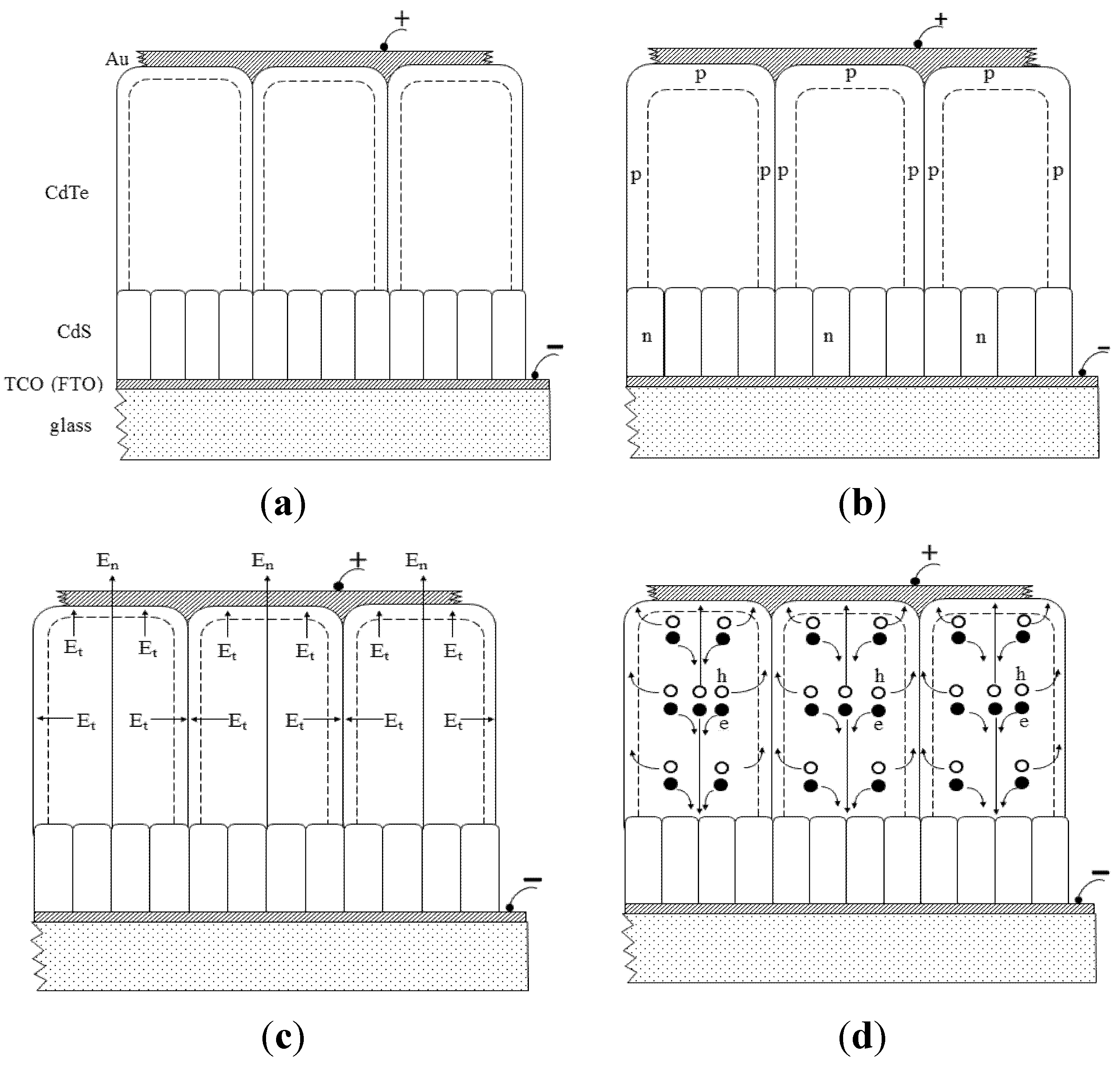
Figure 16b). As a result, a lateral electric field (E
t) is created in addition to the main electric field E
n (see
Figure 16c). The effect of these two fields is the flow of one carrier (say holes) along the grain boundaries to the back contact and flow of the other carrier (electrons) along the middle of the rod-type grains to the front contact. Since the number of photo-generated electrons and holes are equal in number and the grain boundary paths are narrow when compared to the cross section of the grains, the current density flowing along the grain boundaries are much higher than that along the grains. Therefore, the cross-section EBIC images should show brighter grain boundaries when compared to the body of the columnar shaped grains or pillars. This has been reported recently by other groups [
24,
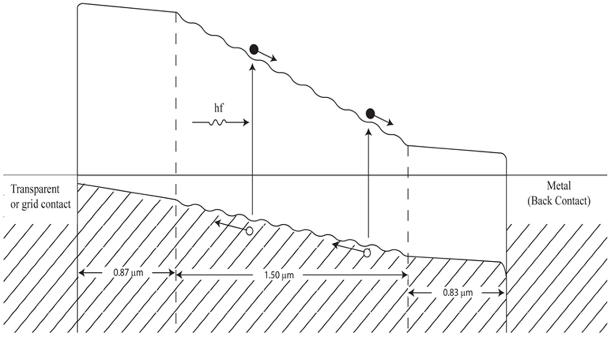
25] experimentally showing these effects. This unique charge carrier creation and separation within the material provides two separate paths for electrons and holes, and therefore minimises the recombination of charge carriers through annihilation. This is another advantage introduced by rod-type materials in solar cells. In fact, this special situation creates vertical junctions around grain boundaries in addition to the main horizontal junction formed at CdS/CdTe interface (for a p-n junction device) or at CdTe/metal interface (for an n-n hetero junction + Schottky barrier at the back contact device).
Figure 16.
Schematic diagram of (a) rod-type CdS/CdTe solar cells; (b) doping effects of grains after CdCl2 treatment; (c) presence of local electric fields (Et) in addition to the main electric field (En) within the device; and (d) photo-generated charge carrier creation, separation, and collection with high current densities along grain boundaries.
In addition to the drastic reduction of charge carrier annihilation, photo-generated charge carriers should have highest possible mobility values in rod-type CdS and CdTe. Rod-type materials grow with highest crystallinity and therefore photo-generated charge carriers flowing normal to the FTO substrate do not undergo many grain boundary scattering events.
If mobility is measured using Hall Effect, the mobility (µ‖) will be extremely low due to carriers crossing grain boundaries when transported parallel to the FTO substrate. Charge carriers undergo severe scattering due to millions of grain boundaries. It should also be noted that the Hall Effect measurements cannot be accurately performed on thin layers grown on FTO layers. This is mainly because of the current flow through the least resistive path, along the FTO layer. The solar cells made with rod-type materials or pillars normal to FTO should have high device parameters, due to reduced charge carrier annihilation and highest mobility of charge carriers across the device structure. The charge carrier mobility along fully crystallised pillar type materials (µ┴) can be several orders of magnitude larger due to minimum scattering during movement of charge carriers normal to FTO surface during PV action. Therefore, the use of Hall mobility (µ‖) to explain or theoretically model the PV activity of thin film solar cells is erroneous, when the layers consists of columnar type grains across the device. This explanation can also be valid for any thin film solar cells, such as CuInGaSe2 or perovskites, if the material layers consist of columnar type grains across the thickness.
One disadvantage created by the rod-type material is the easy formation of pin-holes, which short-circuit the device. However, the introduction of a pin-hole plugging layer can eliminate this disadvantage, keeping the above mentioned extra-ordinary advantages to increase device performance. Combining all the advantages of rod-type materials, it is possible to fabricate graded bandgap devices using electroplated materials.
Having designed the graded bandgap solar cells for developing next generation solar cells, and experimentally proving the concept utilising a well-researched AlGaAs material achieving excellent device parameters, our aim is to fabricate these types of devices using low-cost and scalable electrodeposited semiconductors. The preliminary work on glass/FTO/n-ZnS/n-CdS/n-CdTe/Au graded bandgap devices has shown over 10% efficiency with J
sc~48 mA·cm
−2. Full details of materials growth and processing steps will be published in a separate article [
2] in this Special Issue. These high current densities are positive signs of high potential of graded bandgap devices to develop next generation solar cells. In the conversion efficiency expression; η = V
oc × J
sc × FF/P
in, both V
oc and FF values are saturating at their possible achievable values. The efficiency can be doubled or tripled only by doubling or tripling the J
sc values by effective harvesting of photons available in the solar spectrum and in the surroundings. Reader’s attention is drawn to this initial but detailed experimental work presented in the next paper in this issue.
6. Conclusions
The work presented in this paper leads to several conclusions.
(i) A graded bandgap device has been theoretically designed to effectively harvest photons from UV, visible and IR regions, and to incorporate both impurity PV effect and impact ionisation in one single device.
(ii) This design has been experimentally tested using one of the most researched semiconducting, AlGaAs/GaAs layers. Excellent solar cell parameters have been observed (Voc ~ 1175 mV, FF ~ 0.86) within only two growths achieving ~20% conversion efficiency.
(iii) These fully fabricated devices are experimentally tested for the existence of impurity PV effect. Production of Voc > 700 mV in complete darkness and the responsivity signal in IR region confirm the contribution of impurity PV effect to the overall PV action of this device. The devices are also capable of harvesting IR radiation from the surroundings, through impurity PV effect.
(iv) As expected from the design, graded bandgap devices also contribute to current collection through impact ionisation. Experimental test shows 140% of IPCE signal confirming this contribution. In these devices, there are two components of impact ionisation; band-to-band impact ionisation and the combination of impurity PV effect and impact ionisation via native defect levels.
(v) The graded bandgap devices fabricated using MOCVD grown AlGaAs/GaAs requires the optimisation of the doping concentration especially in the front of the device. This can only be achieved by MBE growth method to produce higher efficiencies.
(vi) The devices based on nano- and micro-rod type materials have a great potential to fabricate graded bandgap devices, and achieve extra-ordinarily high device parameters in next-generation solar cells.
(vii) Experimentally measured charge carrier mobility using Hall Effect is not applicable to explain the PV activity of thin film solar cells made out of columnar type material grains. Photo-generated charge carriers travel across the layer along columns or rod type grains and therefore could have several orders of magnitude high mobilities. These are the extra-ordinary properties that can be expected from nano-materials based devices.


