Article

High Step-Up 3-Phase Rectifier with Fly-Back Cells and Switched Capacitors for Small-Scaled Wind Generation Systems

1
School of Electrical Engineering and Automation, Tianjin University, Tianjin 300072, China
2
State Grid Tianjin Electric Power Company, Tianjin 300072, China
3
State Grid Jiangxi Electric Power Company Repair Branch, Jiangxi 330000, China
*
Author to whom correspondence should be addressed.
These authors contributed equally to this work.
Energies 2015, 8(4), 2742-2768; https://doi.org/10.3390/en8042742
Submission received: 26 November 2014 / Revised: 7 March 2015 / Accepted: 1 April 2015 / Published: 10 April 2015
(This article belongs to the Collection Wind Turbines)

Abstract

:
This paper proposes and discusses a novel AC/DC converter suitable for small-scaled wind power generation system applications. By introducing flyback cells into the three-phase single-switch Boost circuit, the proposed converter is designed as single-stage and has both rectification and high step-up power conversion functions. It is able to obtain high voltage gain at low input voltage level, and high efficiency, low total harmonic distortion (THD) at rated power. The inherent power factor correction (PFC) is also determined, and can reach 0.99. Besides, since no electrolytic capacitor is employed and high voltage gain is achieved, the converter can also collect weak power at low input voltage in combination with energy storage devices, and contribute to a better low-wind-speed/low-power performance. Finally, a 400 W prototype is built to verify the theoretical analysis, and its efficiency is 87.6%, while THD is 7.4% at rated power.

1. Introduction

In face of the serious energy and environmental pollution crisis, lots of researchers have looked to renewable sources to find solutions. Wind power generation, as an indispensable part of the energy mix, has already shown its competitiveness and reliability to governments, electricity producers and customers all around the world. The rapid growth of the wind generation is surprising: 17.6 GW of wind capacity was installed in the first half of 2014, and the cumulative worldwide wind power capacity is expected to reach 360 GW by end of 2014. The prospects for wind power investment remain positive [1]. Wind generation systems (WGS) containing power electronics devices are often adopted to guarantee high quality electric power supply. Various power electronics converters applied for wind generation have been reviewed and compared in [2]. Most of them are applied for medium and large power levels and few focus their attention on low power level wind power generation, although small-scale wind power generation systems (e.g., under 1 kW) are commonly used on domestic roofs in power-hungry areas, including mountainous or insular regions. Thus, more research on distributed, small-scale wind application should be conducted. A considerable number of the existing small-scale WGS still simply copy the structures, designs and control methods for medium- and large-scale WGS, and are unable to meet the practical requirements of the smaller scale scenarios.
Compared to large-scale power level wind generation, small-scale WGS possesses advantages of higher flexibility for distributed applications, lower cost and reduced impact on the power grid, thus further research on this topic and its promotion are of great value.
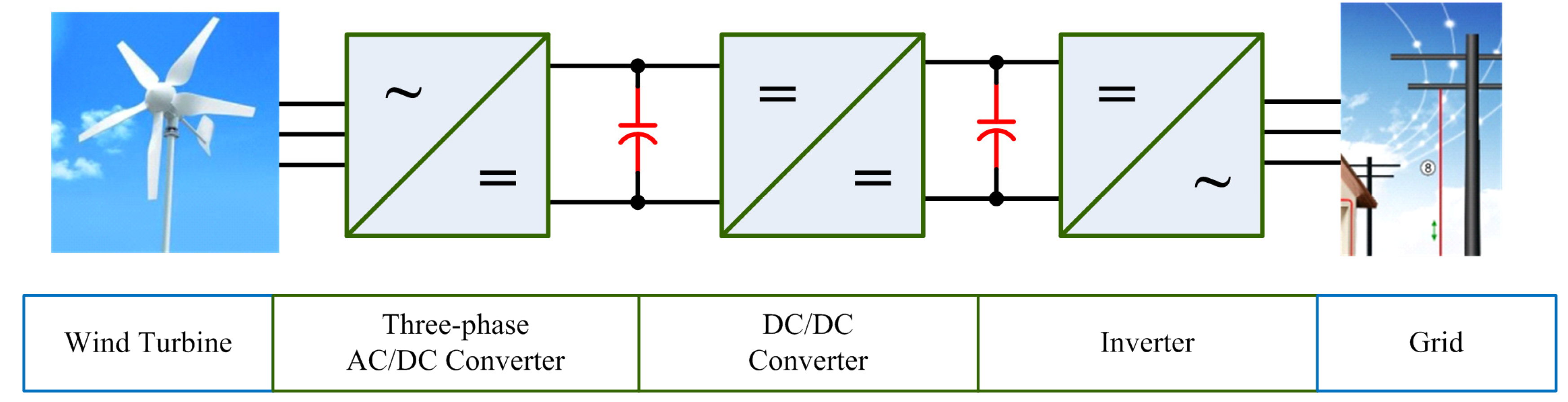
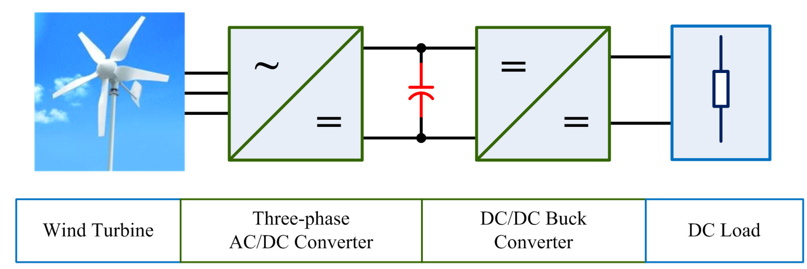
Usually, small-scaled WGS can be classified into two application forms: off-grid and grid-tied. Off-grid wind generation systems [3,4,5,6] are one available form for small-scale wind applications. An off-grid system usually includes a wind generator, a three-phase AC/DC rectifier, a DC/DC Buck converter and the load, as shown in Figure 1.
Figure 1. Block diagram of the off-grid wind generation system.
Energies 08 02742 g001
After rectification by the AC/DC circuit, the collected wind energy is further regulated by the Buck converter and delivered directly to the DC load. In [
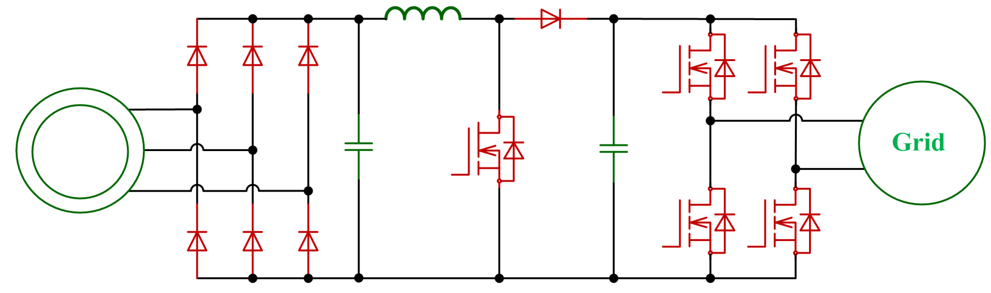
3], a converter for off-grid usage is proposed. By the combination of a three-phase diode bridge rectifier and an interleaved Buck converter, wind energy is converted to the load as power supply. The converter also realizes soft switching for the power switches, which can bring about higher conversion efficiency. Besides, for the general case, the load voltage level always remains low in off-grid WGS, therefore no particular requirements for the DC-link voltage level are needed. Instead, only a simple match for the voltage levels of wind generator, DC-link and the load is required. Thus, the off-grid WGS is relatively easy to realize. However, its applications are limited, because generally, off-grid systems are only suitable for special loads with a narrow voltage/power range. Conversely, as a more extensive application form, grid-tied WGS are often made up of a wind generator, a three-phase AC/DC rectifier, a DC/DC converter, an inverter and the grid, as shown in Figure 2.
Figure 2. Traditional structure of small-scaled grid-tie wind generation system.
Energies 08 02742 g002
Due to the changeable amplitude and frequency, the alternating electric power generated by the generally adopted permanent magnet synchronous machine (PMSM) must be converted into DC power form first, where the low-cost solution of the three-phase diode bridge rectifier is often used. Then, the DC power is further inverted to AC power again and delivered into the grid. The DC-link voltage should be designed to be higher than the grid voltage to fulfill grid-tie generation [2]. Unfortunately, in small-scale wind fields, the low average and large fluctuation of wind speed will result in rapid fluctuations and low output voltage of the wind generator. The output voltage provided by existing AC/DC converters using the maximum power point tracking (MPPT) control strategy is also very low and cannot match up with the required DC-link voltage level for the post-stage grid-tie inverter. Besides, the disability of the power converters to obtain adequate voltage gain at low input voltage, the disability of collecting weak wind energy, and the rigid requirements of the inverters for grid-tie generation also hinder its normal operation. Accordingly, for most existing small-scale WGS it is hard to realize a well-performed grid-tie wind power generation. Several topologies for small-scale WGS have been already researched and compared, as presented in [7,8,9,10,11,12,13,14,15,16,17,18,19,20,21,22,23]. A classical small-scale grid-tie WGS topology, consisting of diode bridge rectifier, DC/DC boost converter and grid-tie inverter is analyzed in [7,8,9] and shown in Figure 3. This topology possesses advantages like a simple structure, low cost and easy control. In [7], a converter consisting of wind turbine, PMSM generator, three-phase diode rectifier, boost DC/DC circuit, inverter and an LCL filter is analyzed, and can basically realize the wind power delivery. However, the promotion of this converter is limited. On the one hand, although the DC/DC boost circuit can provide a high voltage gain, it has drawbacks like high power losses and reduction in reliability. On the other hand, the three-phase diode bridge rectifier is a cost-efficient alternative for small-scaled wind generation, due to its low cost and simple configuration, but it still suffers from high power losses, caused by larger input current, and low power factor, which will introduce rich harmonics and may give rise to vibration, large noise and power resonance [10,11,12].
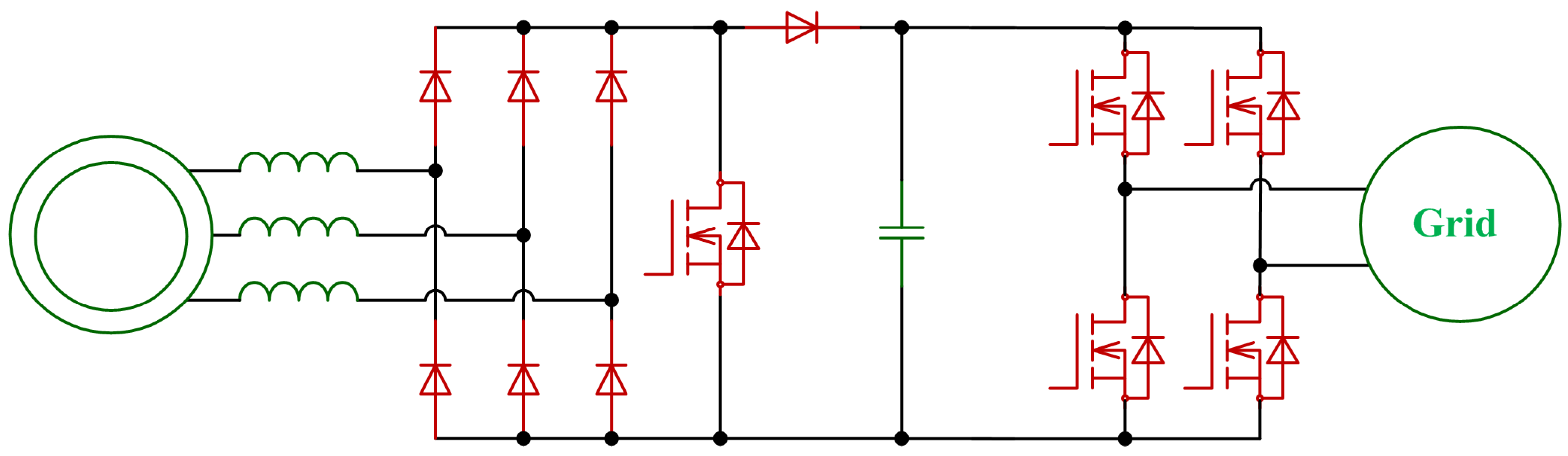
To overcome these problems, the back-to-back three-phase pulse width modulation (PWM) converter, as the most frequently used three-phase power converter topology so far in wind turbine systems, was developed [2]. In [13,14], the back-to-back PWM power conversion configuration is chosen and analyzed, as presented in Figure 4. The PWM converter substitutes the diode devices by full controlled switches in both generator side and grid side, and decouples the two sides by a bulky DC-link capacitor. It achieves bidirectional power delivery and has a wide power range of applications, from kW to MW by adopting different levels of power devices. The PWM converter can also obtain outstanding performances of high efficiency, unity power factor and high reliability, but in view of the complicated control strategy and higher cost, which is an important factor of the design purpose, the PWM converter is not the optimal alternative for small-scale WGS [15,16].
Figure 3. Diode bridge + boost converter wind generation system.
Energies 08 02742 g003
Figure 4. The PWM converter wind generation system.
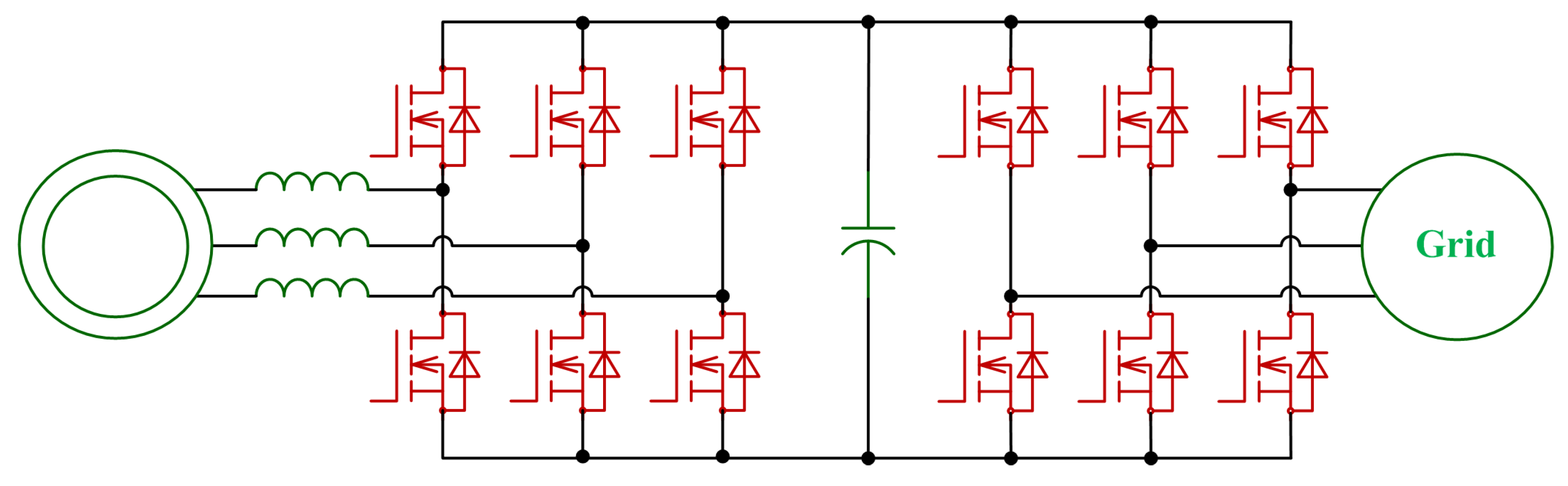
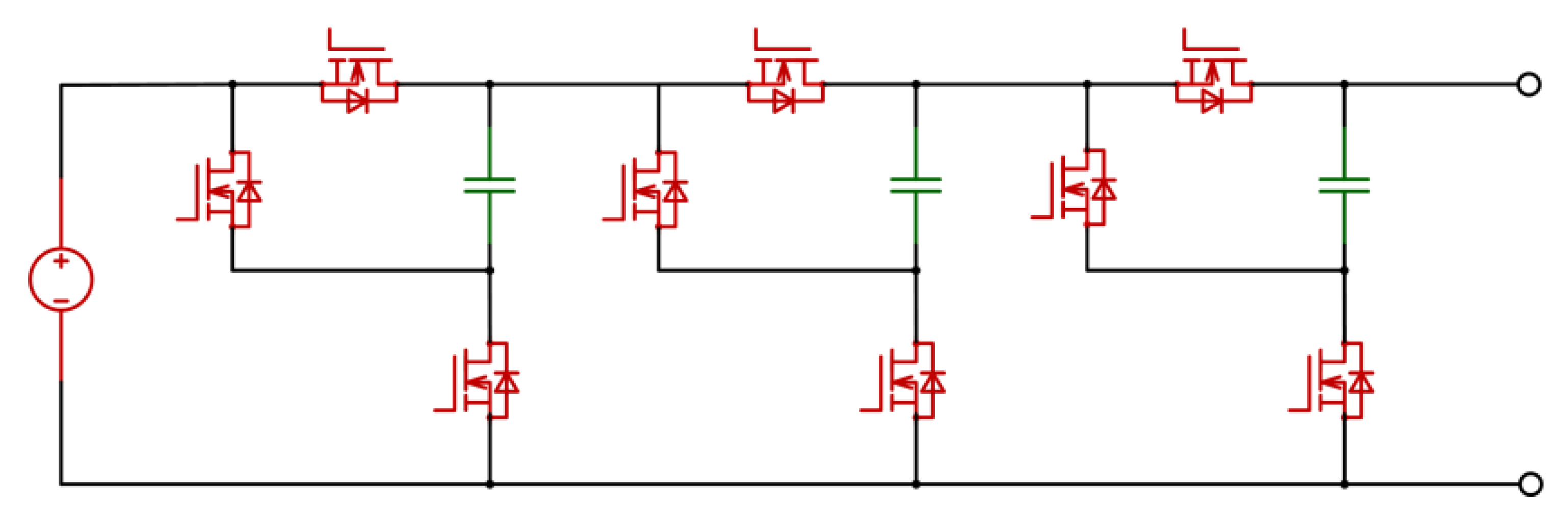
Energies 08 02742 g004
In [17,18], matrix converters are proposed and analyzed for small-scale WGS as shown in Figure 5. It is made up of full controlled switches with no passive components, and can adjust its current and voltage waveforms by controlling the switching signals [14]. The matrix converter system can realize bidirectional power delivery, controllable current/voltage/power factor and is free of electrolytic capacitor. However, its high cost, intricate control strategy and lack of decoupling between the input and output make it less competitive when applied in small-scale WGS.
Figure 5. The matrix converter wind generation system.
Energies 08 02742 g005
To take the performance and the cost into consideration comprehensively, a WGS described in [19,20] adopts the three-phase single-switch boost converter and an inverter as shown in Figure 6. In [20], with only one power switch, the proposed converter possesses the advantages of all three aforementioned converters, including straightforward topology, simple control method, relatively high power factor and efficiency. Thus, it is suitable for small-scale WGS applications [19,20,21,22].
Figure 6. The three-phase single-switch boost converter wind generation system.
Energies 08 02742 g006
Nevertheless, few of these converters can provide a high enough voltage gain and perform a well-functioned grid-tie wind power generation, because of the low average wind speed in small-scale wind fields.
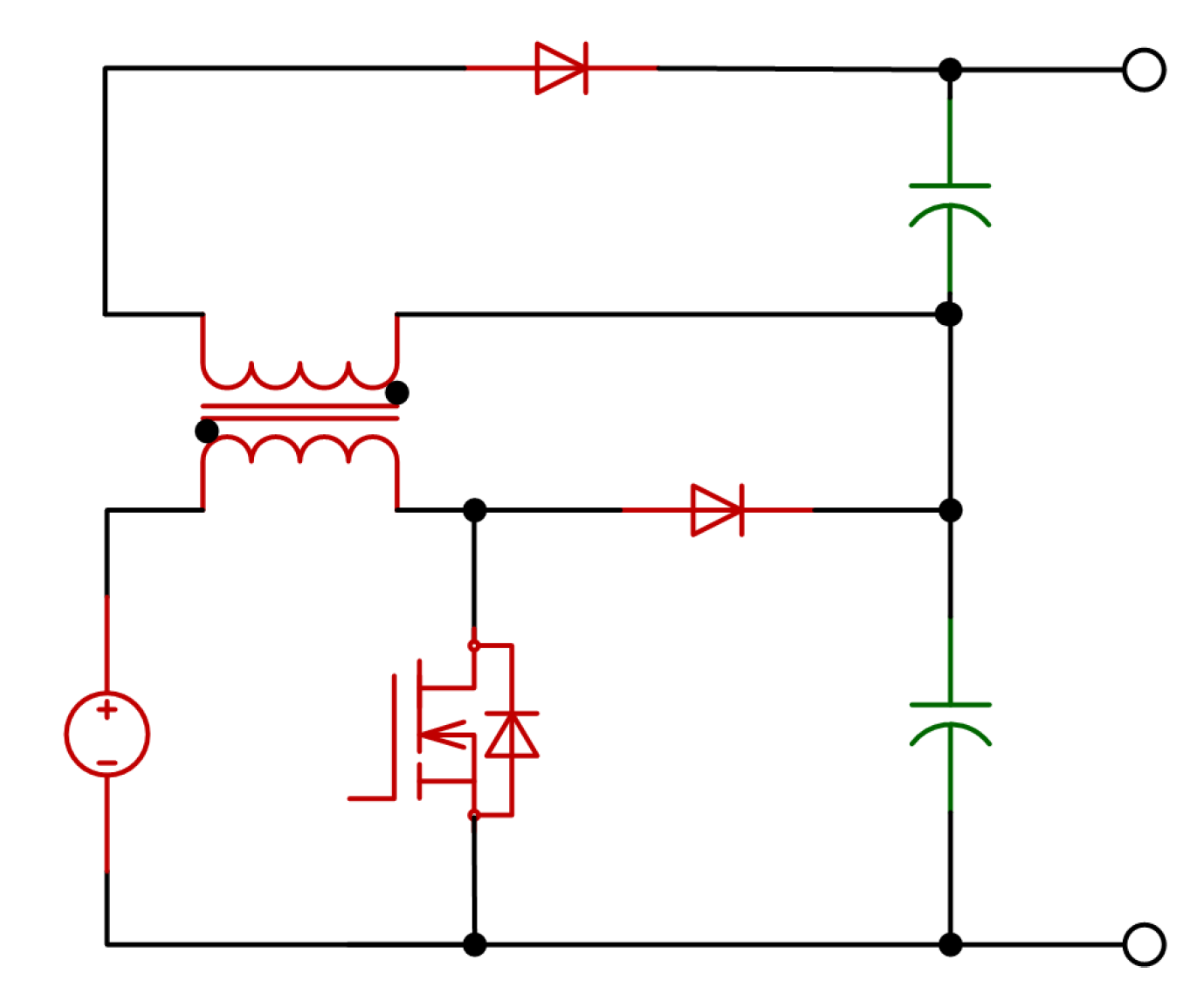
Trying to deal with the DC-link voltage level issue, a boost grid-tie inverter is simulated and tested in [23], where the voltage gain is shared between both the rectifier and the proposed inverter. Grid-tie generation can be realized even when the DC-link voltage is lower than the grid voltage. However, in this topology, high power losses and high current stresses may occur, because of the large ripples in the input inductor currents and the bulky output filter.
Owing to all these problems that exist in the boost inverter, many researches on high step-up DC/DC converters have been developed. Currently, efficient technologies including coupled inductor [24,25,26,27,28] and switched capacitor [25,26,29,30,31,32,33] are often adopted to improve the voltage conversion ratio.
In [24,25,26,27], the proposed flyback converter is able to build an additional energy transmission circuit by means of coupled inductors, and can superimpose the output voltage of the additional circuit on that of the main circuit as shown in Figure 7.
Figure 7. The circuit topology of flyback DC/DC converter.
Energies 08 02742 g007
Thus, a relatively high voltage gain can be achieved. This proposed converter is very suitable for high frequency, low power and high step-up voltage gain applications, but it is usually applied in DC/DC cases and needs a cascaded front-stage rectifier to convert the input AC voltage into DC, which may lead to larger losses, lower efficiency and higher cost.
Switched capacitors are also employed frequently in the proposed converters in [29,30,31,32,33]. In Figure 8, as energy snubbers, switched capacitors are able to store and deliver energy from the input source to the output load during one switching cycle, and therefore fulfill high step-up voltage conversion. This technology is widely adopted in many cases, for its light weight and high power density, but its utilization is also generally restrained in DC/DC areas.
Figure 8. The circuit topology of switched-capacitor DC/DC converter.
Energies 08 02742 g008
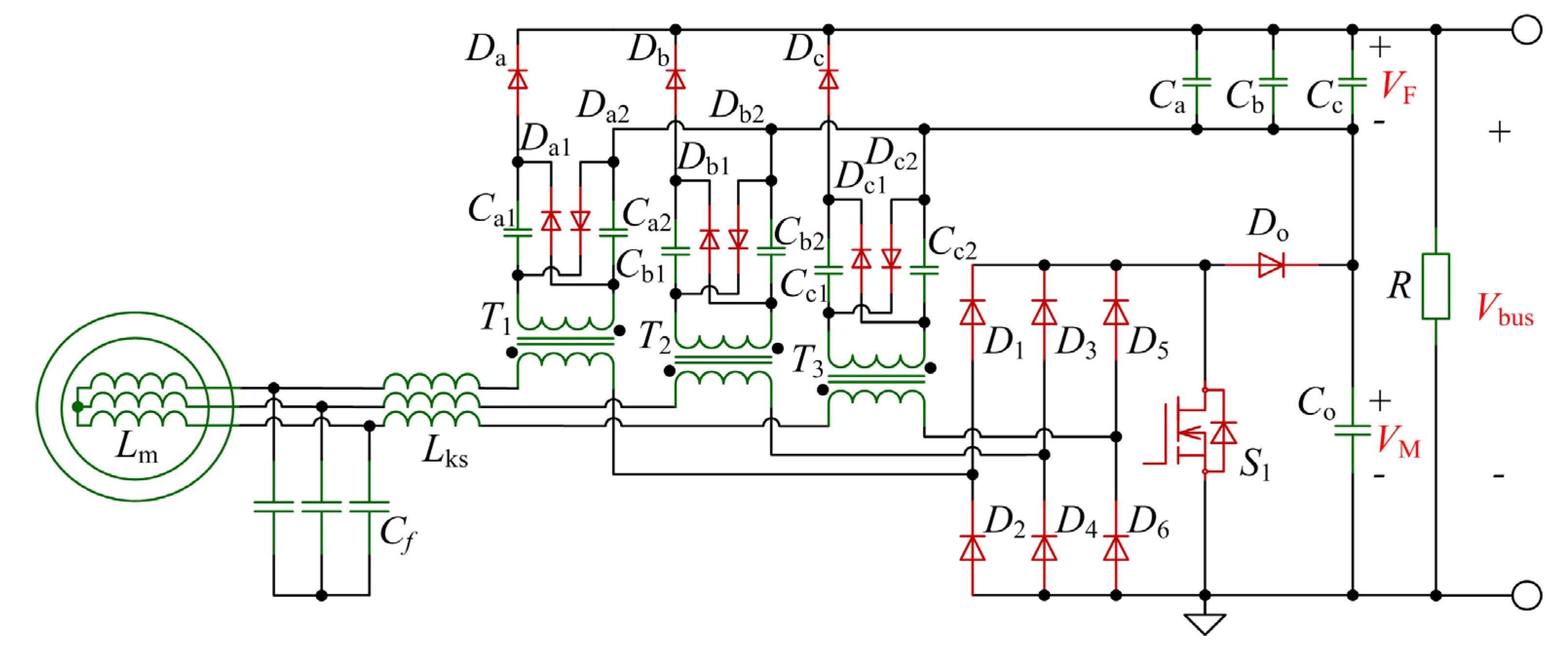
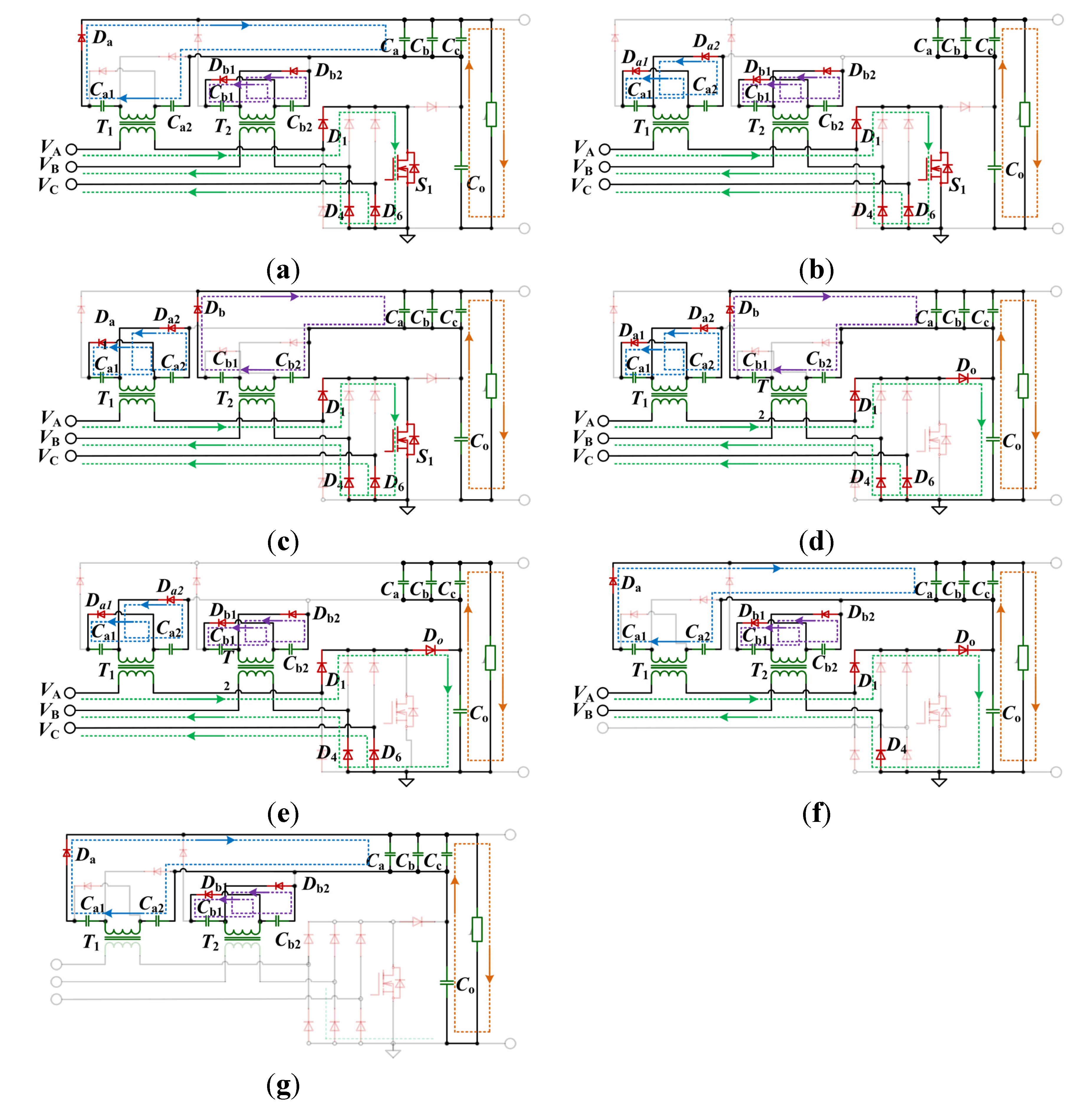
Consequently, in order to solve the problems existing in small-scale WGS, in this paper, a novel three-phase high step-up single stage flyback AC/DC converter with switched capacitors is presented and analyzed. The proposed converter is suitable for urban-roof or power-hungry usage scenarios, and can obtain high voltage gain at low input voltage and high power factor, high efficiency in rated situations. Since it has both rectification and voltage gain improvement functions, no additional DC/DC converter is needed any longer. The input current is designed to be operated in discontinuous current mode (DCM), and inherent power factor correction (PFC) is also achieved at full load. In addition, no electrolytic capacitor is employed, thus the proposed converter can also collect weak power and has a reduced volume.

2. Circuit Configuration

The topology of the proposed converter is presented in Figure 9. By integrating the three-phase single-switch boost circuit and flyback circuits with switched capacitors, the converter can obtain a high voltage gain at low input voltage. The converter is totally divided into four main parts including high frequency filter capacitors Cf, uncontrolled diode bridge rectifier D1 ~ D6, flyback cells and a boost cell (Lks, S1, Do and Co). Moreover, for the purpose of tracking the maximum wind power, a variable step size algorithm is adopted [34,35]. The control strategy will be analyzed in detail in further work, and this paper mainly focuses on the topology of the proposed converter.
The diode bridge will rectify the input AC current to DC at first, and then the boost cell is able to boost the rectified voltage as the output voltage of boost cell VM. In flyback cells, since each unit is completely symmetrical, we take phase A for example to explain the configuration of the cells. In phase A, the flyback cell is composed of transformer T1, diode Da, output capacitor Ca and a switched capacitor cell consisting of capacitor Ca1, Ca2 and diode Da1, Da2. Switched capacitors can store the energy delivered from primary side of T1 when the power switch S1 turns on, and releases it to charge flyback output capacitor Ca through Da when S1 turns off. As a consequence, T1 is able to transform power from primary side to secondary side during the entire switching period. Lkt, which is defined as the leakage inductor of T1, connects the boost inductor Lks serially, and their sum (Lkt + Lks) can be regarded as the equivalent leakage inductor Lk.
Figure 9. The circuit topology of the proposed converter.
Energies 08 02742 g009
In order to further improve the performance at low input voltage, all of the flyback output capacitors Ca, Cb, Cc and the boost output capacitor Co employ film capacitors with small capacitance and small volume instead of electrolytic capacitors. On one hand, by doing so, the converter can prevent the large current leakage and large losses introduced by electrolytic capacitors, and thus can achieve weak energy collection. On the other hand, the adoption of film capacitors can also lead to larger voltage ripples, since the capacitance is small. To restrain the voltage ripples, Ca, Cb, Cc are designed to connect in parallel, for the reason that the ripple of each phase is identical in amplitude and 120° behind sequentially in phase and will weaken each other. CF, which consists of Ca, Cb, Cc, is defined as the equivalent flyback output capacitor and connects Co serially. As a result, the voltage gain is further improved, because the flyback output voltage VF is superimposed to the boost output voltage VM.
The comparison among the proposed AC/DC converter and other three-phase AC/DC converters are made as manifested in Table 1. According to the table, although the proposed converter has the maximum quantity of power switches and diodes, the unit-price of the chosen auxiliary diodes in flyback cells is exceedingly low (ES3G, less than $0.05/pieces). Moreover, some traditional converters even need low-frequency transformers to achieve high voltage gain, which will further increase the converter cost. With a relatively low cost and good performance, the proposed AC/DC converter is competitive in small-scale WGS applications.
Table 1. Cost Comparison.
AC/DC ConverterHigh Frequency Transformer/InductorPower Switch QuantityPower Diode QuantityAuxiliary Diode QuantityCost
Diode Bridge + Boost Converter1170Lowest
PWM Converter3600High
Matrix Converter3900Highest
Three-phase Single-switched Converter3170Low
Proposed Converter3179Low

3. Operation Principles

3.1. Operation States

In this section, operating modes are analyzed in detail. To simplify the circuit analysis, several assumptions are made:
(1)
All three flyback cells are symmetrical, and the corresponding components in each phase are identical.
(2)
Switch S1 and all diodes are regarded as ideal components.
(3)
VF, VM and input voltages are constant during a whole switching period.
From Figure 10, it can be seen that the 2π input voltage cycle can be divided into 12 symmetrical intervals.
Figure 10. The waveform of the input voltage.
Energies 08 02742 g010
In each interval, the calculation methods are similar, so only take time interval within [π/2, π/3] of phase A for instance to analyze the proposed circuit. The relationship of input voltage within this interval is:
V A > | V B | > | V C | > 0 > V C > V B
Since the average input voltage of VC is very low in this interval, the impact caused by the flyback cell of phase C can be neglected and the circuit is assumed to be only influenced by that of phases A and B. The change rates of secondary current iPA and iPB of transformer T1 and T2 can be obtained as:
d i P A d t + d i P B d t = 0
In steady state, an entire switching period can be mainly divided into seven modes. Typical waves are presented in Figure 11 and equivalent circuit of each mode is shown in Figure 12. In Figure 11, vGATE represents the control signal of switch S1, iA, iB and iC represent the input current, and uCA is the voltage across the switched capacitor Ca1/Ca2.
Figure 11. Key waveforms of the proposed converter.
Energies 08 02742 g011
Figure 12. Equivalent circuits. (a) mode I; (b) mode II; (c) mode III; (d) mode IV; (e) mode V; (f) mode VI; (g) mode VII.
Energies 08 02742 g012
Mode I (t0 ~ t1). According to Figure 12a, switch S1 turns on at the beginning of this mode, and diode D1, D4, D6 are forward-biased. Flyback cells have only two working states. In phase A, diode Da conducts, and the switched diode Da1 and Da2 are reverse-biased. Switched capacitor Ca1 and Ca2 in series with the secondary inductor of transformer T1 charges the flyback output capacitor CF (State-OFF). In phase B, diode Db is reverse-biased and switched diode Db1 and Db2 are forward-biased. Power supplied by transformer T2 flows through Db1/Db2 to charge switched capacitor Cb1/Cb2 (State-ON). As a result, iA starts to increase from zero and iB, iC also rise in the opposite direction. This mode ends when iPA falls down to zero.
Mode II (t1 ~ t2). As shown in Figure 12b, flyback cell in phase A turns to State-ON. Current iPA begins to increase, while iPB is decreasing. This transition interval is finished, when iPB reaches zero at t2.
Mode III (t2 ~ t3). From Figure 12c, flyback cell of phase B is under State-OFF. The input source stores its energy into the equivalent leakage Lk and the magnetizing inductor LM of T1. Current iA, iB and iC keep increasing from their initial mode value and iPA, iPB increase as well. Until the moment t3, S1 turns off and this mode comes to the end.
Mode IV (t3 ~ t4). From Figure 12d, this mode starts when S1 turns off and diode Do, D1, D4, and D6 are forward-biased. The states of flyback cells stay the same with Mode III. The input sources in series with inductors Lk and LM charges the boost cell output capacitor Co. Since the voltage across Co is higher than the input voltage, iA, iB, iC and iPA, iPB decrease rapidly. This mode ends when iPB reaches zero at t4.
Mode V (t4 ~ t5). According to Figure 12e, this interval is also a transition mode. Flyback cells of phase A and B are both under State-ON. Current iPB starts to rise, while iPA is still abating. This mode ends when iPA equals to zero at t5. At this time iC also drops down to zero.
Mode VI (t5 ~ t6). From Figure 12f, iC remains zero and diode D6 turns off. Flyback cell of phase A is under State-OFF and that of phase B turns to State-ON. The input source of phase A and B keep charging Co with inductors Lk and LM. Current iA and iB continue to drop until they reach zero at t6 simultaneously, and at this moment Mode VI is finished.
Mode VII (t6 ~ t7). It can be seen in Figure 12g, diode D1, D4 and Do turn off and the states of flyback cells do not change. Inductor LM of T1/T2 alone transfers power from the primary side to the secondary side. Current iA, iB, iC maintain zero, and iPA, iPB reduce slowly. This mode ends when S1 is turned on again at the moment t7, and the entire switching period is ended.

3.2. Operation Analysis

According to the operation states and the equivalent circuits of the proposed converter, expressions of each mode are obtained, so that parameters of the converter can be optimized. Since Mode II and Mode V are transition modes and have little influence on the converter, they are neglected in order to simplify the circuit analysis. Parameters are defined as follows: iLmA represents the magnetizing current of phase A; IPAx, UCAx and ILmAx(x = a, b, c, d, e) are defined as the initial value of corresponding mode of parameter iPA, uCA and iLmA; VLmA is the voltage across the magnetizing inductor of T1; C represents the capacitance of Ca1/Ca2.
From Figure 12a, equations of Mode I is listed as:
{ V A = V LmA + L k d i A d t i A = i LmA + N i PA i PA = C d u CA d t V F = 2 u CA N V LmA V LmA = L M d i LmA d t
By solving Equation (3), expressions of key parameter uCA and iPA is calculated as:
{ u CA ( t ) = K a1 + K a2 β t + V F 2 + N L M 2 ( L k + L M ) V A i PA ( t ) = C K a1 β 2 t + C K a2 β
In Equation (4), Ka1, Ka2 represent the mode coefficients of Mode I, and β is defined as the equivalent mode angular frequency:
{ u CA ( t ) = K a1 + K a2 β t + V F 2 + N L M 2 ( L k + L M ) V A i PA ( t ) = C K a1 β 2 t + C K a2 β
β = 2 ( L k + L M ) N 2 C L M L k
The mode duty cycle da can be achieved as Equation (7), where Ts is the switching period and IPB0 represents the initial value of Mode I:
d a = I PB0 T S C K a1 β 2
IPB0 can be approximately obtained as:
I PB0 I PA1 I PA0
By adopting similar approach, the mode expressions and the duty cycle of each mode can be obtained as well.
In Mode III, uCA and iPA are:
{ u CA ( t ) = K b1 cos ( α t ) + K b2 sin ( α t ) + N L M L k + L M V A i PA ( t ) = 2 C K b1 α sin ( α t ) + 2 C K b2 α cos ( α t )
Equivalent mode angular frequency α and mode coefficients Kb1, Kb2 are described as:
{ K b1 = U CA1 N L M L k + L M V A K b2 = I PA1 2 C α
α = L k + L M 2 N 2 C L M L k
The duty cycle of Mode III is:
d b = D d a = D I PB0 T S C K a1 β 2
In Mode IV, uCA and iPA are:
{ u CA ( t ) = K c1 + K c2 α t + N L M L k + L M ( V A 2 3 V M ) i PA ( t ) = 2 C K c1 α 2 t + 2 C K c2 α
Mode coefficients Kc1, Kc2 are described as:
{ K c1 = U CA2 N L M L k + L M ( V A 2 3 V M ) K c2 = I PA2 2 C α
The duty cycle of Mode IV is:
d c = K c2 T s K c1 α
In Mode VI, uCA and iPA are:
{ u CA ( t ) = K d1 cos ( β t ) + V F 2 + N L M ( V A V B V M ) 4 ( L k + L M ) i PA ( t ) = C K d1 β sin ( β t )
Mode coefficient Kd1 is described as:
K d1 = U CA3 V F 2 N L M ( V A V B V M ) 4 ( L k + L M )
The duty cycle of Mode VI is:
d d = I LmA3 2 K d1 N L M + V A V B V M 2 ( L k + L M ) N C K d1 β 2 1 T S
In Mode VII, uCA and iPA are:
{ u CA = K e1 cos ( θ t ) + K e2 sin ( θ t ) + V F 2 i PA = C K e1 θ sin ( θ t ) + C K e2 θ cos ( θ t )
Equivalent mode angular frequency θ and mode coefficients Ke1, Ke2 are described as:
{ K e1 = U CA4 V F 2 K e2 = I PA4 C θ
θ = 2 N 2 C L M
The duty cycle of Mode VII is:
d e = 1 D d c d d
Although the mode states and expressions have already been analyzed, the numerical solution of the key parameters still cannot be achieved, as additional equations must be found. Since the output voltage of flyback cell VF and that of boost cell VM are regarded as constant values, the ampere-second balance principle of capacitor is adopted as:
{ 0 d c T S i A d t   +   0 d d T S i A d t  =  0 T S i o d t 0 d b T S i PB d t + 0 d d T S i PB d t + 0 d d T S i PA d t                 + 0 d e T S i PA d t + 0 d a T S i PA d t = 0 T S i o d t
Where io and iPB can be described as Equation (24) and Vbus is the total output voltage of the circuit:
{ i o = V bus R = V F + V M R i PB i PA i o
Combining and solving these mode expressions and Equations (23) and (24), finally the numerical solution of the main parameters is obtained.

3.3. Parameter Design

Since the proposed converter is applied in small-scaled WGS, two requirements must be met to guarantee normal operation:
(1) When the input voltage is very low, high voltage gain is the main optimized purpose, because a relatively high output voltage is needed to act as the supply of the post-stage inverter for further grid-tie generation. Define Mgain as the voltage gain as Equation (25), where Vin_p represents the RMS value of the input phase voltage:
M gain = V bus V in_p
Based on the calculation results, the voltage gain Mgain is primarily decided by parameters of transformer turns ratio N, equivalent leakage inductor Lk and duty cycle D. To further illustrate the influence on Mgain caused by N, Lk and D, Figure 13 is drawn, where Figure 13a–c represents the relationship among Mgain and Lk, D, when N is equal to 1, 3 and 5.
As it is shown, a larger D and a smaller Lk lead to a higher Mgain, namely when a high voltage gain is needed at low input voltage, a large duty cycle and a small equivalent leakage inductor should be chosen to satisfy the demands. Accordingly, the value range of small duty cycle or large leakage inductor should be abandoned. However, extremely high D or extremely small Lk may result in low efficiency, and should be prevented also.
Figure 13. Relationship of Mgain and N, D, Lk. (a) case of N = 1; (b) case of N = 3; (c) case of N = 5; (d) case of chosen area.
Energies 08 02742 g013
Thus, in Figure 13d, the relationship of Mgain and N, Lk, D within a reasonable limited value range, which covers a relatively high D and a small Lk area, is shown. Obviously, both the voltage gain of N = 3, Mgain (N = 3) and that of N = 5, Mgain (N = 5) are higher than that of N = 1, Mgain (N = 1). When D is relatively high and Lk is small, Mgain (N = 3) is slightly larger than Mgain (N = 5), and when D is reduced, Mgain (N = 3) is lower than Mgain (N = 5). Therefore, Mgain (N = 3) is more suitable for the proposed converter, since a larger Mgain at high D is needed at low input voltage, and a limited Mgain at relatively low D to ensure normal operation.
(2) When the input voltage is in the rated situation, instead of pursuing high voltage gain, high conversion efficiency is of the greatest importance in the proposed converter. Moreover, sinusoidal input current waves in phase with the input phase voltages are also needed to ensure a high power factor. At this time, the input voltage has increased to a high level, and a medium voltage gain is enough for the requirement of DC-link. Thus, a very large Mgain is unnecessary. Although flyback cells contribute to high voltage gain at low input voltage, they would also introduce distortions into the input current, and consequently reduce the conversion efficiency. It is for the reason that along with the increase of the flyback output voltage VF, the secondary current of the transformers ipA, ipB and ipC will also get larger and larger as the result. The secondary currents will lead to a growing influence on the primary side input current iA, iB and iC respectively and cause distortions. Define MFM as the distortion factor as Equation (26), where VF is the output voltage of flyback cells and VM is that of the boost cell:
M F M = V F V M
From Equation (26), it can be seen that the larger the MFM is, the greater proportion VF possesses in the total output voltage of the converter Vbus (Vbus = VF + VM), and thus the greater the distortions of input currents are. The influence on the input current caused by MFM is presented in Figure 14.
Figure 14. Influence on the input current by MFM.
Energies 08 02742 g014
The distortion factor MFM is also decided by parameter N, D and Lk. Their relationships are presented in Figure 15, where Figure 15a–c illustrates the varying trends of different turns ratios (N = 1, 3 and 5).
Figure 15. Relationship of MFM and N, D, Lk. (a) case of N = 1; (b) case of N = 3; (c) case of N = 5; (d) case of chosen area.
Energies 08 02742 g015
As shown, when Lk is constant and along with the increase of D, MFM will rise up at the beginning until reaching its peak at around D = 0.6 and then fall down. At the same time, when D is constant, MFM will present a growing trend if Lk keeps decreasing. According to the previous analysis, low MFM is demanded, and by choosing a large Lk, the converter can obtain high efficiency at rated input voltage as shown in Figure 15a–c, but a large Lk will contradict the requirement of high Mgain. Consequently, a suitable MFM range should be found instead of adopting the MFM as large as possible. Figure 15d shows the comparison of different turn ratios (N = 1, 3, 5) in the same area as chosen by Figure 13d. It is shown that MFM of N = 1, MFM (N = 1), varies slightly and keeps its value around 0.4, which is larger than that of N =3, MFM (N = 3), and N = 5, MFM (N = 5) when Lk varies from 15 to 30 μH. Moreover, Mgain (N = 1) is also small and can’t provide a high enough voltage gain, thus MFM (N = 1) should not be accepted. MFM (N = 5) remains smaller than MFM (N = 3) in the chosen area and seems to have a better performance when the input voltage is at rated. However, under the condition of MFM (N ≥ 5), VF is much smaller than VM and the function of flyback cells can be neglected. Characters of the proposed topology are almost the same with that of the three-phase single-switch boost converter. This is because the secondary transformer currents ipA, ipB and ipC are N times smaller than that of primary sides, which are limited by the input currents iA, iB and iC as:
N i Px = i x i Lmx < i x    (x=A, B, C)
If N is larger, the iPx is tends to be very small, and thus the flyback cells seems not to function at all and can be neglected. Moreover, if a certain Lk value is given, the input current peak of MFM (N = 5) is always higher than that of MFM (N = 3) under the case of identical input voltage, voltage gain Mgain and thus identical output power, which is shown in Figure 16. Higher current peak often means higher current stress, higher power loss and lower efficiency, which is against to the optimization objective, so MFM (N = 3) is selected instead of MFM (N ≥ 5). What’s more, the traditional three-phase single-switch Boost converter can also obtain high voltage gain through adopting very small boost inductors, but its input current peak is much higher than the proposed converter as well.
Figure 16. Comparison of input current peaks.
Energies 08 02742 g016
As a result, the main optimization purpose can be described as follows: when low input voltage is supplied, in order to provide an adequate DC-link voltage level, obtaining high voltage gain is the primary design goal; when input voltage is at rated levels, the primary objective is to guarantee high efficiency and sine-shaped input current waveforms, because at this moment no extremely high voltage gain is needed and the DC-link voltage should be maintained within a normal operation range. Since the variation trend of Mgain and MFM are not same, a trade-off optimized parameters should be given to meet both of the demands for efficiency and voltage gain: a voltage gain larger than 12 is required when the input voltage is low, and MFM is designed to be lower than 0.4. According to Figure 13d and Figure 15d, Lk should be designed within 15 ~ 20 μH to achieve high voltage gain of 8 ~ 18, and low distortion factor of 0.1 ~ 0.4. The appropriate parameters are selected and presented as shown in Table 2.
Table 2. Main parameters of the proposed converter.
ParametersValue
Filter Capacitors Cf0.32 μF
Switched Capacitors Ca1/Ca22 μF
Flyback Output Capacitors Ca40 μF
Boost Output Capacitors Co40 μF
Equivalent Leakage Inductor Lk18 μH
Turn Ratio N3
Load Resistance R440 Ohm
Switching Frequency fS100 kHz
For further analysis, the relationship of MFM, Mgain, MF and MM against D for Lk = 18 μH is given in Figure 17, where Mgain, MF and MM are the voltage gain of VF, VM and Vbus. MFM reaches its peak value 0.35 at D = 0.6. Voltage gain Mgain is larger than 12 when D is higher than 0.6, which is well suitable for the optimization design.
Figure 17. Relationship of MFM and voltage gain of VF, VM and Vbus against D at Lk = 18 μH.
Energies 08 02742 g017

3.4. Power Devices Selection

3.4.1. Power Switch and Diode Selection

The power devices are selected according to the rated power (400 W). Based on the calculation result from mode expressions and Equations (23) and (24), the maximum current and voltage of the power devices at rated are obtained and presented in Table 3. For safety consideration, 1.5 times current/voltage margins are also provided. The types of the devices are also given in Table 3.
Table 3. Power devices selection.
ComponentsCalculated Max Instantaneous CurrentCalculated Max Instantaneous VoltageSelected Devices
Power Switch16 A350 VFCH47N60N
Power Diode16 A350 VBYC30-600P
Auxiliary Diode1.7 A12 VES3G

3.4.2. Transformer Design

According to the analysis in Section 3.2, the transformer turns ratio N = 3 is chosen. The turns of the primary side of the transforms n1 can be calculated as:
n 1 = j A w k w I in_max
Parameter j = 3.5 A/mm2 represents the maximum current density, Aw is the winding area of the core, kw = 0.3 is the winding factor and Iin_max = 6.75 A represents the maximum input current at rated power. The transformer cores are designed as PC-40 PQ26/25, and from the datasheet, the Aw = 84.5 mm2 is obtained. As a result, n1 = 13.1 is calculated and chosen as 14 turns. The secondary side turns n2 = 42 turns is also calculated.

3.5. Power Losses Estimation

Power losses should be estimated so that the conversion efficiency can be seen. The power losses include power switch S1 loss, uncontrolled diode bridge rectifier D1 ~ D6 losses, diode Do loss, transformer losses and power losses of the flyback cells.

3.5.1. Uncontrolled Diode Bridge Rectifier D1 ~ D6

In order to estimate the power loss of the diode bridge rectifies, the average current through each diode should be found as Equation (29), where IDTs, ipeak_A, ID1 and PD1 represent the average current of D1 in one switching period, peak value of iA in one switching period, average current of D1 and power loss of D1 respectively:
I DTs = 1 T S 0 ( 1 d e ) T S i D1 d t = 1 T S 0 ( 1 d e ) T S i A d t
Equation (29) can be approximated as:
I DTs 1 T S i peak_A 2 ( 1 d e ) T S = ( 1 d e ) 2 i peak_A
Where ipeak_A can be further approximated as:
i peak_A V A sin ω T L k D T S
Therefore, ID1 is estimated as:
I D1 = 1 2 π 0 π V A sin ω T L k D T S ( 1 d e ) 2 d ω T = V A T S 2 π L k D ( 1 d e )
The power loss of D1 can be expressed as Equation (33), where Vforward is the forward voltage of the chosen diode BYC30-600P:
P D1 = I D1 V forward
Thus, the power loss of the diode bridge rectifier is achieved as:
P DioBri = n P D1 = 9.67 Watt

3.5.2. Diode Do

Similarly, the average current of Do is estimated as:
I Do = 6 × 1 2 π π 3 2 π 3 V A sin ω T L k D T S ( d c + d d ) 2 d ω T = 3 V A T S 2 π L k D ( d c + d d )
The power loss of diode Do is expressed as:
P Do = I Do V forward = 1.21 Watt

3.5.3. Power Switch S1

The average current of S1 is estimated as:
I S1 = 6 × 1 2 π π 3 2 π 3 V A sin ω T L k D T S D 2 d ω T = 3 V A T S 2 π L k D 2
In the proposed converter, the type of S1 is FCH47N60N, and its forward voltage is VSforward. The power loss of S1 is:
P S1 = I S1 V Sforward = 3.25 Watt

3.5.4. Flyback Cells

The flyback cell losses are made up of switched capacitors losses and diode Da (Db, Dc) loss, where all the diodes are ES3G.
The average current of switched capacitor Da1 is estimated as:
I Da1 = 1 π 0 π i PA_peak 2 ( D + d c ) d ω T
The power loss of Da1 is:
P Da1 = I Da1 V FBforward = 0.3 Watt
The average current of Da is:
I Da = 1 π 0 π i PA_peak ( d d + d e ) d ω T
The power loss of Da is:
P Da = I Da V FBforward = 0.32 Watt
Consequently, the total losses of the flyback cells can be expressed as:
P FlyBack = 3 × ( P Da + 2 P Da1 ) = 2.76 Watt

3.5.5. Transformers

Besides power dissipated from winding resistance, the power losses of transformers also include core losses. The transformer cores are designed as PC-40 PQ26/25, where Ve = 6,530 mm3. According to the datasheet, the core loss per volume, Pcv = 0.0004 W/mm3 at 60 °C. As a result, the core loss is:
P core = V e P cv = 2.61 Watt
The average current of iA during one switching period can be expressed as:
I A = V A T S π L k D ( 1 d e )
The RMS value of iA is:
I A_RMS = I A 0.45
The copper loss is:
P copper = I A_RMS R Trans = 9.12 Watt
RTrans (=0.4 Ω) represents the equivalent winding resistance of the transformer. The total power losses of the transformers can be calculated as Equation (48):
P Trans = 3 × ( P core + P copper ) = 35.19 Watt
Finally, the conversion efficiency at rated condition (400 W) can be achieved as Equation (49):
η % = P rated P rated + P DioBri + P Do + P S1 + P FlyBack + P Trans × 100 % = 87.97 %
Power losses of each part are summarized in Table 4.
Table 4. Power losses summary.
ComponentsPower Losses (Watt)
Rectifier Bridge D1 ~ D69.67
Diode Do1.21
Power Switch S13.25
Flyback Cells2.76
Transformers35.19
From the table, it is seen that the most influential factor reducing the conversion efficiency is the copper losses of the transformers, because a large equivalent winding resistance RTrans is introduced into the converter. For the purpose of improving the efficiency, modified transformers with small winding resistance should be employed in the next step.

4. Experimental Results

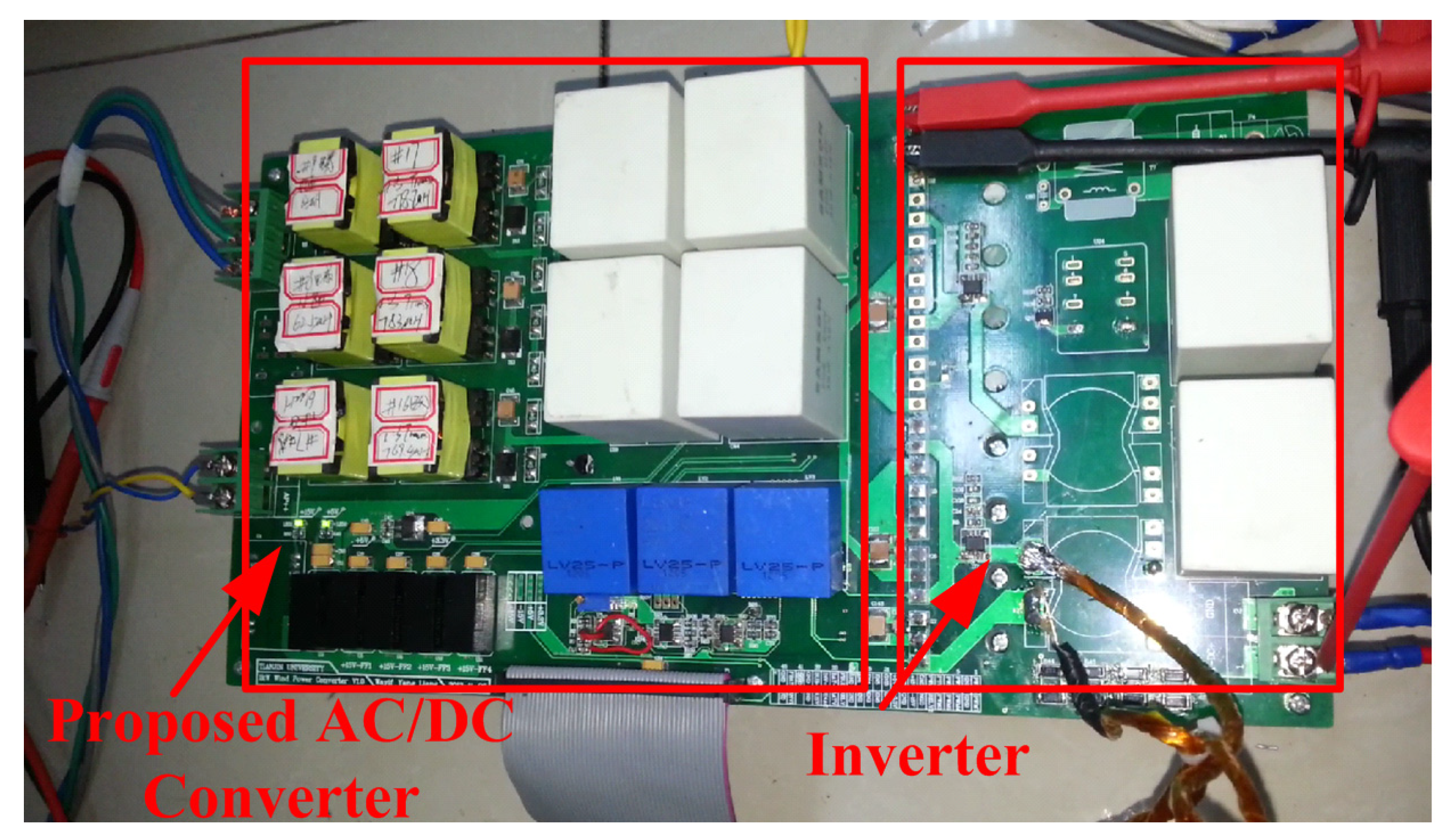
In order to verify the feasibility of the proposed converter, a 400 W prototype was made and shown in Figure 18. A front-stage PMSM is employed as the power supply. The PMSM can output a rated phase voltage of 48 V AC at its rated wind speed of 12 m/s. To match up with the voltage level of the PMSM, the proposed converter is designed to operate with rated input phase voltage of 48 V AC. Besides, the DC-link voltage is required to be maintained at around 410 ~ 430 V DC, so that the post-stage inverter is able to fulfill grid-tie generation. Consequently, a voltage gain of 9 is demanded under rated condition and the correspondent duty cycle D is set as 0.45 according to Figure 17.
Figure 18. The proposed converter prototype.
Energies 08 02742 g018
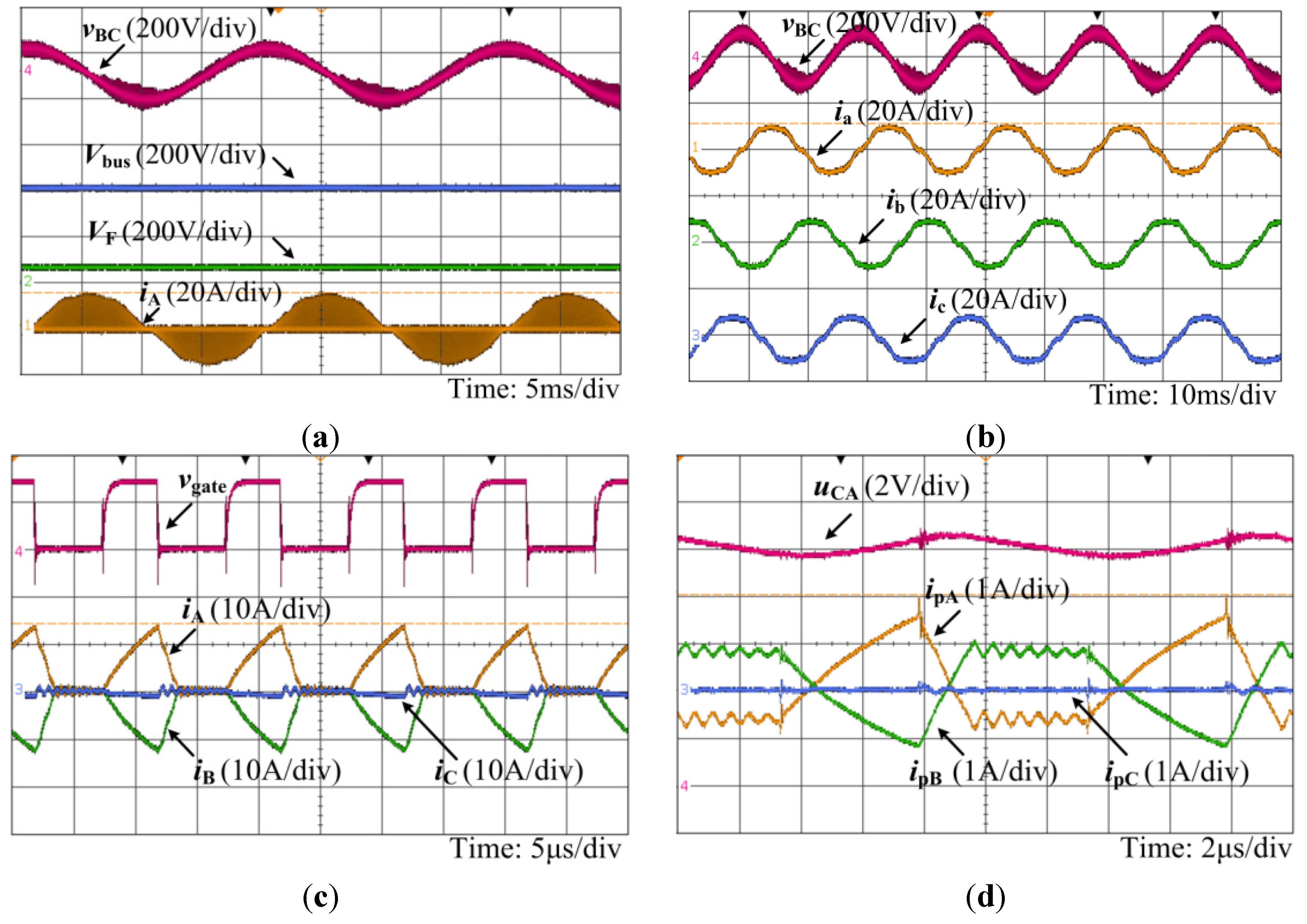
The experimental results under the rated conditions are shown in
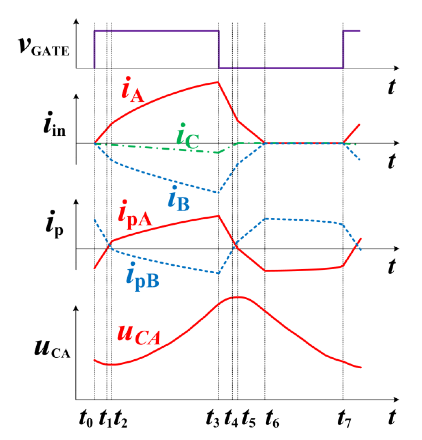
 Figure 19. In Figure 19a, line voltage between phase B and C vBC, total output voltage Vbus, flyback output voltage VF and input current iA are presented, where Vbus is 420 V, VF is 80.7 V, and the input phase voltage Vin-p is 45 V AC. The voltage gain Mgain is calculated as 9.32, which matches well with the aforementioned demand. Moreover, the distortion MFM is limited to 0.24, so the envelope waveform of iA exhibits a sine-shaped waveform. Figure 19b shows the PMSM output currents ia, ib and ic, where only small distortions exist in the waveforms and the THD is 7.4%. Figure 19c shows the control signal vgate and the input currents iA, iB and iC in several switching cycles. At this time, since MFM is limited and the distortion introduced by flyback cells is restrained, waveforms of current iA, iB and iC are regarded to vary linearly. After rising from zero and reaching their peaks simultaneously, iC drops to zero at first and then iA, iB also fall to zero. Figure 19d illustrates the secondary current of flyback cells iPA, iPB, iPC and voltage across the switched capacitor Ca1/Ca2 uCA. Furthermore, waveforms in Figure 19c,d match well with the theoretical waveforms presented in Figure 11. The main experimental results of the converter are measured as follows: D = 0.45, Vin-P = 45 V AC, VF = 80.7 V, Vbus = 420 V, Mgain = 9.32, MFM = 0.24, THD = 7.4%, PF (power factor) = 0.99, Efficiency η = 87.6%.
Figure 19. Experimental results under the rated conditions. (a) input line voltage, output voltage and input current; (b) input line voltage and PMSM output currents; (c) gate signal and three phase input current in detail; (d) uCA and secondary currents of flyback cells.
Energies 08 02742 g019
The performance at low input voltage is also tested as shown in Figure 20, where each of the waveform represents the same voltage/current signal as that in Figure 19. By introducing the flyback cells and adopting high duty cycle D = 0.7, the proposed converter can achieve high voltage gain at low input voltage. At this time, Vbus is 163 V, VF is 34.6 V and Vin-p is 11.6 V AC. The voltage gain Mgain reaches a relatively high level of 14. Besides, waveforms in Figure 20c,d also match with the theoretical analysis. The main parameters of the converter are measured as follows: D = 0.7, Vin-P = 11.6 V AC, VF = 34.6 V, Vbus = 163 V, Mgain = 14, MFM = 0.27, THD = 8.2%, PF (power factor) = 0.99, Efficiency η = 81.1%.
Figure 20. Experimental results at low input voltage. (a) input line voltage, output voltage and input current; (b) input line voltage and PMSM output currents; (c) gate signal and three phase input current in detail; (d) uCA and secondary currents of flyback cells.
Energies 08 02742 g020
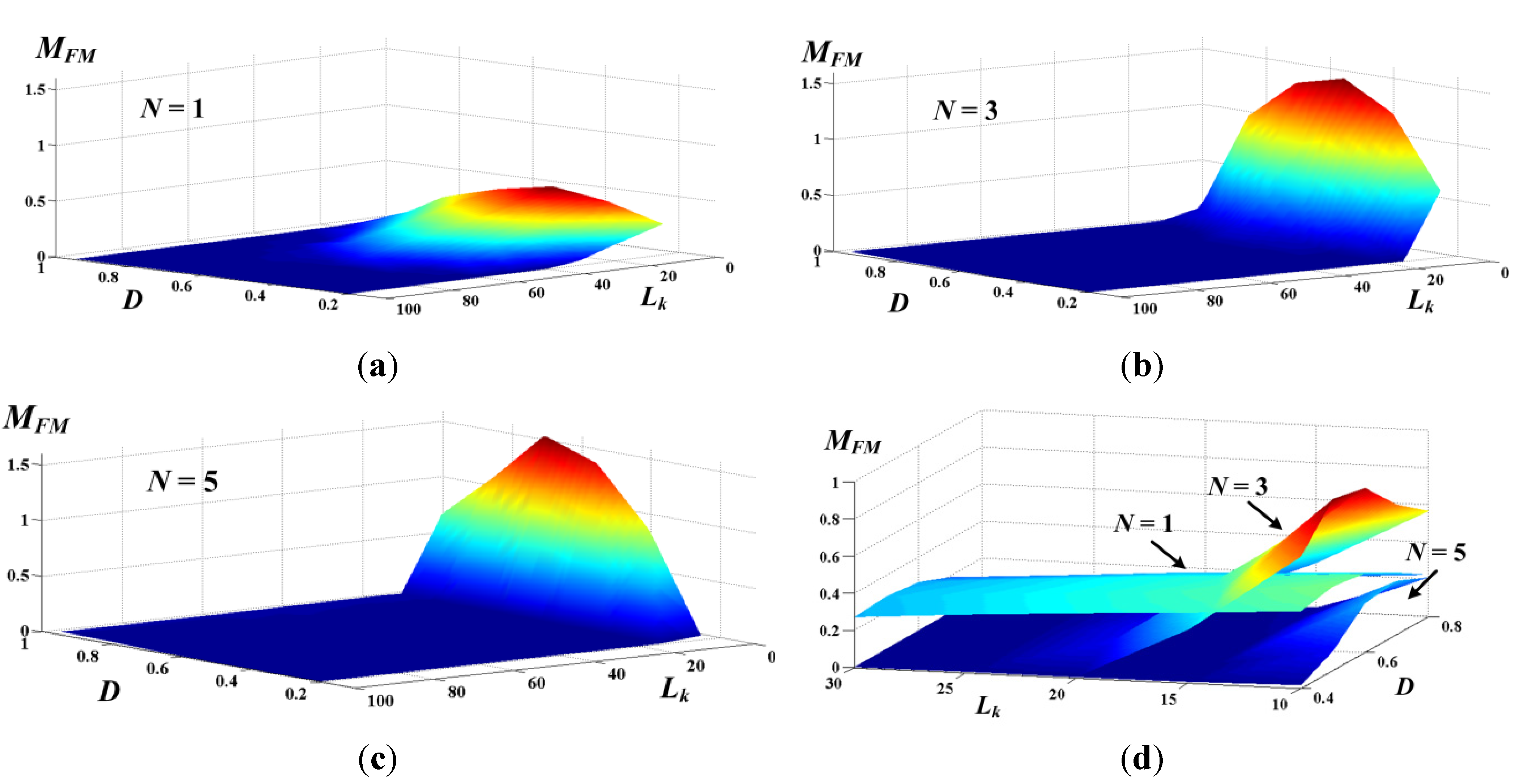
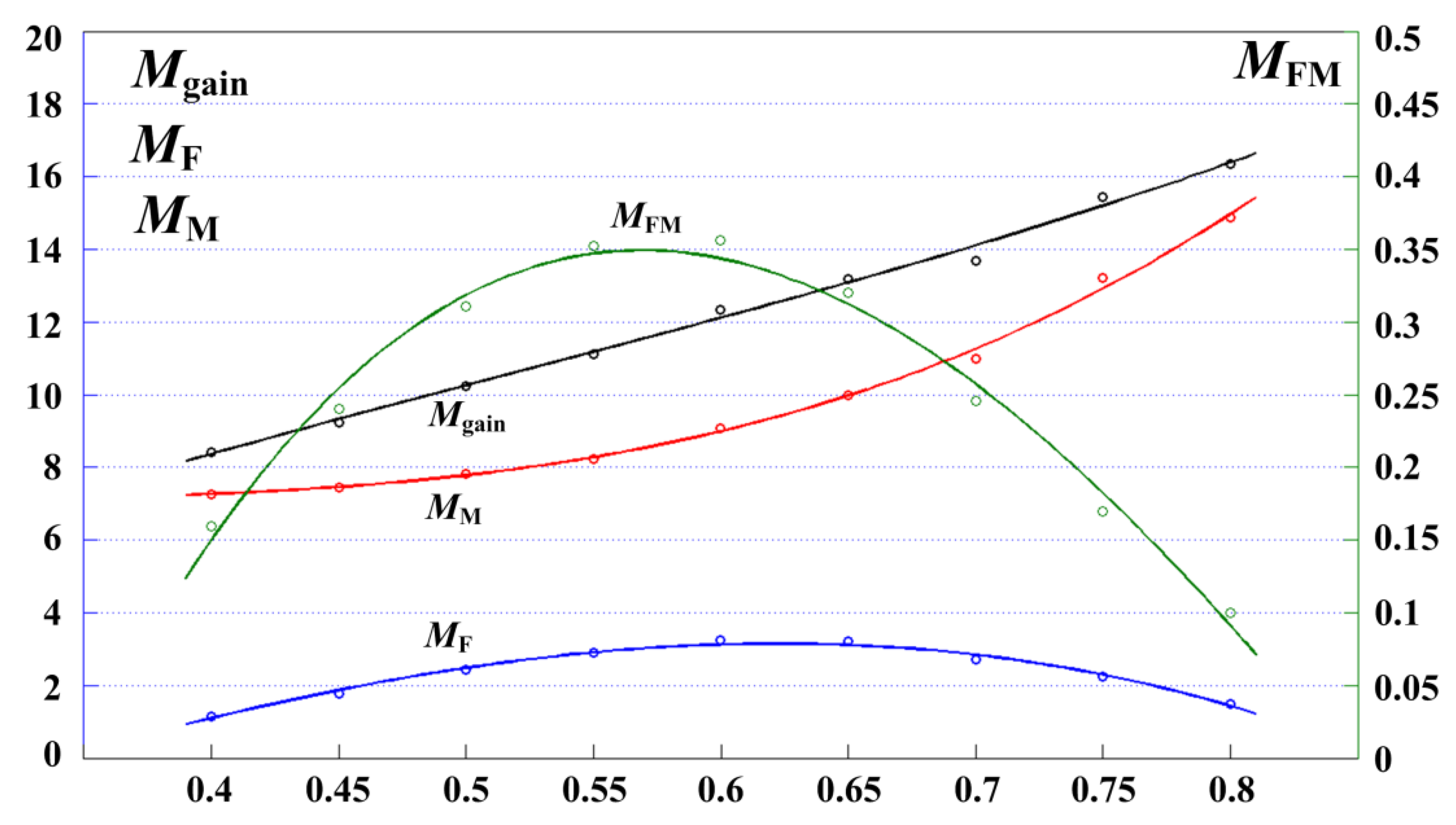
Additionally, as analyzed before, MFM will reach its peak at around D = 0.6 if a constant Lk is set. At the same point, the input current distortion caused by flyback cells will be equal to its maximum value as well. Consequently, if the maximum value of MFM is acceptable, the optimized parameters of the proposed converter can satisfy the design requirements for conversion efficiency. The relevant experiment should be conducted.
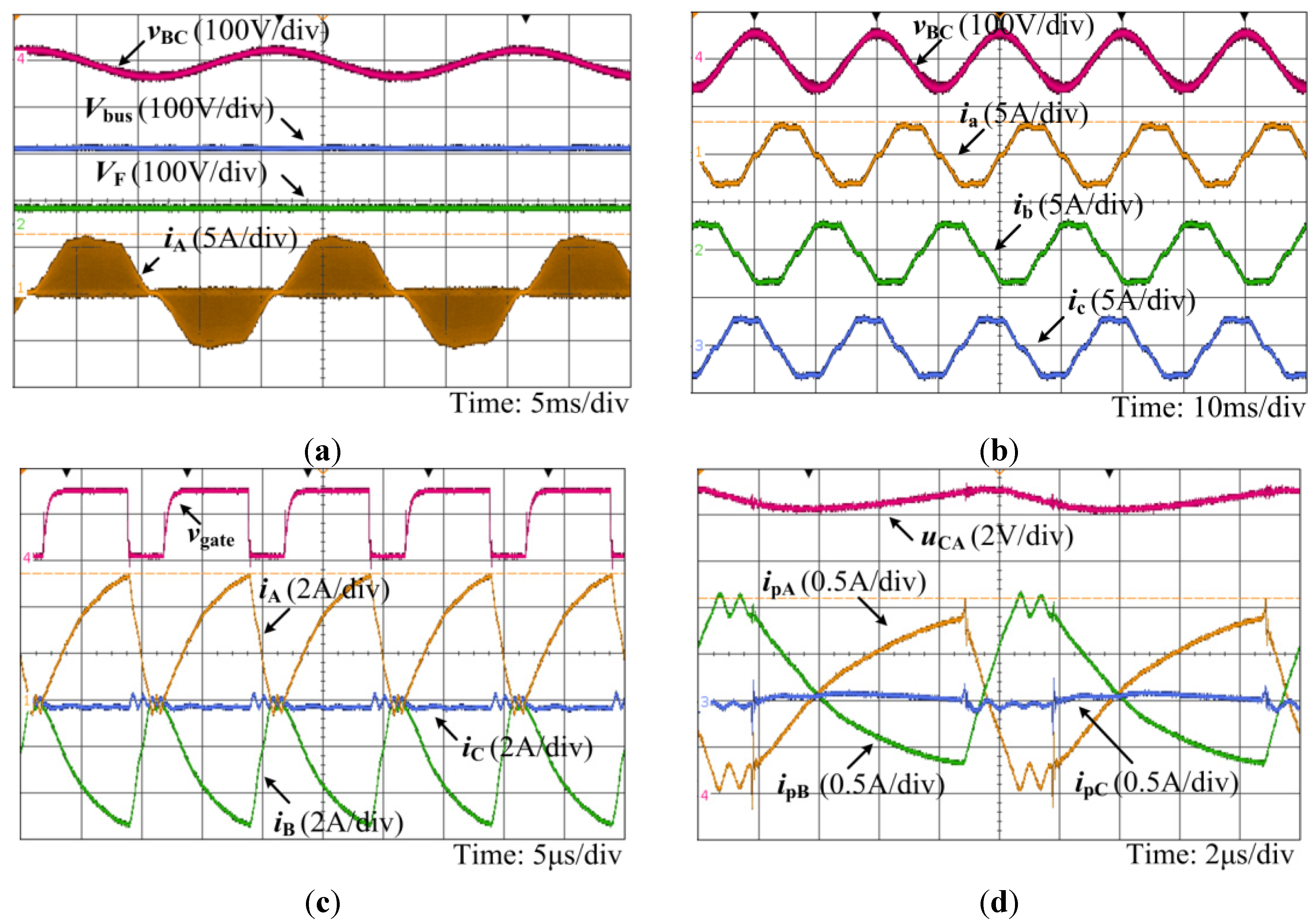
In Figure 21, experimental results under the condition that MFM reaches its peak are presented, where Vbus is 420 V, VF is 108.5 V and MFM is 0.35. As it can be seen from Figure 21a,b, the waveform distortion is obviously larger than that of rated condition. The secondary currents of flyback cells iPA, iPB, 
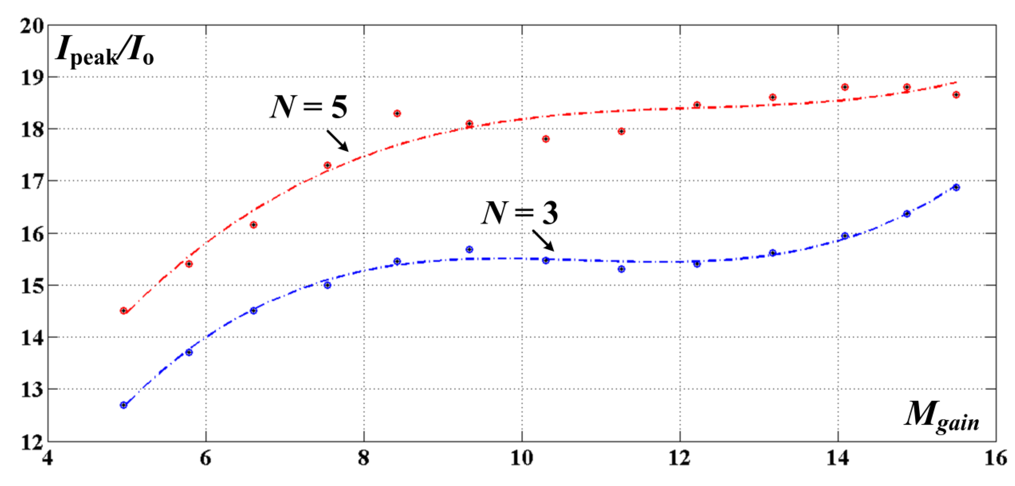
iPC are almost as twice as that of rated condition, which demonstrates the influence caused by flyback cells have been strengthened. The main parameters of the converter are measured as follows: D = 0.6, Vin-P = 34.6 V AC, VF = 108.5 V, Vbus = 420 V, Mgain = 12.1, MFM = 0.35, THD = 8.9%, PF (power factor) = 0.99, Efficiency η = 83.1%.
Figure 21. Experimental results at maximum MFM. (a) input line voltage, output voltage and input current; (b) input line voltage and PMSM output currents; (c) gate signal and three phase input current in detail; (d) uCA and secondary currents of flyback cells.
Energies 08 02742 g021
Finally, the relationships between efficiency/THD and output power are shown in Figure 22a,b. The conversion efficiency increases from 81.9% to 87.6% when the output power grows from 100 to 400 W. The efficiency can reach 87.6% at rated condition. The maximum THD is 8.9%, and at rated condition, THD is equal to 7.4%. The power factor is 0.99 at rated. Thus, in small power level application, the proposed converter can obtain the relatively high conversion efficiency, high power factor and low THD.
Figure 22. Relationship between efficiency/THD and output power. (a) measured efficiency; (b) measured THD.
Energies 08 02742 g022

5. Conclusions

A novel three-phase high step-up single-switch flyback converter with switched capacitors has been proposed in this paper. Unlike widely applied large- and medium-scale wind generation, this converter is especially designed for low power (under 1 kW) usage, such as building roofs or electricity-lacking areas. It integrates the three-phase single-switch boost circuit and the flyback circuit with switched capacitor cells.
The converter can achieve high voltage gain at low input voltage, and high efficiency, high power factor, low THD at rated input voltage. Additionally, since no electrolytic capacitor is employed, this converter can realize the weak power collection at extremely low input voltage. Finally, a rated 400 W prototype with efficiency 87.4% and THD 7.4% is built and tested to verify the theoretical analysis.

Acknowledgments

This research was supported by the National Natural Science Foundation of China (Grant: 51307117) and supported by Tianjin Municipal Science and Technology Commission (Grant: 14ZCZDGX00035). The authors would also like to thank the anonymous reviewers for their valuable comments and suggestions to improve the quality of the paper.

Author Contributions

Yi-Feng Wang, Liang Yang and Cheng-Shan Wang designed the main parts of the study, including the circuit simulation model, topology innovation and simulation development. Wei Li helped in the PSIM circuit model development and simulation. Wei Qie and Shi-Jie Tu were also responsible for writing the paper.

Conflicts of Interest

The authors declare no conflict of interest.

References

  1. World Wind Energy Half-Year Report 2014; World Wind Energy Association: Bonn, Germany, 2014.
  2. Blaabjerg, F.; Liserre, M.; Ma, K. Power electronics converters for wind turbine systems. IEEE Trans. Ind. Appl. 2012, 48, 708–719. [Google Scholar] [CrossRef]
  3. Tsai, C.T.; Shen, C.L. A high step-down interleaved buck converter with active-clamp circuits for wind turbines. Energies 2012, 5, 5150–5170. [Google Scholar] [CrossRef]
  4. Tsai, C.T.; Shen, C.L.; Su, J.C. A power supply system with ZVS and current-doubler features for hybrid renewable energy conversion. Energies 2013, 6, 4859–4878. [Google Scholar] [CrossRef]
  5. Koutroulis, E.; Kalaitzakis, K. Design of a maximum power tracking system for wind-energy-conversion applications. IEEE Trans. Ind. Electron. 2006, 53, 486–494. [Google Scholar] [CrossRef]
  6. Satpathy, A.S.; Kishore, N.K.; Kastha, D.; Sahoo, N.C. Control scheme for a stand-alone wind energy conversion system. IEEE Trans. Energy Convers. 2014, 29, 418–425. [Google Scholar] [CrossRef]
  7. Latif, T.; Razzak, M.A. Design of a wind power generation system using permanent magnet synchronous machine along with a boost regulator. In Proceedings of the 3rd International Conference on Developments in Renewable Energy Technology (ICDRET), Dhaka, Bangladesh, 29–31 May 2014; pp. 1–6.
  8. Wang, S.; Qi, Z.; Undeland, T. State space averaging modeling and analysis of disturbance injection method of MPPT for small wind turbine generating systems. In Proceedings of the Power and Energy Engineering Conference, Wuhan, China, 27–31 March 2009; pp. 1–5.
  9. Wang, H.; Nayar, C.; Su, J.; Ding, M. Control and interfacing of a grid-connected small-scale wind turbine generator. IEEE Trans. Energy Convers. 2011, 26, 428–434. [Google Scholar] [CrossRef]
  10. Prasad, A.R.; Ziogas, P.D.; Manias, S. An active power factor correction technique for three-phase diode rectifiers. IEEE Trans. Power. Electron. 1991, 6, 83–92. [Google Scholar] [CrossRef]
  11. Wiroj, T.; Hatada, T.; Wada, K.; Akagi, H. Design and performance of a transformerless shunt hybrid filter integrated into a three-phase diode rectifier. IEEE Trans. Power Electron. 2007, 22, 1882–1889. [Google Scholar] [CrossRef]
  12. Wu, J.C. AC/DC power conversion interface for self-excited induction generator. IET Renew. Power Gener. 2009, 3, 144–151. [Google Scholar] [CrossRef]
  13. Orlando, N.A.; Liserre, M.; Mastromauro, R.A.; Aquila, A.D. A survey of control issues in PMSG-based small wind-turbine systems. IEEE Trans. Ind. Inform. 2013, 9, 1211–1221. [Google Scholar] [CrossRef]
  14. Teodorescu, R.; Blaabjerg, F. Flexible control of small wind turbines with grid failure detection operating in stand-alone and grid-connected mode. IEEE Trans. Power. Electron. 2004, 19, 1323–1332. [Google Scholar] [CrossRef]
  15. Pena, R.; Clare, J.; Asher, G. Doubly-fed induction generator using back-to-back PWM converters and its applications to variable-speed wind-energy generation. Proc. Inst. Elect. Eng. B 1996, 53, 231–241. [Google Scholar]
  16. Kouro, S.; Malinowski, M.; Gopakumar, K.; Pou, J.; Franquelo, L.G.; Wu, B.; Rodriguez, J.; Pérez, M.A.; Leon, J.I. Recent advances and industrial applications of multilevel converters. IEEE Trans. Ind. Electron. 2010, 57, 2553–2580. [Google Scholar] [CrossRef]
  17. Cárdenas, R.; Peña, R.; Tobar, G.; Clare, J.; Wheeler, P.; Asher, G. Stability analysis of a wind energy conversion system based on a doubly fed induction generator fed by a matrix converter. IEEE Trans. Ind. Electron. 2009, 56, 4194–4206. [Google Scholar] [CrossRef]
  18. Cárdenas, R.; Peña, R.; Tobar, G.; Clare, J.; Wheeler, P. Analytical and experimental evaluation of a WECS based on a cage induction generator fed by a matrix converter. IEEE Trans. Energy Convers. 2011, 26, 204–215. [Google Scholar] [CrossRef]
  19. Cisneros, R.; Mancilla-David, F.; Ortega, R. Passivity-Based control of a grid-connected small-scale windmill with limited control authority. IEEE J. Emerg. Sel. Top. Power Electron. 2013, 1, 247–259. [Google Scholar] [CrossRef]
  20. Carranza, O.; Figures, E.; Carcera, G.; Ortega, R.; Velasco, D. Low power wind generation system based on variable speed permanent magnet synchronous generators. In Proceedings of the IEEE International Symposium on Industrial Electronics (ISIE), Gdansk, Poland, 27–30 June 2011; pp. 1063–1068.
  21. Yao, K.; Ruan, X.; Zou, C.; Ye, Z. Three-phase single-switch boost power factor correction converter with high input power factor. IET Power Electron. 2012, 5, 1095–1103. [Google Scholar] [CrossRef]
  22. Chen, L.; Soong, W.L.; Pathmanathan, M.; Ertugrul, N. Comparison of AC/DC converters and the principles of a new control strategy in small-scale wind turbine systems. In Proceedings of the 22nd Australasian Universities Power Engineering Conference (AUPEC), Bali, Indonesia, 26–29 September 2012; pp. 1–6.
  23. Freddy, F.B.; Hugo, V.B.; Josep, M.B.; Antonio, L.M.; Luis, M.S. Grid-Connected boost inverter for small-wind urban integration: Analysis and design. In Proceedings of the 38th Annual Conference on IEEE Industrial Electronics Society, Montreal, QC, Canada, 25–28 October 2012; pp. 433–439.
  24. Zhao, Y.; Li, W.; Deng, Y.; He, X. High step-up boost converter with passive lossless clamp circuit for non-isolated high step-up applications. IET Power Electron. 2011, 4, 851–859. [Google Scholar] [CrossRef]
  25. Liang, T.J.; Tseng, K.C. Analysis of integrated boost-flyback step-up converter. IEE Proc. Electr. Power Appl. 2005, 152, 217–225. [Google Scholar] [CrossRef]
  26. Liang, T.J.; Chen, S.M.; Yang, L.S.; Chen, J.F.; Adrian, I. A single switch boost-flyback dc-dc converter integrated with switched-capacitor cell. In Proceedings of the IEEE 8th International Conference on Power Electronics and ECCE Asia (ICPE & ECCE), Jeju, Korea, 30 May–3 June 2011; pp. 2782–2787.
  27. Zhao, Q.; Lee, F.C. High-Efficiency, high step-up DC–DC converters. IEEE Trans. Power Electron. 2003, 18, 65–73. [Google Scholar] [CrossRef]
  28. Hsieh, Y.P.; Chen, J.F.; Liang, T.J.; Yang, L.S. Novel high step-up DC–DC converter for distributed generation system. IEEE Trans. Ind. Electron. 2013, 60, 1473–1482. [Google Scholar] [CrossRef]
  29. Prudente, M.; Pfitscher, L.L.; Emmendoerfer, G.; Romaneli, E.F.; Gules, R. Voltage multiplier cells applied to non-isolated DC–DC converters. IEEE Trans. Power Electron. 2008, 23, 871–887. [Google Scholar] [CrossRef]
  30. Law, K.K.; Cheng, K.W.E.; Yeung, T.P.B. Design and analysis of switched-capacitor-based step-up resonant converters. IEEE Trans. Circuits Syst. I Regul. Papers 2005, 52, 943–948. [Google Scholar] [CrossRef]
  31. Hsieh, Y.P.; Chen, J.F.; Liang, T.J.; Yang, L.S. Novel high step-up DC–DC converter with coupled-inductor and switched-capacitor techniques. IEEE Trans. Ind. Electron. 2012, 59, 998–1007. [Google Scholar] [CrossRef]
  32. Chung, H.S.H. Design and analysis of a switched-capacitor-based step-up DC/DC converter with continuous input current. IEEE Trans. Circuits Syst. I Fund. Theory Appl. 1999, 46, 772–730. [Google Scholar] [CrossRef]
  33. Hsieh, Y.P.; Chen, J.F.; Liang, T.J.; Yang, L.S. Novel high step-up DC–DC converter with coupled-inductor and switched-capacitor techniques for a sustainable energy system. IEEE Trans. Power Electron. 2011, 26, 3481–3490. [Google Scholar] [CrossRef]
  34. Mei, Q.; Shan, M.; Liu, L.; Guerrero, J.M. A novel improved variable step-size incremental-resistance MPPT method for PV systems. IEEE Trans. Ind. Electron. 2011, 58, 2427–2434. [Google Scholar] [CrossRef]
  35. Zhang, H.; Ji, H.; Ren, J.; Shan, L.; Gao, Y. Research on MPPT control and implementation method for photovoltaic generation system and its simulation. In Proceedings of the IEEE 6th International Power Electronics and Motion Control Conference, Wuhan, China, 17–20 May 2009; pp. 2108–2112.

