Article

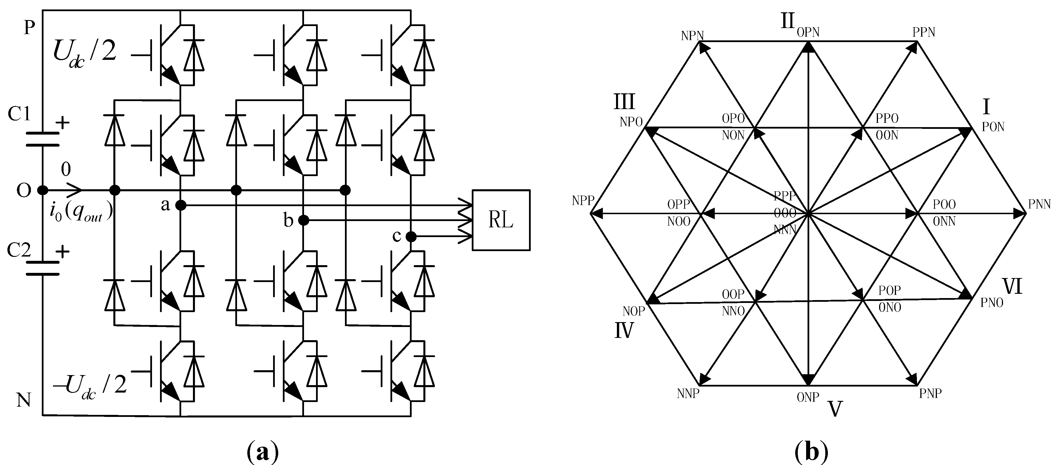
A Varied VSVM Strategy for Balancing the Neutral-Point Voltage of DC-Link Capacitors in Three-Level NPC Converters

State Key Laboratory of Advanced Electromagnetic Engineering and Technology, Huazhong University of Science and Technology, Wuhan 430074, China
*
Author to whom correspondence should be addressed.
Energies 2015, 8(3), 2032-2047; https://doi.org/10.3390/en8032032
Submission received: 6 January 2015 / Revised: 18 February 2015 / Accepted: 28 February 2015 / Published: 13 March 2015

Abstract

:
In the research field of multilevel converters, three-level NPC (neutral-point-clamped) converters, which unfortunately may cause the deviation of the neutral-point voltage of DC-link capacitors, are widely discussed. Theoretically, virtual space vector modulation (VSVM) could guarantee the balance control of the neutral-point voltage. However, there still exist some uncontrollable space vector regions. Based on VSVM, this paper proposes a varied virtual space vector modulation (VVSVM) method for three-level NPC converters. Under complete modulation conditions, this method can control the balance of the neutral-point voltage of DC-link capacitors by adjusting the duty cycle of small vectors and regulating the current generated by virtual medium vectors. Compared with commonly used VSVM methods and mixed modulation strategies, this method is simpler and more practical. The effectiveness and validity of this method are verified by simulations and experiments.

1. Introduction

Multilevel converter topologies are considered to be the best choice for medium and high voltage applications for their less output harmonic voltage and higher voltage level. Among the multilevel converter topologies, the three-level neutral-point clamped (NPC) converter, as shown in Figure 1a, is a widely-researched topology [1,2]. Nevertheless, owing to its topology characteristics, the capacitor’s neutral-point voltage sometimes fluctuates when the three-level NPC converter works, and this causes harmonic distortion of the three phase output voltage, which limits its wide use [3,4,5].
Figure 1. Schematic of a three-level NPC converter. (a) Topology structure of three-level NPC converter; (b) Distribution diagram of voltage vectors.
Energies 08 02032 g001
In recent years, the balance control of neutral-point voltage has been a hot topic and some strategies have been proposed in [6,7,8,9]. Among these strategies, space vector modulation (SVM) is one of the most commonly used modulation strategies, which has the advantages of low switching frequency and better output voltage quality [10,11]. However, when SVM is applied, the medium vectors will affect the neutral-point voltage, which will cause low-frequency oscillations in the neutral-point voltage under high modulation conditions [12]. The paper [13] proposed an improved SVM excluding medium vectors. It can solve the low-frequency voltage oscillation issue. However, without the medium vectors to synthesize the space vectors, this will increase the possibility of distortion of the output voltage and increase the harmonic content of the output voltage. The paper [14] proposed a new SVM, which can balance the neutral-point voltage of DC-link capacitors by modulating the conduction time of the switch tube.
Furthermore, the papers [15,16] proposed a VSVM method which has been theoretically proven not to cause oscillation on the neutral-point voltage. This strategy employs an optimized virtual space vector with less distortion of the output voltage. However, the criterion to design the controller for neutral-point balancing is not presented in these papers. In practice, the balance of neutral-point voltage of DC-link capacitors is not very satisfactory, owing to the asymmetric parameters of components, switching delay and asymmetry of DC-link capacitors. Based on VSVM, the paper [17] proposed a method to balance the neutral-point voltage according to the fact that positive and negative small vectors have opposite effects on the neutral-point voltage. Although this method combines the merits of VSVM and SVM, the neutral-point voltage can’t be controlled in some space vector regions when the modulation index m is between 0.667 and 1 (0.667 < m < 1), because there is not a pair of positive and negative small vectors in some vector regions. The papers [18,19,20,21] proposed some mixed strategies switching between the method of VSVM and SVM in some space vector regions, but the above methods are quite complex to manipulate. The paper [22] proposed a method to restrict the fluctuation of the neutral-point voltage of DC-link capacitors by optimizing the switch tube order. Because the three-level NPC converter itself has many vectors, increasing the number of switch sequence choices makes it more complex to programme.
In this paper, a varied virtual space vector modulation (VVSVM) is proposed on the basis of VSVM not affecting the balance of DC-link capacitors voltage theoretically [15], and the proposed strategy is designed to keep the balance of the neutral-point voltage of DC-link capacitors through adjusting the duty cycle of small vectors and regulating the current generated by virtual medium vectors. Unlike the conventional VSVM, when the modulation index is between 0.667 and 1, this strategy can maintain the balance of the neutral-point voltage of DC-link capacitors in all vector regions where the conventional VSVM strategy cannot. Experiment and simulation have verified the effectiveness of the proposed strategy.

2. Varied Virtual Space Vector Modulation

In the typology of a three-level NPC converter, as shown in Figure 1a, P, O and N represent three output voltage values: Udc/2, 0, −Udc/2, where Udc is the DC-link voltage. Figure 1b is the distribution diagram of the voltage vectors, from which we can know that the NPC converter has 27 space vectors. According to the definition and distribution of virtual space vectors in VSVM [15,16], this paper designs a group of new varied virtual space vectors. Taking sextant I as an example, the virtual voltage vectors are established in sextant I, as shown in Figure 2a.
Figure 2. Distribution of varied virtual space voltage vectors in sextant I; (a) Definition and distribution of varied virtual space voltage vectors in sextant I; (b) Virtual space voltage vectors in g_h coordinate; (c) Distribution diagram of varied virtual vectors in Sextant I (60° Sextant); (d) The calculation of m1.
Energies 08 02032 g002aEnergies 08 02032 g002b

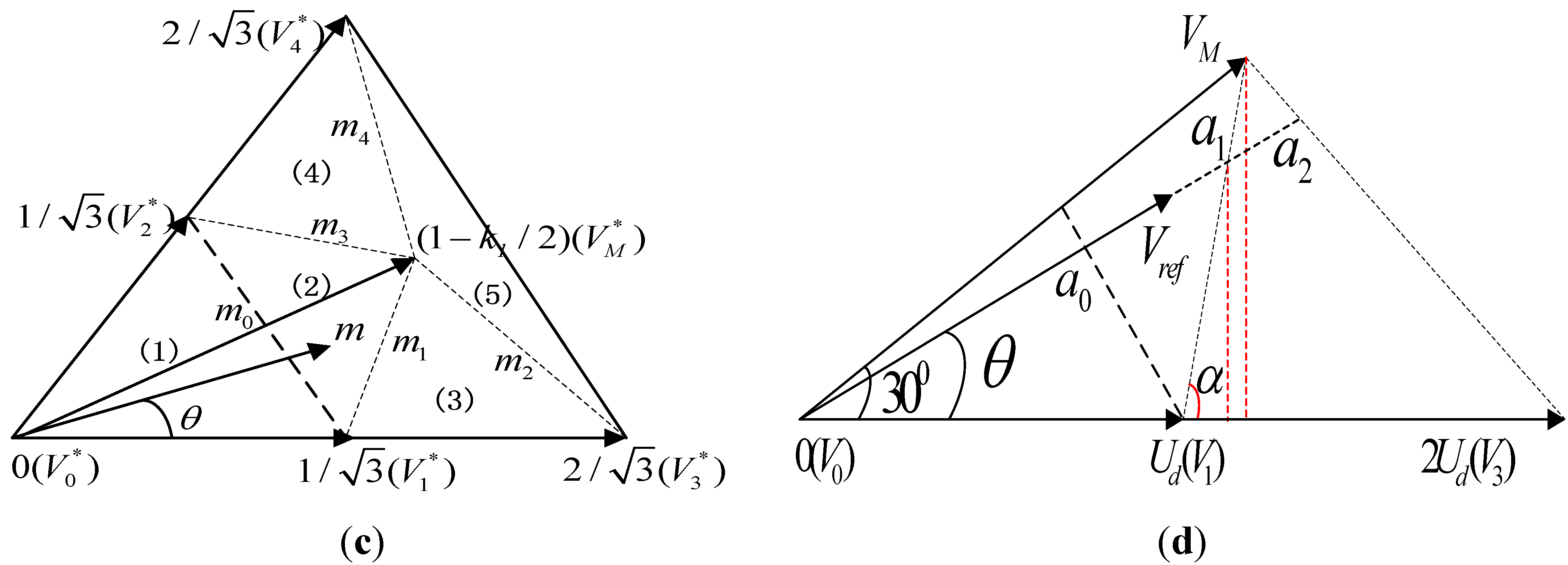
2.1. The Definition of Varied Virtual Space Vectors

(a) Definition of virtual small vectors: the virtual small vectors are built under the precondition that positive and negative small vectors have opposite interactions on the neutral-point voltage fluctuation. Taking the positive and negative small vectors (POO (−ia), ONN (ia)) for example, the virtual small vector (VVS1) is formed as follows (VVS2 is formed in a similar way):
V VS 1 = k V POO + ( 1 k ) V ONN ,    a n d     0 k 1
Assuming that the three phases current (ia, ib, ic) stay unchanged in a short switching period TS, during the duty cycle TVS1 of a virtual small vector VVS1, the three phase load current ia, ib, ic is connected to the neutral-point O, the charge flowing out from which is represented as:
q VS 1 = i a k T VS 1 + i a ( 1 k ) T VS 1
It is noted that when k = 1/2, the charge from the neutral-point O: qVS1 = 0, so during the duty cycle TVS1 of virtual small vector VVS1, the neutral-point voltage of DC-link capacitors is not affected.
(b) Definition of varied virtual medium vectors: assuming that during a switching period TS, the three-phase currents ia, ib, ic stay steady, and ia + ib + ic = 0. By combining the small vectors VPPO (ic) and VONN (ia) and the medium vectors VPON (ib), a virtual medium vector VM is synthesized as follows:
V M = ( k 1 2 V ONN + k 2 V PON + k 1 2 V PPO )
k 1 + k 2 = 1 ,     a n d    k 1 > 0 ,   k 2 > 0
From Equations (3) and (4), it can be seen that during the duty cycle Tm of virtual medium vector VM, the three phase load current will be connected to the neutral-point O respectively at a different time. The charge flowing out from the neutral-point (O) is described as follows, during the duty cycle Tm of the virtual medium vector:
q T m = 0 T S i o d t = 0 T m k 1 2 i a d t + 0 T m k 2 i b d t + 0 T m k 1 2 i c d t = T m ( k 1 2 i a + k 2 i b + k 1 2 i c ) = T m ( 1 3 k 1 2 ) i b
Equation (6) describes the relationship between the voltage of capacitors and the charge flowing out from the neutral-point:
Δ ( U c 1 U c 2 ) = 1 C q T m
During the duty cycle Tm of varied virtual space vector, the following conclusions are drawn according to Equations (5) and (6):
(1)
When k1 = 2/3, the virtual medium vector locates at the point b, and the charge qTm flowing out from the neutral-point O is zero. This virtual medium vector will not cause a fluctuation of the neutral-point voltage, which is the same as the neutral-point voltage in the traditional VSVM (modulation index m = 0.667). Because the length of the virtual medium vector stays steady in the process of synthesizing the voltage space vector Vref, the traditional VSVM can’t use the virtual medium vector to balance the neutral-point voltage of DC-link capacitors.
(2)
When 1 > k1 > 2/3, the virtual medium vector locates between a and b.
  • If ib > 0, the charge flowing out from the neutral-point O: qTm < 0, and UC1 gets smaller; UC2 get larger.
  • If ib < 0, the charge flowing from the neutral-point O: qTm > 0, and UC1 gets larger; UC2 get smaller.
(3)
When 2/3 > k1 > 0, the virtual medium vector locates between b and c.
  • If ib > 0, the charge flowing from the neutral-point O: qTm > 0, and UC1 gets larger; UC2 get smaller.
  • If ib < 0, the charge flowing out from the neutral-point O: qTm < 0, and UC1 gets smaller; UC2 get larger.
(c) Definition of virtual zero vectors: VV0 = VOOO. The virtual zero vectors don’t affect the neutral-point voltage.
(d) Definition of virtual long vectors: VVL1 = VPNN, VVL2 = VPPN. The virtual long vectors don’t affect the neutral-point voltage.

2.2. Judgment of Small Regions in 60° Sextant

As shown in Figure 2a, taking sextant I for example, it can be divided into five small regions (1)–(5), according to the location of vectors (Udc denotes the DC-link voltage, Vref is the reference vector, θ is the reference vector angle, Ud denotes Udc/3 and the modulation index is defined as: m = | V ref | / 3 U d ).
The length of varied virtual medium vector can be represented by Equation (7):
{ | V M | = 3 U d ( 1 k 1 / 2 ) U d = U dc / 3
As shown in Figure 2d, the following formula is derived as:
{ tan α = | V M | / 2 3 | V M | / 2 U d tan α = a 1 sin θ a 1 cos θ U d
where:
m 1 = a 1 / ( 3 U d )
As shown in Figure 2c, from Equations (8) and (9), the m1 is written as:
m 1 = | V M | 3 ( sin θ ( 2 U d 3 | V M | ) + | V M | cos θ )
Similarly, the calculation formulas of m0, m1, m2, m3, m4 are expressed as follows:
{ m 0 = 1 / ( 3 cos θ + sin θ ) m 1 = | V M | 3 ( sin θ ( 2 U d 3 | V M | ) + | V M | cos θ ) m 2 = 2 | V M | 3 ( sin θ ( 4 U d 3 | V M | ) + | V M | cos θ ) m 3 = | V M | 3 ( sin ( 60 0 θ ) ( 2 U d 3 | V M | ) + | V M | cos ( 60 0 θ ) ) m 4 = 2 | V M | 3 ( sin ( 60 0 θ ) ( 4 U d 3 | V M | ) + | V M | cos ( 60 0 θ ) )
The small region in which the reference vector locates is confirmed according to Equations (7) and (11), the modulation index and the regulation of judging small region (Table 1).
Table 1. Judging the small region of the reference vector.
Small regionCondition 1Condition 2
(1) 0 < m m 0 -
(2) m 0 < m m 1 0 θ < π / 6
m 0 < m m 3 π / 6 θ < π / 3
(3) m 1 < m m 2 0 θ < π / 6
(4) m 3 < m m 4 π / 6 θ < π / 3
(5)Other-

2.3. Synthesis of Vectors

From the divided small regions in sextant I above, three virtual voltage vectors are determined to synthesize the reference vector. To simplify the calculation, we choose 60° coordinate (g_h coordinate) to calculate the time of vector synthesis. Taking the space voltage vector Vref which locates at region (2) for example, the duty cycle of the relative vectors is calculated as follows.
As shown in Figure 2b, in the g_h coordinate, the reference voltage vector Vref can be represented as:
{ V g = V ref ( cos θ sin θ / 3 ) V h = 2 V ref sin θ / 3
According to the principle of vectors synthesis, the modulation rules of the nearest three vectors are established as follows:
{ T s V g = U d T 1 + X T m T s V h = U d T 2 + X T m                 T s = T 1 + T 2 + T m
where (X = Ud(1 − k1/2) represents the projection of virtual medium vector on the g-axis and h-axis.)
From Equations (12) and (13), we obtain the following equation:
{ T 1 = T s [ V h X + V g ( U d X ) U d X ] U d ( U d 2 X ) T 2 = T s [ V g X + V h ( U d X ) U d X ] U d ( U d 2 X ) T m = T s T 1 T 2
Similarly, the duty cycle of other virtual vectors is calculated, and Table 2 shows the duty cycle of virtual vectors in sextant I.
Table 2. Duty cycle of voltage vectors in sextant I.
Small regionDuty cycle 1Duty cycle 2Duty cycle 3
region ( 1 ) V 0 , V 1 , V 2 T 1 = T s V g U d T 2 = T s V h U d T 0 = T s T 1 T 2
region ( 2 ) V 1 , V 2 , V M 1 T 1 = T s [ V h X + V g ( U d X ) U d X ] U d ( U d 2 X ) T 2 = T s [ V g X + V h ( U d X ) U d X ] U d ( U d 2 X ) T m = T s T 1 T 2
region ( 3 ) V 1 , V 3 , V M 1 T 3 = T s [ V g X + V h ( U d X ) U d X ] U d X T m = T s V h X T 1 = T s T 3 T m
region ( 4 ) V 2 , V 4 , V M 1 T 4 = T s [ V h X + V g ( U d X ) U d X ] U d X T m = T s V g X T 2 = T s T 4 T m
region ( 5 ) V 3 , V 4 , V M 1 T 3 = T s [ V g ( 2 U d X ) + V h X 2 U d X ] 4 U d ( U d X ) T 4 = T s [ V h ( 2 U d X ) + V g X 2 U d X ] 4 U d ( U d X ) T m = T s T 3 T 4

2.4. The Amplitude of the NP Voltage Oscillations

In a switching period, the NP voltage ripple of the NPC converter is defined as:
Δ u 1 = I ave T m C
where Δ u 1 is the amplitude of the ripple on the neutral-point voltage, I ave is the average neutral-point current, T m is the duty cycle of the virtual medium vector, C is the value of the DC-link capacitors. Thus, increasing the value of the capacitors and the switching frequency is helpful for balancing the neutral-point voltage.

3. Neutral-Point Balancing Strategy

3.1. Neutral-Point Balancing Algorithm in Small Region (1)

Taking sextant I for example, we choose the small vectors to synthesize the reference vector when reference vector Vref locates in small region (1) in this paper. Assuming that the three phase output currents (ia, ib, ic) stay constant in a switching period TS, where dmin symbolizes the duty cycle of virtual small vector (V1), dmin_p and dmin_n respectively represents the duty cycle of the positive small vector (VPOO) and negative small vector (VONN), and dmin_p + dmin_n = dmin; imin_p(−ia) represents the neutral-point current of dc-link capacitors during the duty cycle of positive small vector; imin_n(ia) represents the neutral-point current of DC-link capacitors during the duty cycle of negative small vector. As shown in Figure 1a, the charge qout flowing out of the neutral-point O over a switching period TS can be represented as follows:
q o u t = i min _ p d min _ p + i min _ n d min _ n = i min _ p k d min + i min _ p ( k 1 ) d min = ( 2 k 1 ) i min _ p d min ,       a n d     ( 0 k 1 )
During the switching period TS, the relationship between the capacitors voltage and the charge flowing out of the neutral-point O can be represented as:
Δ ( U c 1 U c 2 ) = 1 C q out
From Equations (16) and (17), we can obtain the following equation:
Δ ( U c 1 U c 2 ) = 1 C ( 2 k 1 ) d min i min _ p
If the voltage transducer detects the deviation (ΔU) of neutral-point voltage, then during the next switching period the current of the positive and negative small vectors should generate voltage –ΔU to offset the deviation, and keep the balance of the neutral-point voltage of DC-link capacitors. Therefore, according to Equation (18), we could calculate the value of control factor k in the next sampling period.

3.2. Balancing Strategy for Neutral-Point Voltage in Small Regions (2)–(5)

The neutral-point current generated by the virtual medium vector is used to offset the voltage deviation of DC-link capacitors, which can realize the voltage balance in the small regions (2)–(5). As a result, the balance of neutral-point voltage can be maintained in VVSVM, when the modulation index is between 0 and 1 (0 < m < 1).
Taking sextant I for example, the location of virtual medium vector could be determined by detecting the fluctuation of neutral-point voltage in the next sampling period to maintain the balance of the neutral-point voltage. During the duty cycle of virtual medium vector, the following equation is obtained according to Equations (5) and (6):
{ Δ ( U c 1 U c 2 ) = 1 C T m ( 1 3 k 1 2 ) i b     ( 0 < k 1 < 1 )
If the reference vector voltage Vref locates between small region (2) to (5) and the deviation ΔU of the neutral-point voltage is detected, the virtual medium vector current could generate −ΔU voltage to offset the deviation during the next switching period TS. According to Equation (19), the fluctuation of neutral-point voltage of DC-link capacitors can only judge whether the virtual medium vector locates at a-b or b-c as shown in Figure 2a. Because the neutral-point voltage doesn’t change a lot in a sampling period, this paper uses Tm' of the previous sampling period to calculate the approximate value of k1.

4. Simulation and Experimental Verification

This section presents the simulation and experiment results of three level neutral-point NPC converter to verify the effectiveness of the proposed VVSVM strategy by comparing it with the VSVM strategy. Simulation and experiment environments are performed as follows: DC-link voltage: Udc = 400 V; three-phase resistance-inductance load: R = 15 Ω, L = 10 mH; DC-link capacitors: C1 = C2 = 2000 μF; sampling frequency: 8 kHz; fundamental frequency: 50 Hz. The dead time of the system is set as 3 μs and the modulation index is 0.83.

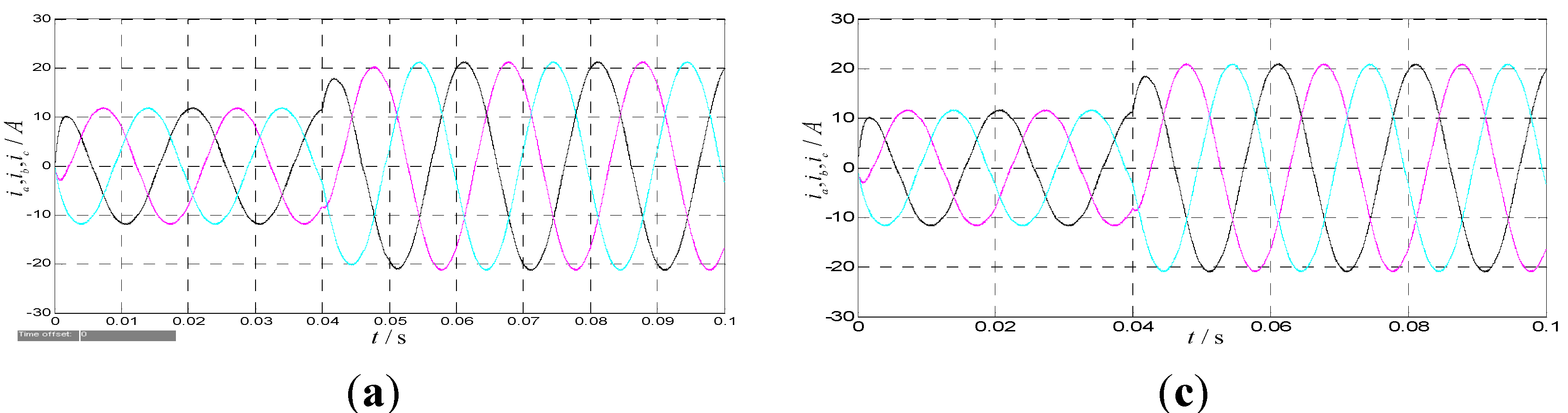
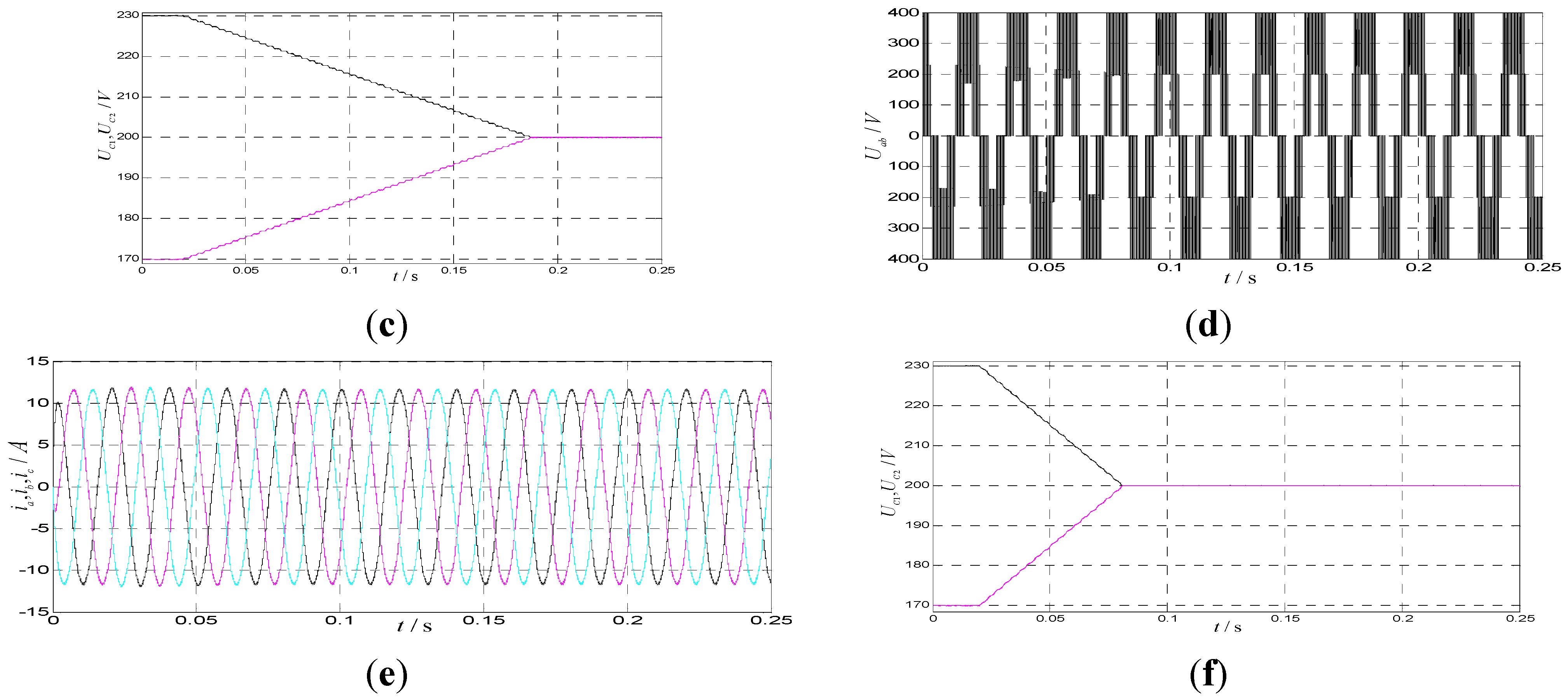
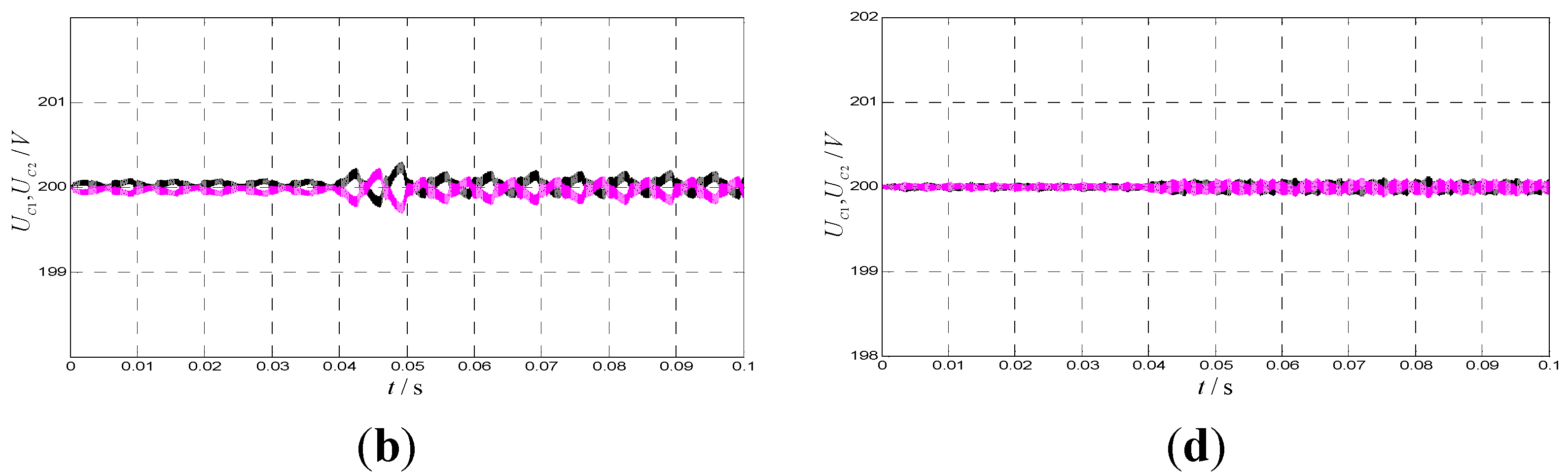
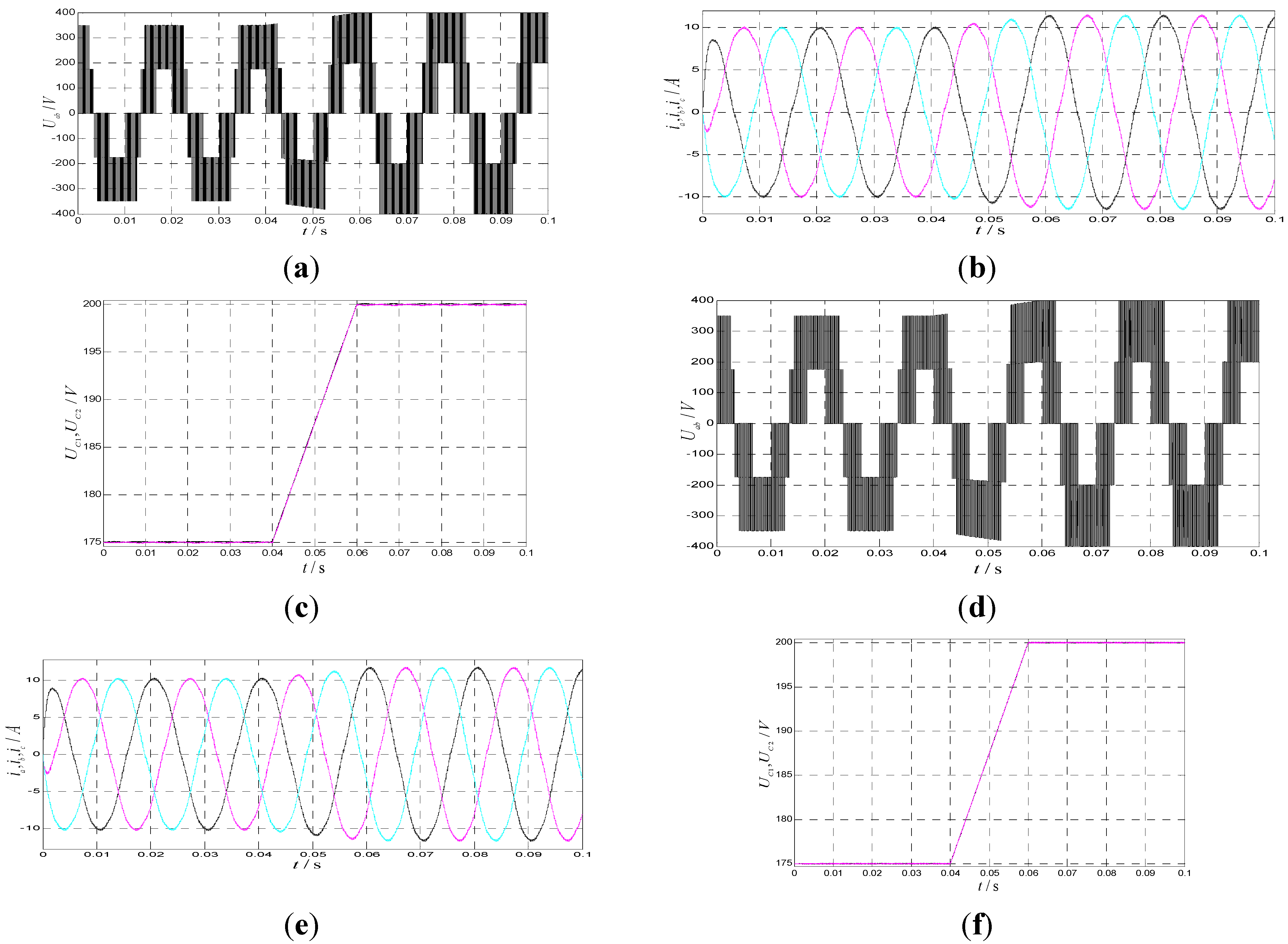
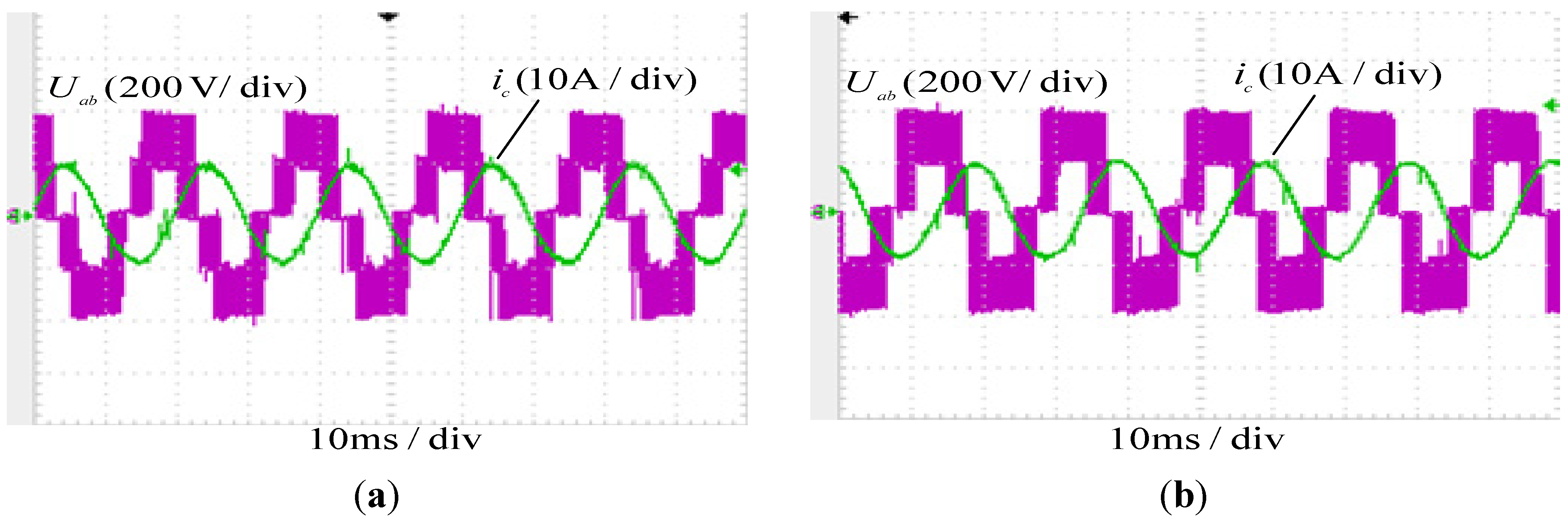
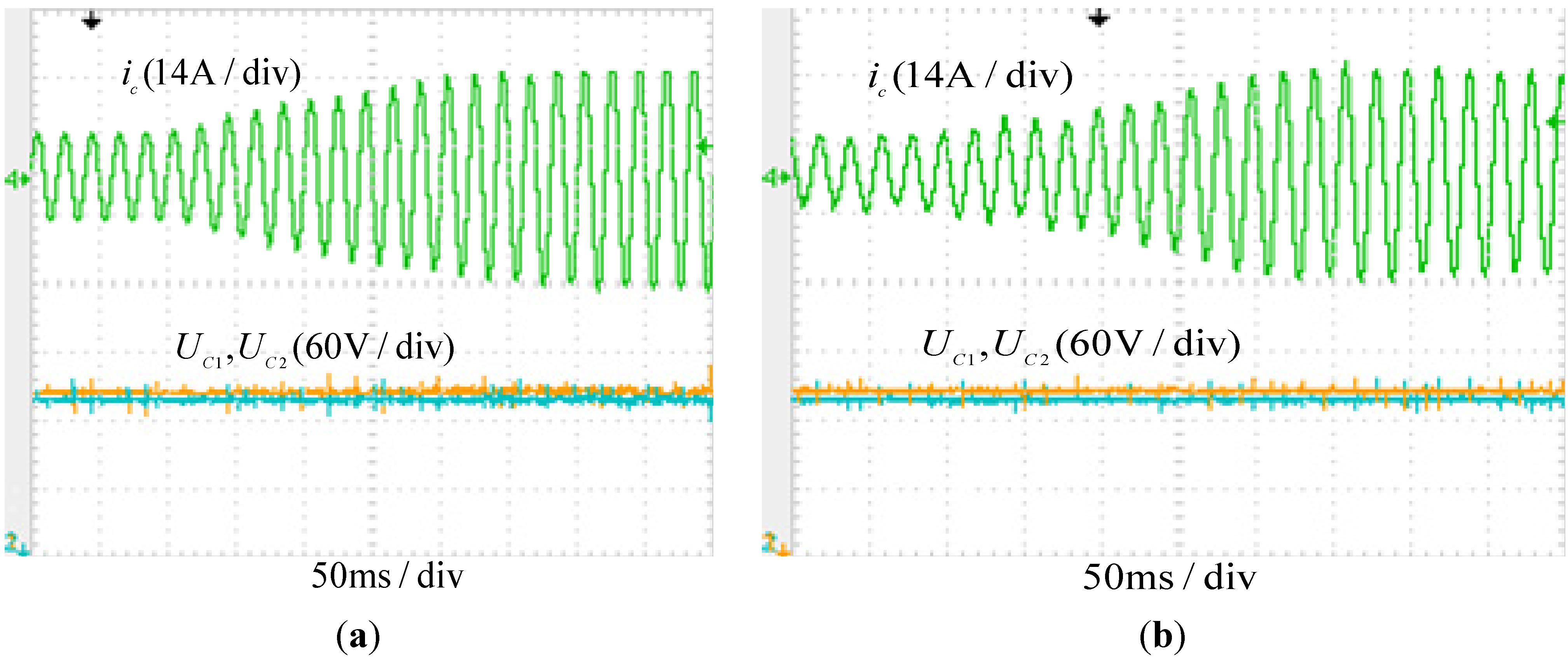
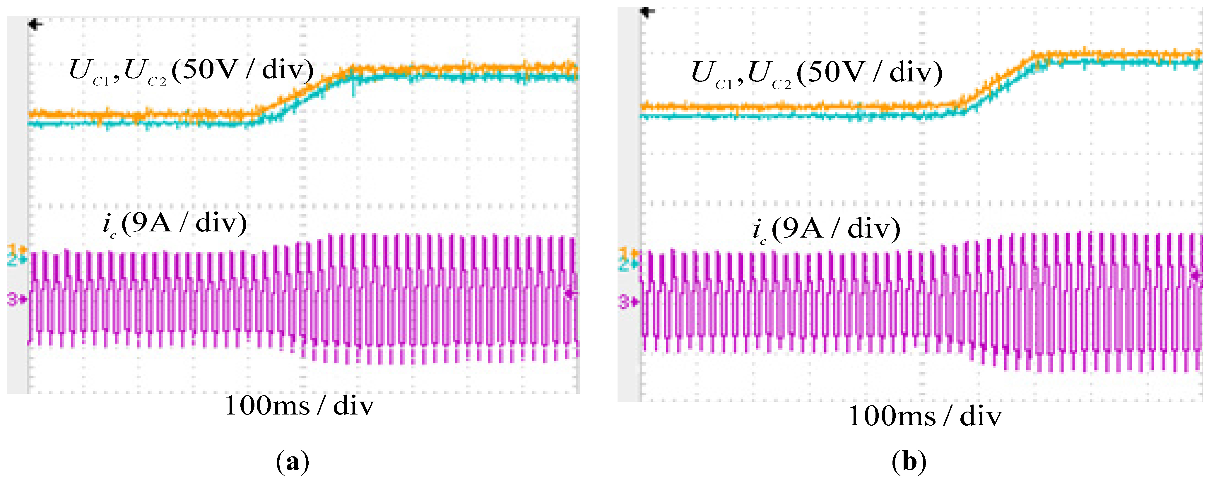
4.1. Simulation Results

To verify the balancing performance of the proposed modulation technique, the initial voltage of the DC-link capacitors is set as: UC1 = 230 V, UC2 = 170 V. In the simulation process, from 0 s to 0.02 s, the deviation of capacitors voltage is maintained at 60 V by VSVM and VVSVM, and after 0.02 s the deviation of capacitors voltage is controlled to be zero.
Figure 3a–c shows the simulation results of VSVM which uses small vectors to balance the neutral-point voltage. Figure 3d–f shows the simulation results of the proposed VVSVM. By comparison of Figure 3c,f, either the VSVM or VVSVM can balance the capacitors voltage, but the dynamic balancing process of the capacitors voltage in VVSVM is faster than that of the capacitors voltage in VSVM.
When the modulation index is 1 > m > 0.667 in VSVM strategy, the tip of reference vector (Vref) is bound to fall in the region (5) of sextants I–VI because there is no pair of positive and negative small vectors for synthesizing Vref in the small region (5). Thus, the VSVM strategy can’t balance the deviation of capacitors voltage in this region. However, in the region (5), the proposed VVSVM strategy can control the balance of neutral-point voltage by regulating the current of the virtual medium vectors in region (5). So the balancing adjustment time of VVSVM is less than that of VSVM. From Figure 3a,d, it can be seen that line-line voltage waveform varies responding to the capacitors voltage varying through using VSVM and VVSVM.
Figure 3. Simulation results of balancing DC-link capacitors voltage; (a) balancing process of line-to-line voltage in VSVM; (b) three phase currents in VSVM; (c) balancing process of DC-link capacitors voltage in VSVM; (d) balancing process of line-to-line voltage in VVSVM; (e) three phase currents in VVSVM; (f) balancing process of DC-link capacitors voltage in VVSVM.
Energies 08 02032 g003aEnergies 08 02032 g003b
Figure 4a,b shows the simulation results of VSVM under the condition of varying load. Figure 4c,d shows the simulation results of VVSVM under the condition of varying load. The voltage of DC-link capacitors is initially set as UC1 = 200 V, UC2 = 200 V. The load resistance suddenly changes from 15 to 8 Ω at 0.02 s. It can be seen that the load currents vary from 12 to 21 A at 0.04 s. Comparing Figure 4b,d, it can be seen that the voltage of the DC-link capacitors barely changes responding to changing the load, using the VVSVM. However, in VSVM strategy the DC-link capacitors voltage fluctuates obviously. Figure 5 shows the simulation results of VSVM and VVSVM in the case of varying DC-link voltage. The DC-link capacitors voltage is initially set as UC1 = 175 V, UC2 = 175 V. The DC-link voltage increased from 350 to 400 V at 0.04 s. Owing to the currents amplitude varying little along with transformed DC-link voltage, it can be seen from Figure 5c,f that the balancing effectiveness of VVSVM is the same as that of VSVM from the simulation results. However, it can be concluded that the VVSVM can better control the voltage balancing of the DC-link capacitors under varying DC-link voltage conditions.
Figure 4. Simulation results of varying load. (a) response of the currents to varying load in VSVM; (b) capacitors voltage during varying load in VSVM; (c) response of the currents to varying load in VVSVM; (d) capacitors voltage during varying load in VVSVM.
Energies 08 02032 g004aEnergies 08 02032 g004b
Figure 5. Simulation results of varying DC-link capacitors voltage; (a) varying process of line-to-line voltage in VSVM; (b) three phase currents in VSVM; (c) varying process of DC-link capacitors voltage in VSVM; (d) varying process of line-to-line voltage in VVSVM; (e) three phase currents in VVSVM; (f) varying process of DC-link capacitors voltage in VVSVM.
Energies 08 02032 g005

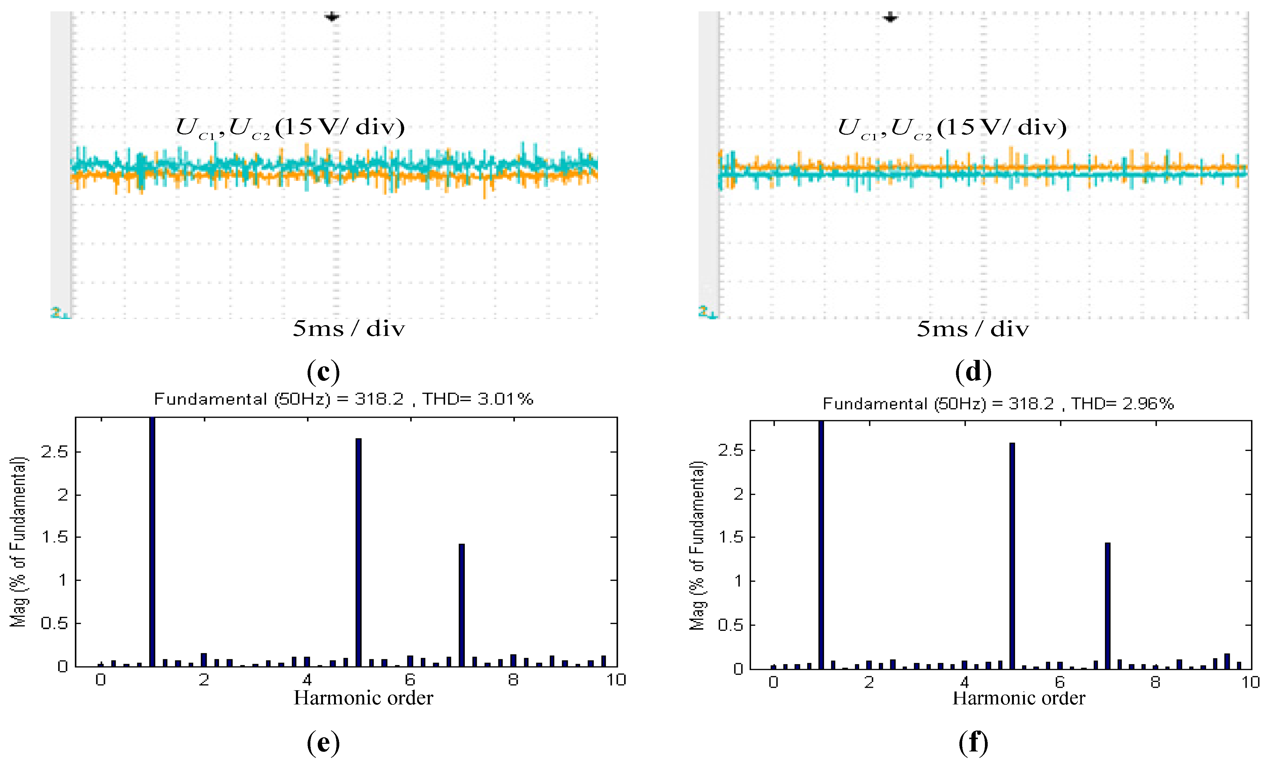
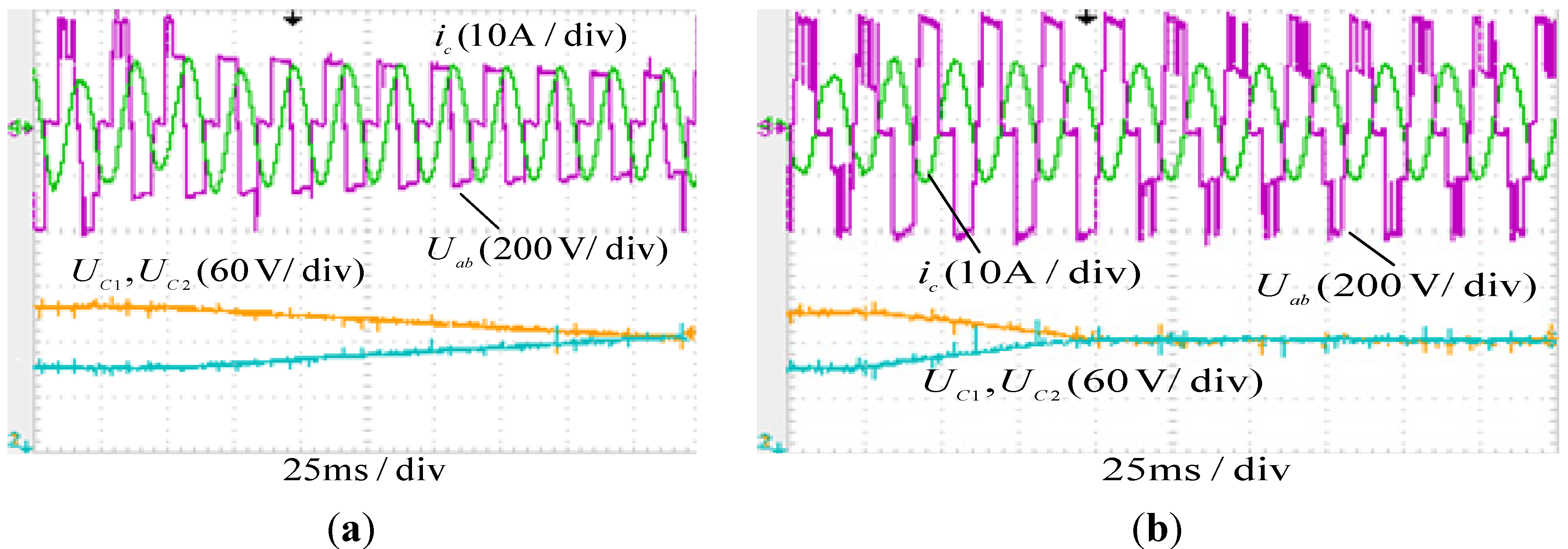
4.2. Experiment Results

To verify the effectiveness of the proposed VVSVM, three-level converter is made of six IGBT (Insulated Gate Bipolar Transistor) dual-modules 2MBI100U4H-170. The main processor is implemented with TMS320F28335 DSP (Digital Signal Processor) controller and EP3C10E144C8 FPGA (Field Programmable Gate Array) is used to generate and output pulse width modulation (PWM) signals for the converter.
Figure 6a,b shows the dynamic balancing of the DC-link capacitors voltage in VSVM and VVSVM, respectively. The voltage deviation is kept at a set value by subtracting a deviation value from the voltage difference of the DC-link capacitors, so the initial deviation between UC1 and UC2 can be controlled. In the initial conditions, the deviation of UC1 and UC2 is keep at 60 V, and then controlled to be 0 V. From Figure 6a,b, it can be seen that the balancing time of the proposed VVSVM is half of that of VSVM, which is significant to the application of the high power and large current. Thus it could be concluded that the proposed VVSVM has a good effectiveness of balancing the capacitors voltage.
Figure 6. Experiment results of balancing the capacitors voltage: (a) VSVM; (b) VVSVM.
Energies 08 02032 g006
Figure 7 shows the balanced state waveforms of the line-to-line voltage and the DC-link capacitors voltage using VSVM and VVSVM. From Figure 7b, it can be seen that when conducting the proposed VVSVM, the line-to-line voltage is a steady three-level wave, that’s to say, UC1 and UC2 stay steady.
Figure 7. Experimental results of VSVM and VVSVM; (a) the line to line voltage and the load current in VSVM; (b) the line to line voltage and the load current in VVSVM; (c) balanced steady state of UC1 and UC2 in VSVM; (d) balanced steady state of UC1 and UC2 in VVSVM; (e) FFT (Fast Fourier Transformation) analysis of line-to-line voltage in VSVM; (f) FFT analysis of line-to-line voltage in VVSVM.
Energies 08 02032 g007aEnergies 08 02032 g007b
Comparing Figure 7c,d, the ripple amplitude of the capacitors voltage in VVSVM is smaller than that in VSVM. The FFT (Fast Fourier Transformation) analysis of the output line-to-line voltage with VSVM and VVSVM is illustrated in Figure 7e,f. THD of the VSVM is about 3.01% and the THD of VVSVM decreases to 2.96%. The 5th and 7th harmonics are included in three level wave of the line to line voltage in VSVM and VVSVM. Figure 8a,b shows the transient behavior of VSVM and VVSVM respectively, when the load varies abruptly. An asynchronous motor is used to verify the effectiveness of the proposed VVSVM in the case of varying load. A step change in the load is done, the asynchronous motor current varies from 7 to 20 A as shown in Figure 8. Since the asynchronous motor current can’t vary abruptly in a very short time, thus, from Figure 8a,b, the balancing performance of the proposed VVSVM seems to be the same as that of VSVM. However, from the experimental results, the proposed VVSVM has better effectiveness of balancing voltage of DC-link capacitors compared to VSVM. It can be concluded that the capacitors voltage ripple is suppressed satisfactorily under the case of varying load when employing VVSVM.
Figure 8. Experimental results of varying load. (a) VSVM; (b) VVSVM.
Energies 08 02032 g008
Figure 9a,b shows the experimental results of VSVM and VVSVM when the DC-link voltage is changed from 300 to 400 V. The figures show that the load current varies responding to changing DC-link voltage. From the analysis above, the neutral-point current flowing in/out of the capacitors is the only reason causing the capacitors’ voltage unbalance, so the difference of balancing effectiveness in both VSVM and VVSVM is not very obvious in the case of varying DC-link voltage. However, from the experimental results, it can be seen that the proposed VVSVM is also able to maintain the neutral-point voltage balance in this case.
Figure 9. Experimental results of varying DC-link voltage. (a) VSVM; (b) VVSVM.
Energies 08 02032 g009

5. Conclusions

This paper proposed a VVSVM strategy for balancing the neutral-point voltage through adjusting the duty cycle of small vectors and regulating the current generated by virtual medium vectors. In the case of higher modulation index (m > 0.667), compared with VSVM which can’t balance the neutral-point voltage in some vector regions (small region (5) in the paper), the proposed VVSVM can perfectly keep the balance of neutral-point voltage in all the vector regions. Simulation and experiment show that when employing VVSVM, the balance of neutral-point voltage can be effectively maintained with less distortion of the output voltage, thus providing an effective strategy for high voltage applications.

Acknowledgments

The authors gratefully acknowledge Shanming Wan and Fang Wu for their work on the hardware setup. This project is supported by the National Natural Science Foundation of China under Grants 51377064 and 51407080.

Author Contributions

Shi Weng Gui conducted the theory analysis and the simulation. Shi Weng Gui and Zhen Jun Lin performed the experimental test, and Sheng Hua Huang designed the whole project and edited the manuscript.

Conflicts of Interest

The authors declare no conflict of interest.

References

  1. Rodriguez, J.; Bernet, S.; Bin, W.; Pontt, J.O.; Kour, S. Multilevel voltage source converter for industrial medium voltage drives. IEEE Trans. Ind. Electron. 2007, 54, 2930–2945. [Google Scholar] [CrossRef]
  2. Chaves, M.; Margato, E.; Silva, J.F.; Pinto, S.F. New approach in back-to-back m-level diode-clamped multilevel converter modeling and direct current bus voltages balancing. IEEE Trans. Power Electron. 2010, 3, 578–589. [Google Scholar] [CrossRef]
  3. Nabae, A.; Takahashi, I.; Akagi, H. A new neutral-point clamped PWM inverter. IEEE Trans. Ind. Appl. 1981, 5, 518–523. [Google Scholar] [CrossRef]
  4. Rodriguez, J.; Bernet, S.; Steimer, P.K.; Lizama, I.E. A survey on neutral-point-clamped inverter. IEEE Trans. Ind. Electron. 2010, 57, 2219–2230. [Google Scholar] [CrossRef]
  5. Ke, M.; Frede, B. The impact of power switching devices on the thermal performance of a 10 MW wind power NPC converter. Energies 2012, 5, 2559–2577. [Google Scholar] [CrossRef]
  6. Bendre, A.; Venkataramanan, G.; Rosene, D.; Srinivasan, V. Modeling and design of a neutral-point voltage regulator for a three-level diode-clamped inverter using multiple-carrier modulation. IEEE Trans. Ind. Electron. 2006, 53, 718–726. [Google Scholar] [CrossRef]
  7. Pou, J.; Zaragoza, J.; Ceballos, S.; Saeedifard, M.; Boroyevich, D. A carrier-based PWM strategy with zero-sequence voltage injection for a three-level neutral-point-clamped converter. IEEE Trans. Power Electron. 2012, 27, 642–651. [Google Scholar] [CrossRef]
  8. Seo, J.H.; Choi, C.H.; Hyun, D.S. A new simplified space-vector PWM method for three-level inverters. IEEE Trans. Power Electron. 2001, 16, 545–550. [Google Scholar]
  9. Chaturvedi, P.K.; Jain, S.; Agarwal, P. Reduced switching loss pulse width modulation technique for three-level diode clamped inverter technique for three-level diode clamped inverter. IET Power Electron. 2011, 4, 393–399. [Google Scholar] [CrossRef]
  10. Beig, A.R.; Narayanan, G.; Ranganathan, V.T. Modified SVPWM algorithm for three level VSI with synchronized and symmetrical waveforms. IEEE Trans. Ind. Electron. 2007, 54, 486–494. [Google Scholar] [CrossRef]
  11. Zhang, H.; Finney, S.J.; Massoud, A.; Williams, B.W. An SVM algorithm to balance the capacitor voltages of the three-level NPC active power filter. IEEE Trans. Power Electron. 2008, 23, 2694–2702. [Google Scholar] [CrossRef]
  12. Pou, J.; Pindado, R.; Boroyevich, D.; Rodriguez, P. Evaluation of the low frequency neutral-point voltage oscillation in three-level inverter. IEEE Trans. Ind. Appl. 2005, 52, 1582–1588. [Google Scholar]
  13. Grigoletto, F.B.; Pinheiro, H. A space vector PWM modulation scheme for back-to-back three-level diode-clamped converters. In Proceedings of the Power Electronics Conference, 2009, COBEP'09, Bonito-Mato Grosso do Sul, Brazil, 27 September–1 October 2009; pp. 1058–1065.
  14. Choi, U.-M.; Lee, K.B. Space vector modulation strategy for neutral-point voltage balancing in three-level inverter systems. IET Power Electron. 2013, 6, 1390–1398. [Google Scholar] [CrossRef]
  15. Busquets-Monge, S.; Bordonau, J.; Boroyevich, D.; Somavilla, S. The nearest three virtual space vector PWM—A modulation for the comprehensive neutral-point balancing in the three-level NPC inverter. IEEE Power Electron. Lett. 2004, 2, 11–15. [Google Scholar] [CrossRef]
  16. Busquets-Monge, S.; Somavilla, S.; Bordonau, J.; Boroyevich, D. Capacitor voltage balance for the neutral-point-clamped converter using the virtual space vector concept with optimized spectral performance. IEEE Power Electron. Lett. 2007, 22, 1128–1135. [Google Scholar] [CrossRef]
  17. Hu, C.; Wang, Q.; Li, G.; Feng, J.; Jiang, W. A neutral-point potential balancing algorithm for three-level inverter based on virtual-space-vector. Trans. China Electrotech. Soc. 2009, 24, 100–107. [Google Scholar]
  18. Xia, C.; Shao, H.; Zhang, Y.; He, X. Adjustable proportional hybrid SVPWM strategy for neutral-point-clamped three-Level inverters. IEEE Trans. Ind. Electron. 2013, 60, 4234–4241. [Google Scholar] [CrossRef]
  19. Zhang, Y.; Zhao, Z.; Zhu, J. A hybrid PWM applied to high-power three-level inverter-fed induction-motor drives. IEEE Trans. Ind. Electron. 2011, 58, 3409–3420. [Google Scholar] [CrossRef]
  20. Jiang, W.D.; Du, S.W.; Chang, L.C.; Zhang, Y.; Zha, Q. Hybrid PWM strategy of SVPWM and VSVPWM for NPC three-level voltage-source inverter. IEEE Trans. Power Electron. 2010, 25, 2607–2619. [Google Scholar] [CrossRef]
  21. Govindaraju, C. Efficient sequential switching hybrid modulation techniques for multiphase multilevel inverters. IET Power Electron. 2011, 4, 557–569. [Google Scholar] [CrossRef]
  22. Das, S.; Narayanan, G. Novel switching sequences for a space-vector-modulated three-level inverter. IEEE Trans. Ind. Electron. 2012, 59, 1477–1487. [Google Scholar] [CrossRef]

