
A Reflex Charger with ZVS and Non-Dissipative Cells for Photovoltaic Energy Conversion

Abstract
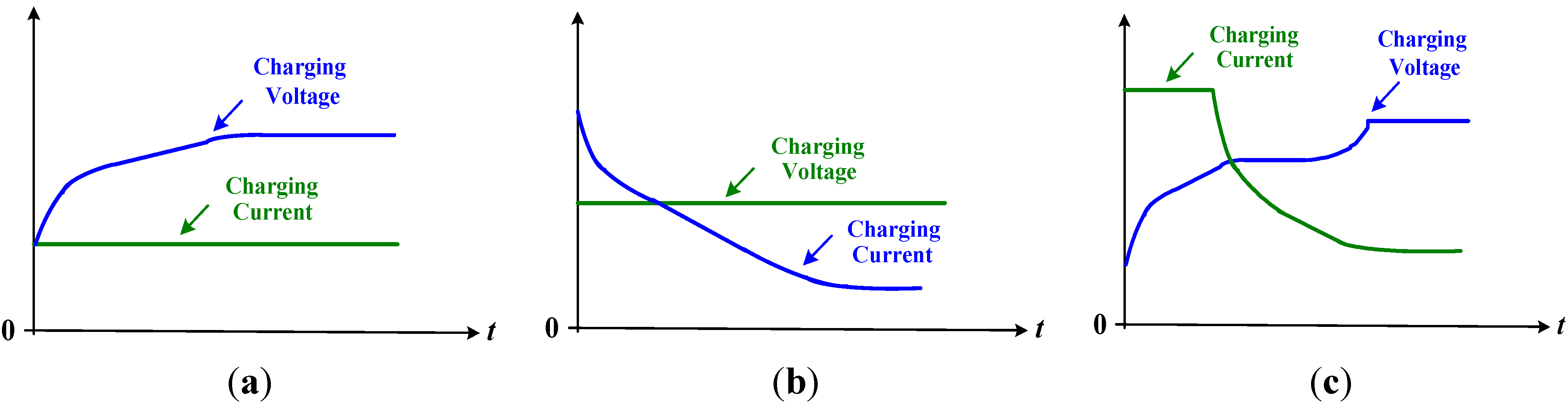
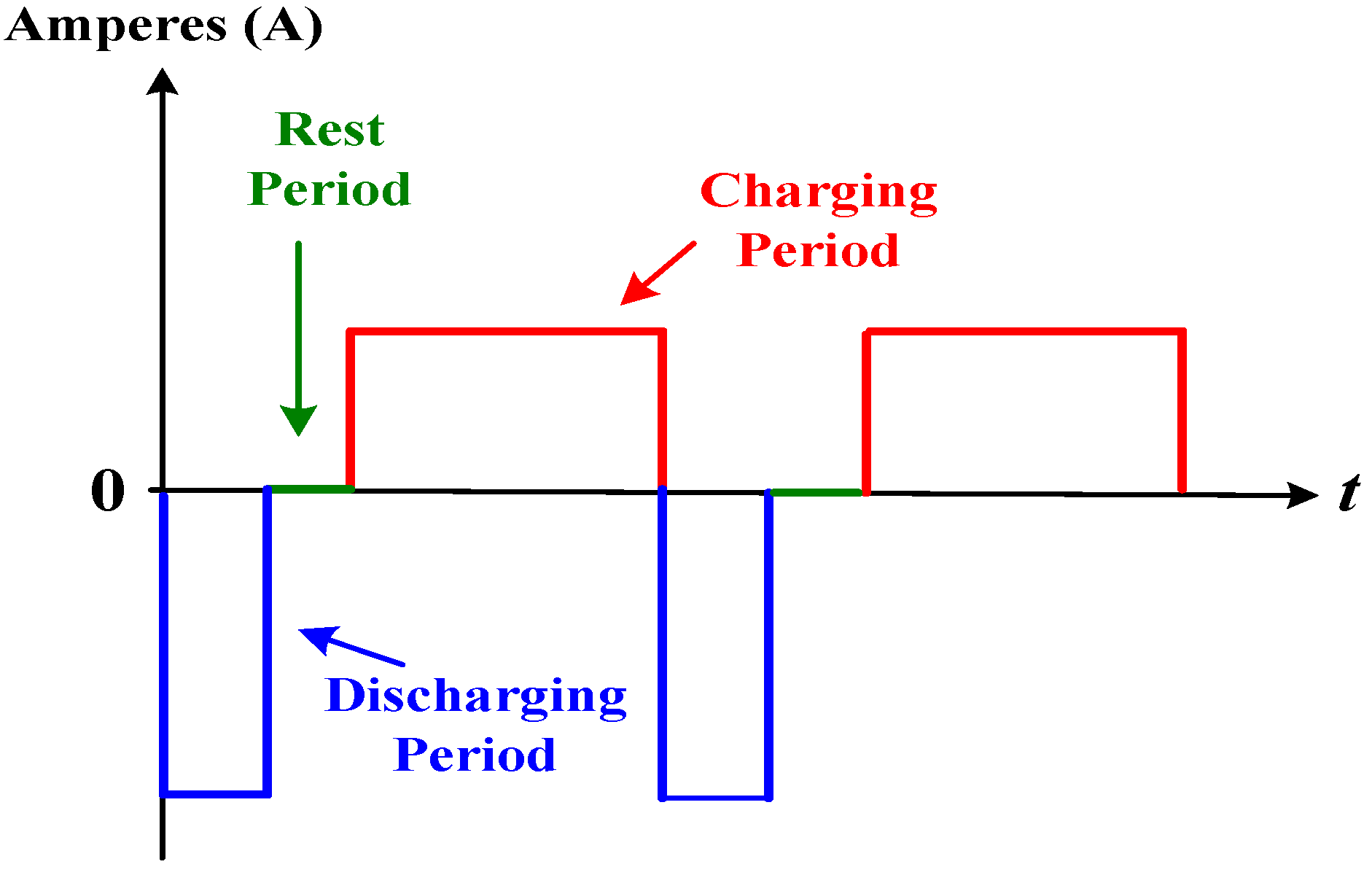
:1. Introduction


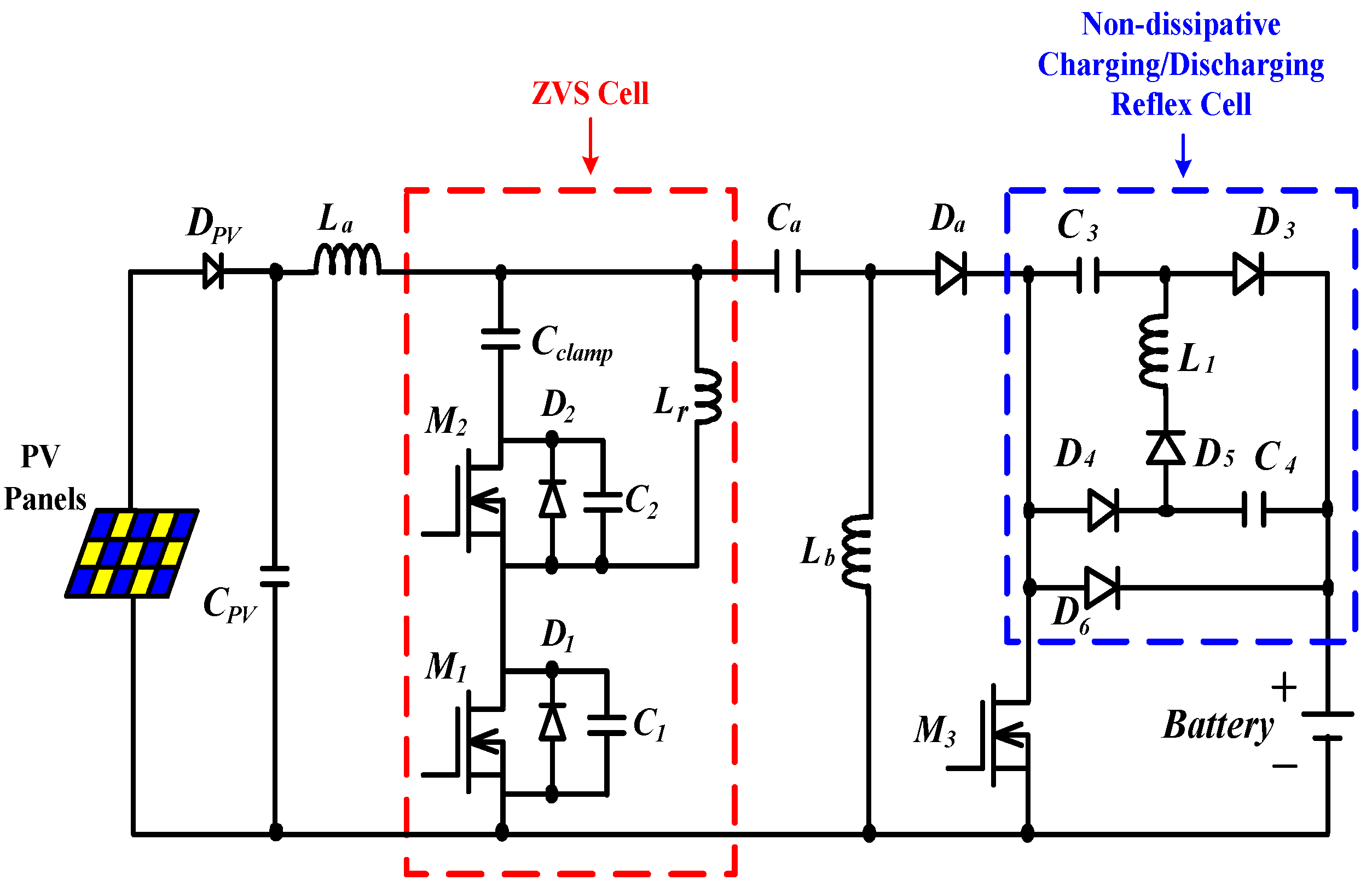
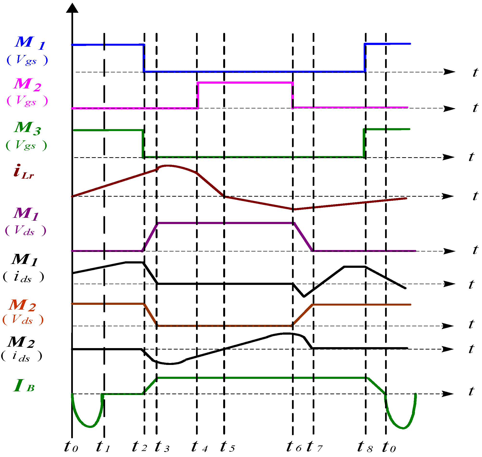
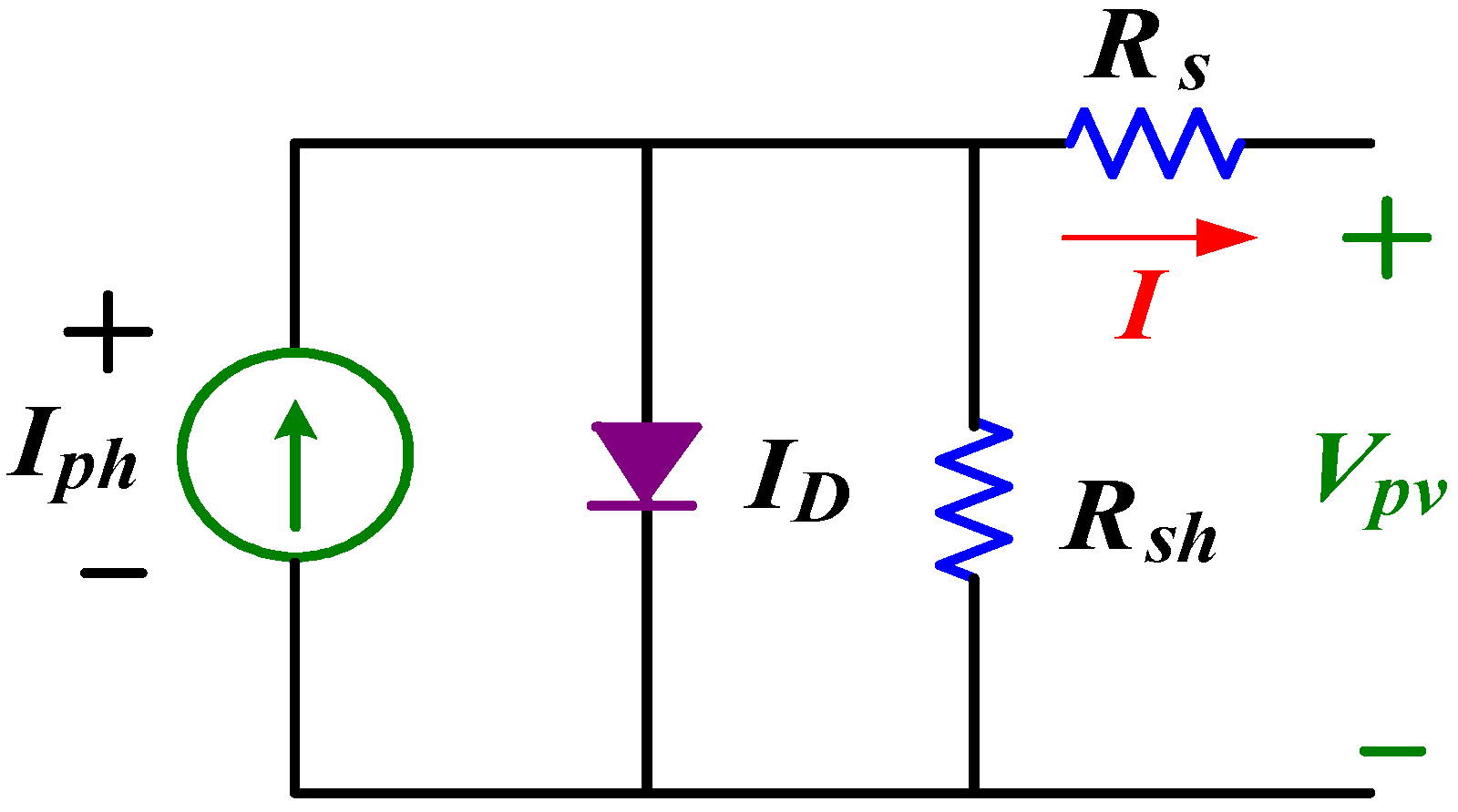
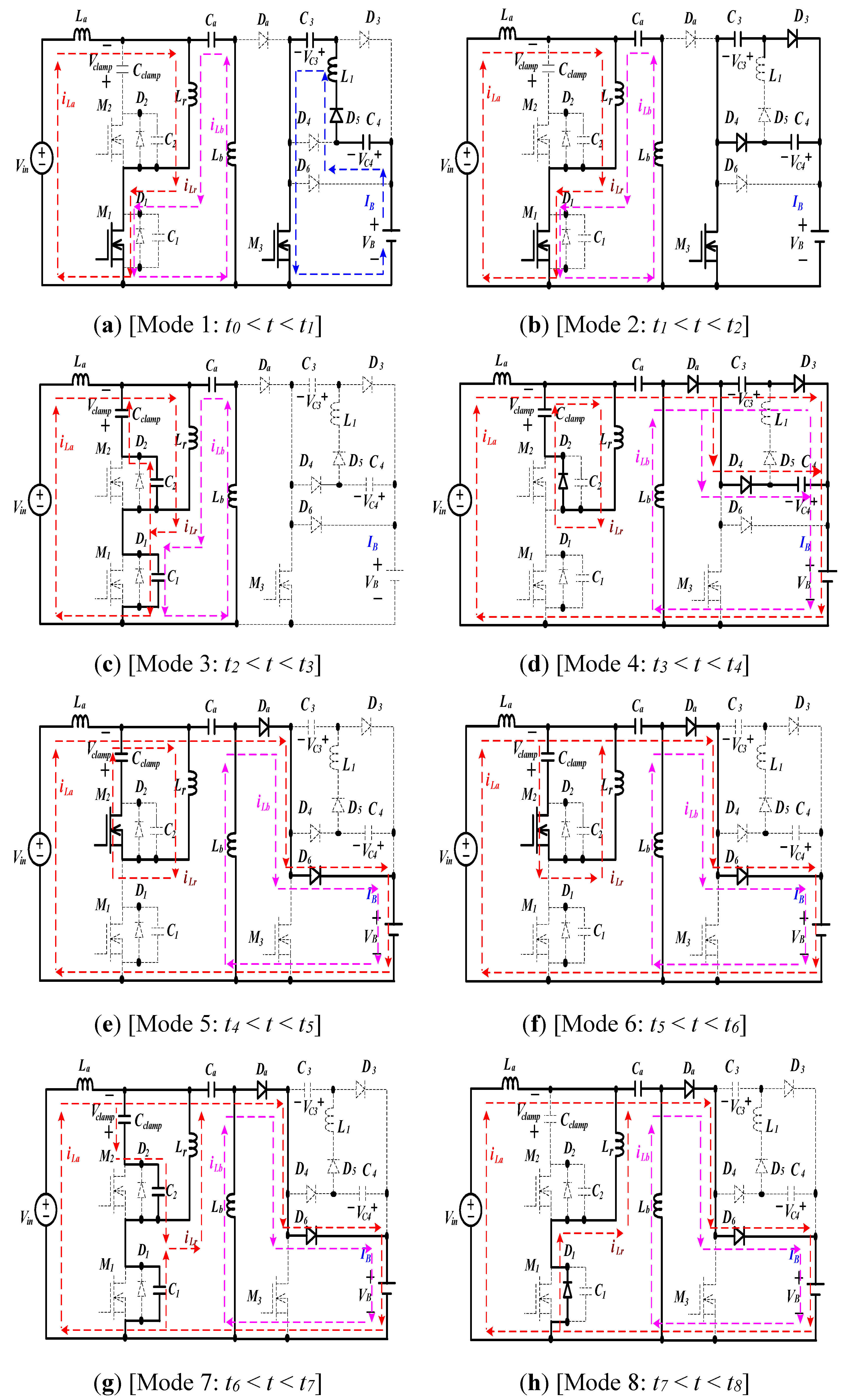
2. Operational Principles

- (1)
- To analyze the ZVS feature, the body diodes (D1 and D2) and parasitic capacitors (C1 and C2) of the active switches (M1 and M2) will be considered at the steady-state operation of the circuit.
- (2)
- All of components are ideal.
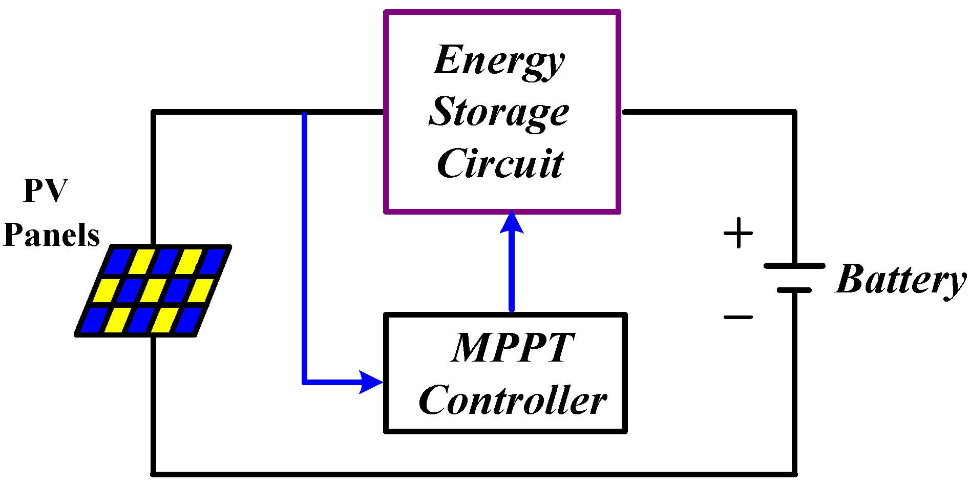
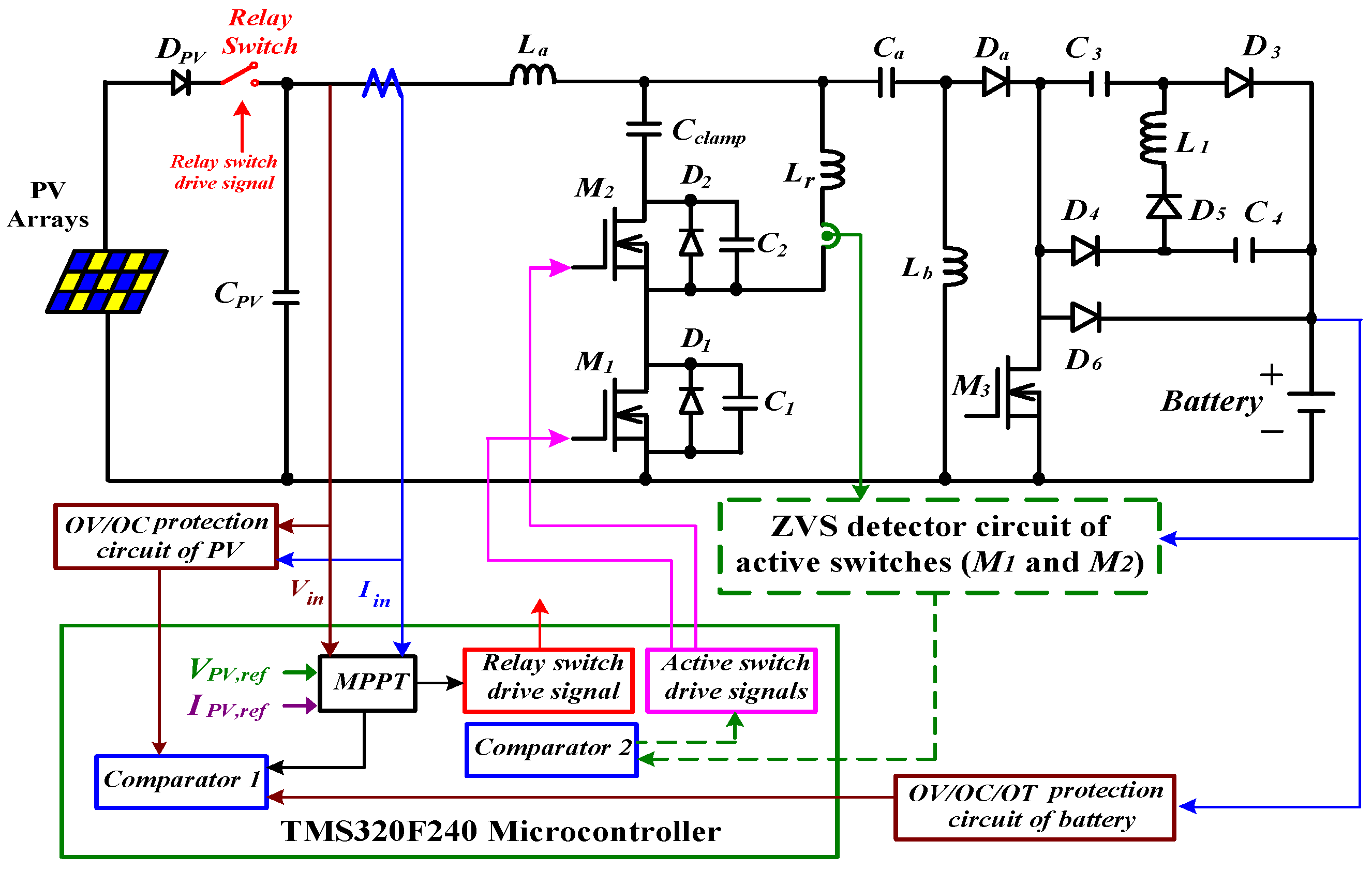
3. Control Scheme Description
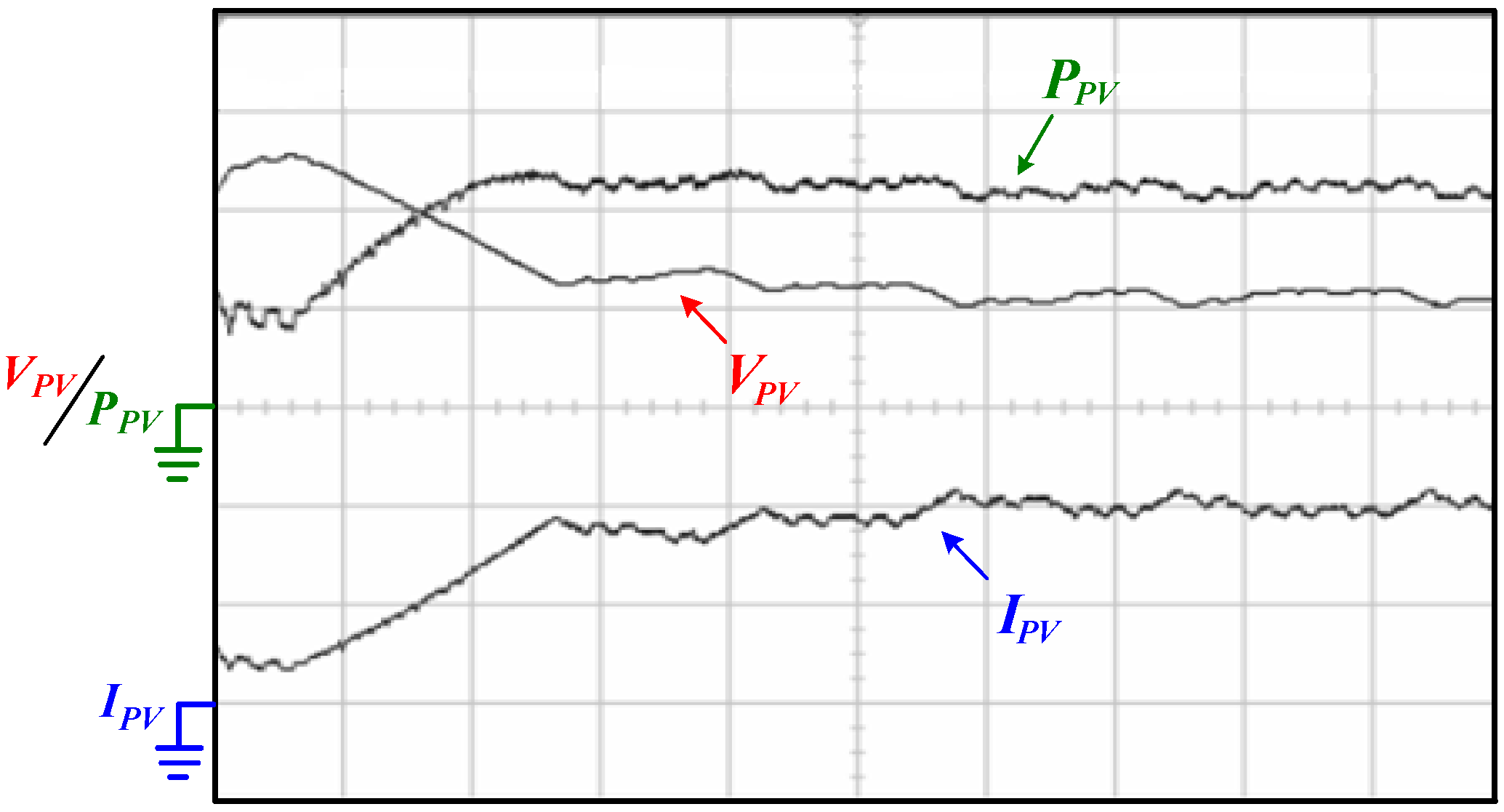
3.1. Description of the MPPT Algorithm


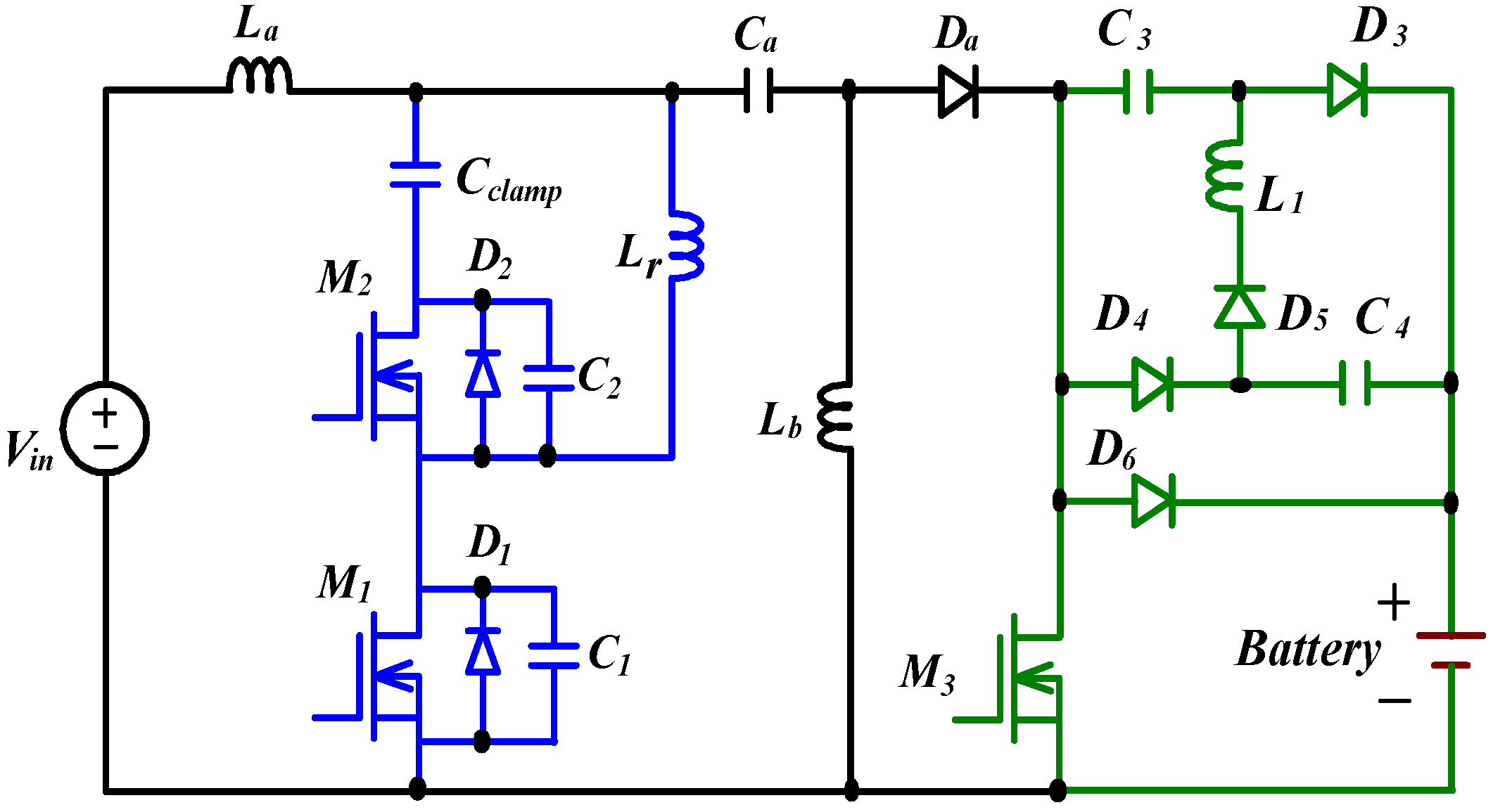
3.2. ZVS Cell Description
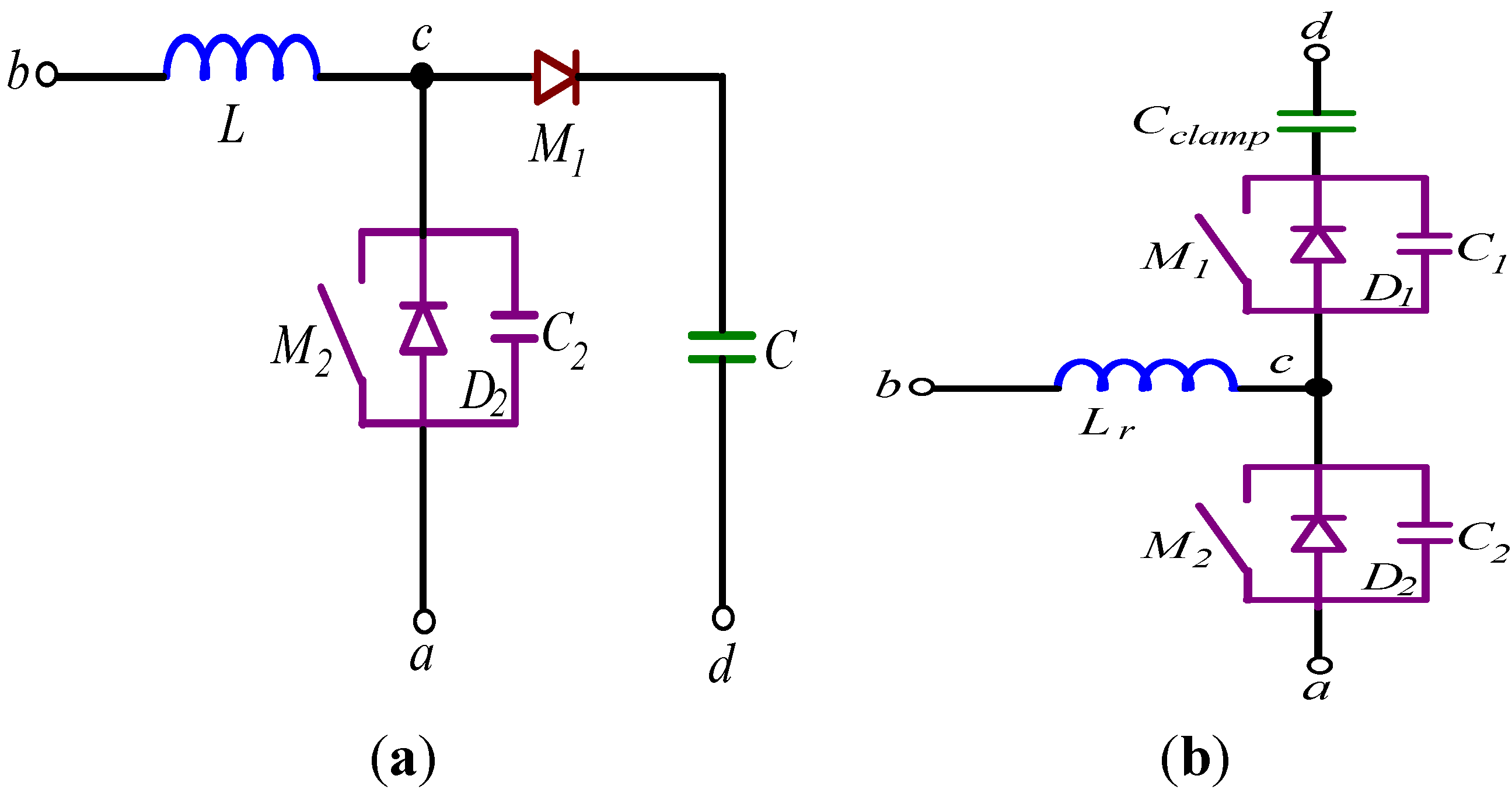
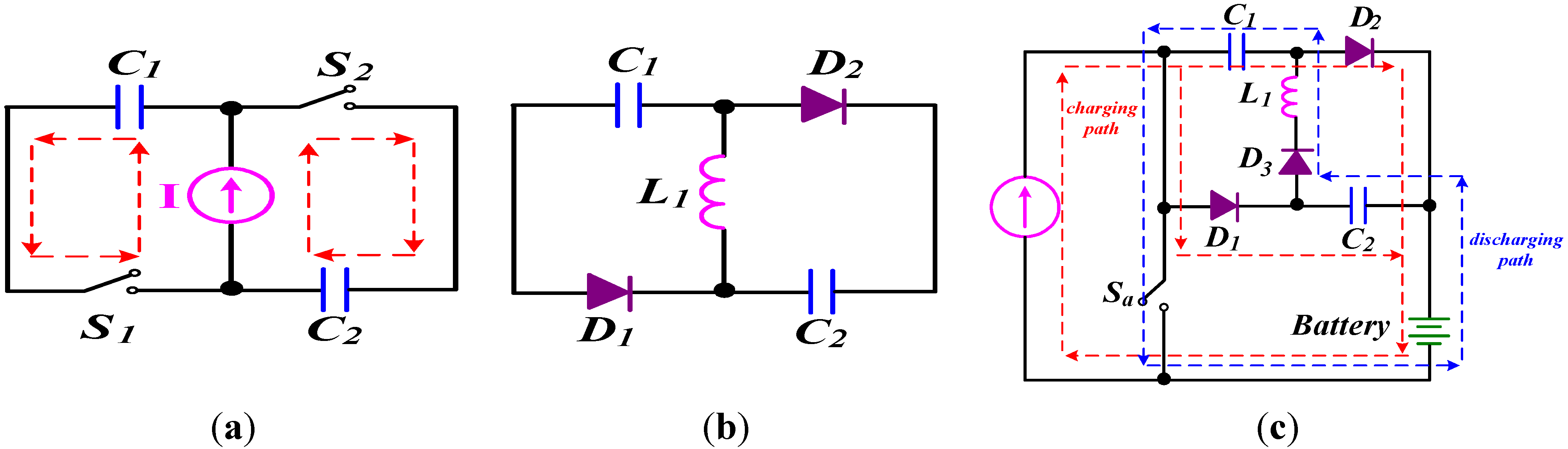
3.3. Description of a Non-Dissipative Charging/Discharging Reflex Cell

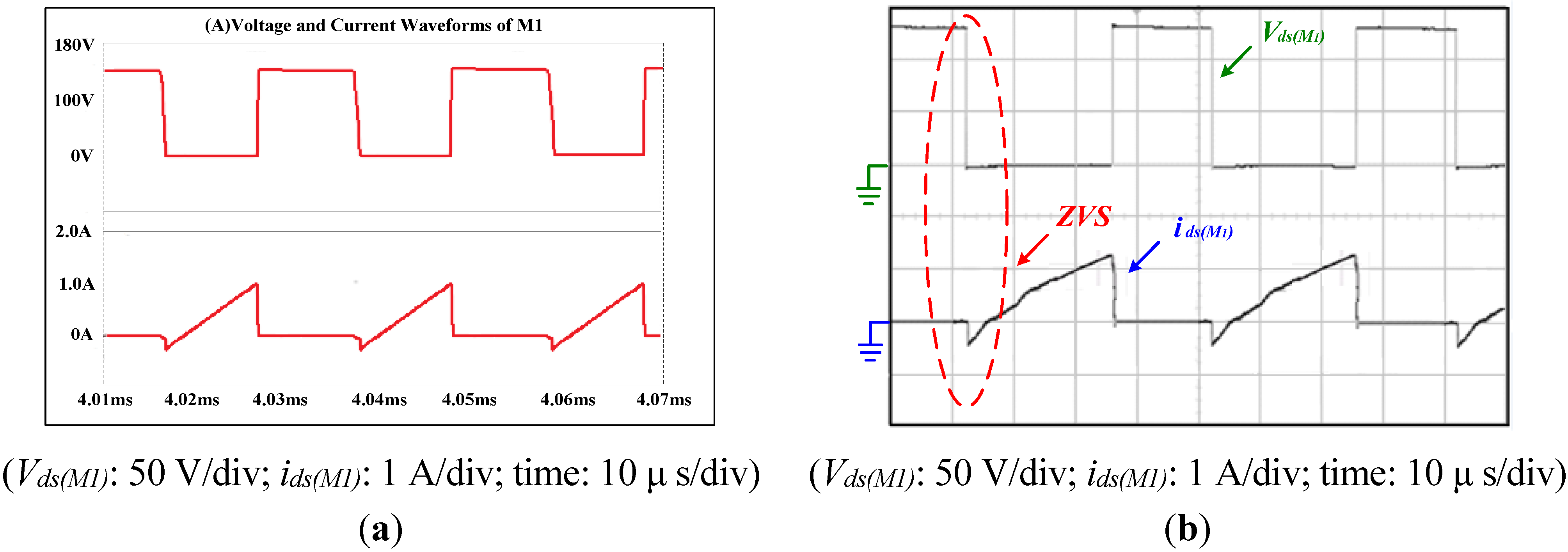
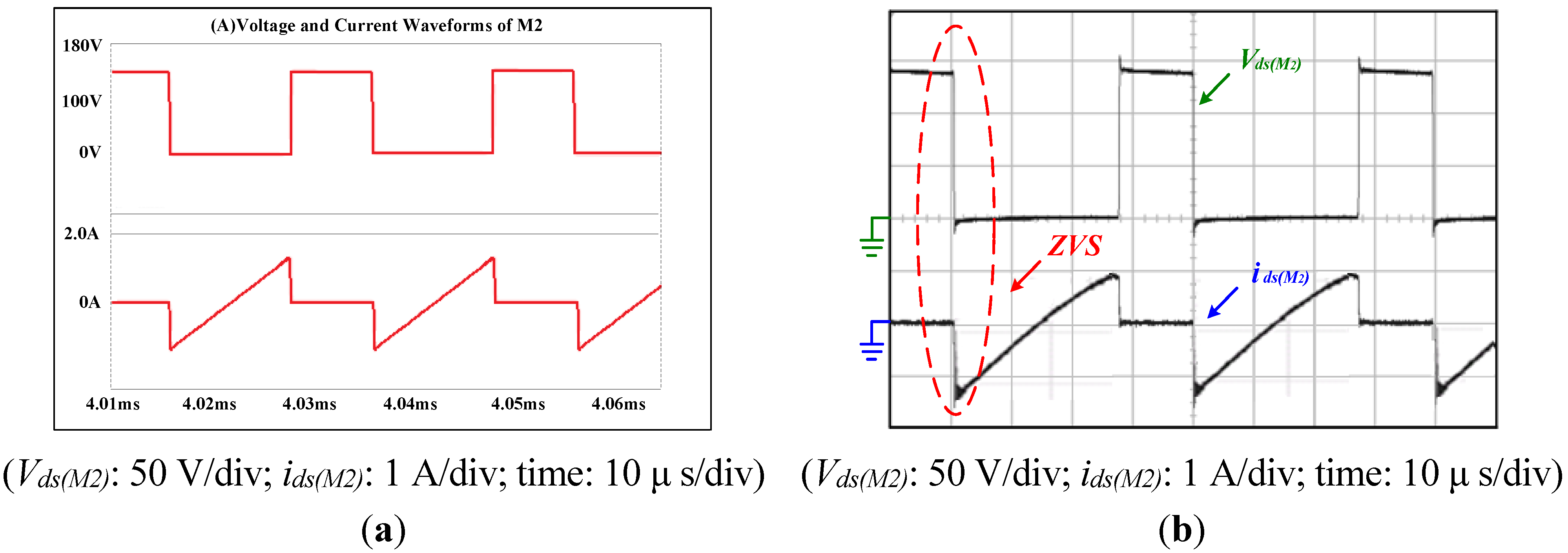
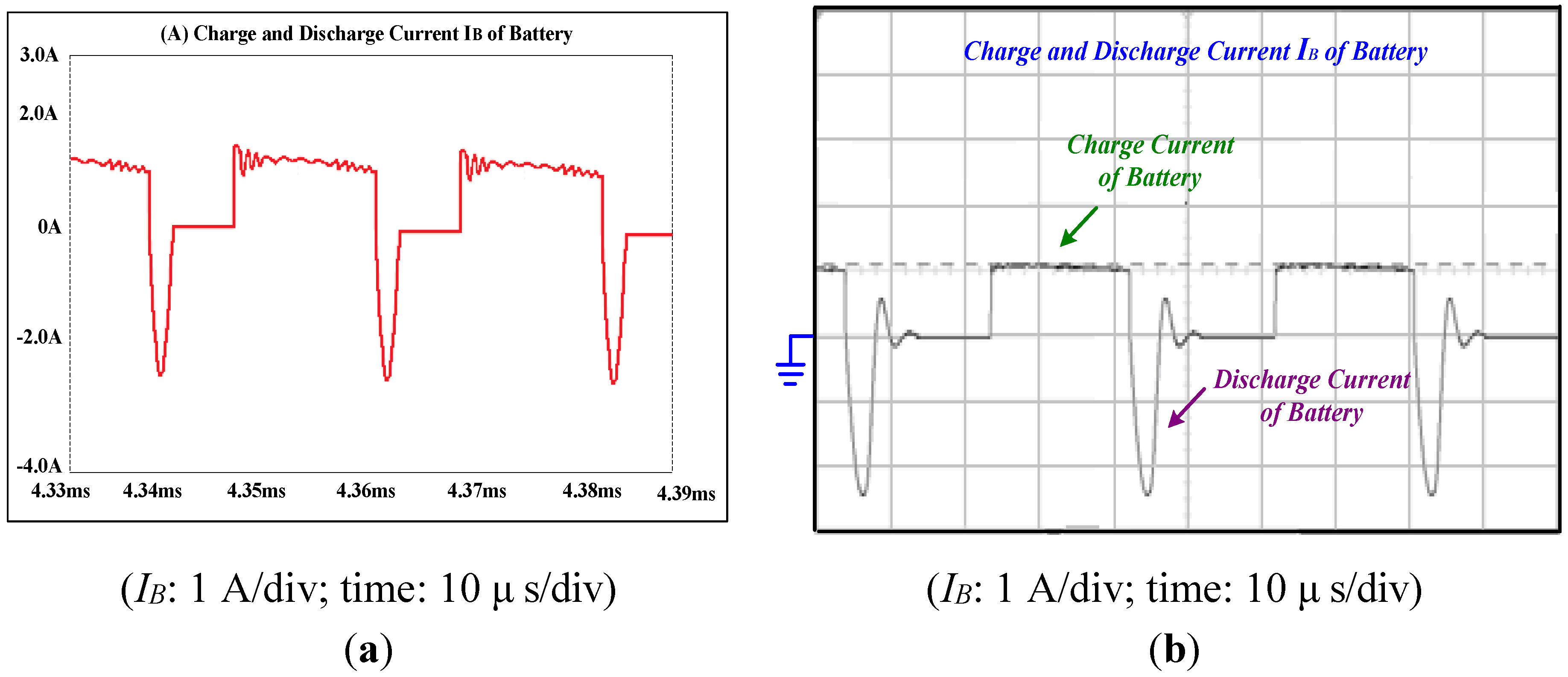
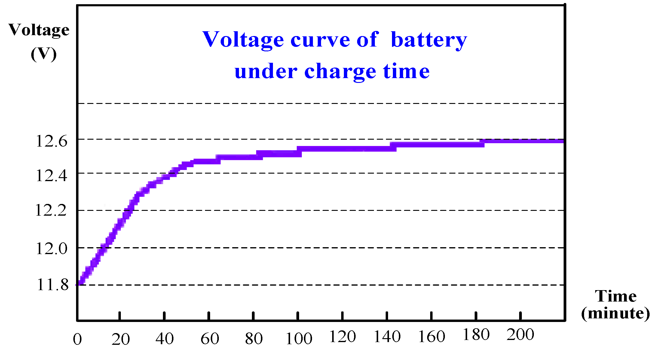
4. Experimental Results
- Voltage of PV arrays: Vpv = 100 Vdc;
- Voltage of Lead-Acid battery: VB = 12 Vdc, capacity = 4 Ah;
- Maximum charging current of Lead-Acid battery: IB = 2 A;
- Inductor La = Lb = 3 mH;
- Inductor L1 = 5 μH;
- Resonant inductor Lr = 5 μH;
- Capacitor C3 =C4 = 300 nF; and
- Switching frequency (M1 and M2): fs = 50 kHz.
5. Conclusions
Acknowledgments
Author Contributions
Conflicts of Interest
References
- Bull, S.R. Renewable energy today and tomorrow. Proc. IEEE 2001, 89, 1216–1226. [Google Scholar] [CrossRef]
- World Wind Energy Association. World Wind Energy Report 2008; World Wind Energy Association: Bonn, Germany, 2009. [Google Scholar]
- Ahmed, K.H.; Finney, S.J.; Williams, B.W. Fuzzy-logic-control approach of a modified hill-climbing method for maximum power point in microgrid standalone photovoltaic system. IEEE Trans. Power Electron. 2011, 26, 1022–1030. [Google Scholar] [CrossRef]
- Tseng, S.-U.; Tsai, C.-T. Photovoltaic power system with an interleaving boost converter for battery charger applications. Int. J. Photoenergy 2012, 2012, 1–15. [Google Scholar]
- Chao, K.H.; Chang, L.Y.; Liu, H.C. Maximum-power-point-tracking method based on modified particle swarm optimization for photovoltaic systems. Int. J. Photoenergy 2013, 2013, 1–6. [Google Scholar]
- Tang, K.H.; Chao, K.H.; Chao, Y.W.; Chen, J.P. Design and implementation of a simulator for photovoltaic modules. Int. J. Photoenergy 2012, 2012, 1–8. [Google Scholar]
- Kuo, Y.-C.; Liang, T.-J.; Chen, J.-F. Novel maximum-power-point-tracking controller for photovoltaic energy conversion system. IEEE Trans. Ind. Electron. 2001, 48, 594–601. [Google Scholar] [CrossRef]
- Koyanagi, A.; Nakamura, H.; Kobayashi, M.; Suzuki, Y. Study on maximum power point tracking of wind turbine generator using a flywheel. Proc. Power Convers. 2002, 1, 322–327. [Google Scholar]
- Amei, K.; Takayasu, Y.; Ohji, T.; Sakui, M. A maximum power control of wind generator system using a permanent magnet synchronous generator and a boost chopper circuit. Proc. Power Convers. 2002, 3, 1447–1452. [Google Scholar]
- Shen, C.-L.; Tsai, C.-T. Double-linear approximation algorithm to achieve maximum-power-point tracking for photovoltaic arrays. Energies 2012, 5, 1982–1997. [Google Scholar] [CrossRef]
- Teleke, S.; Baran, M.E.; Huang, A.Q.; Bhattacharya, S.; Anderson, L. Control strategies for battery energy storage for wind farm dispatching. IEEE Trans. Energy Convers. 2009, 24, 725–731. [Google Scholar] [CrossRef]
- Cao, J.; Schofield, N.; Emadi, A. Battery balancing methods: A comprehensive review. In Proceedings of the IEEE Vehicle Power and Propulsion Conference, Harbin, China, 3–5 September 2008.
- Chiu, H.-J.; Lin, L.-W.; Pan, P.-L.; Tseng, M.-H. A novel rapid charger for lead-acid batteries with energy recovery. IEEE Trans. Power Electron. 2006, 21, 640–647. [Google Scholar] [CrossRef]
- Hsieh, Y.C.; Moo, C.S.; Wu, C.K.; Cheng, J.C. A non-dissipative reflex charging circuit. In Proceeding of the 25th International Telecommunications Energy Conference, INTELEC ’03, Yokohama, Japan, 23–23 October 2003; pp. 679–683.
- Chen, L.-R.; Chu, N.-Y.; Wang, C.-S.; Liang, R.-H. Design of a reflex-based bidirectional converter with the energy recovery function. IEEE Trans. Ind. Electron. 2008, 55, 3022–3029. [Google Scholar] [CrossRef]
- Zhang, J.; Yu, J.; Cha, C.; Yang, H. The effects of pulse charging on inner pressure and cycling characteristics of sealed Ni/MH batteries. J. Power Sources 2004, 136, 180–185. [Google Scholar] [CrossRef]
- Yabuta, K.; Matsushita, T.; Tsujikawa, T. Examination of the cycle life of valve regulated lead acid batteries. In Proceedings of the 29th International Telecommunications Energy Conference, INTELEC 2007, Rome, Italy, 30 September–4 October 2007; pp. 97–101.
- Tsai, C.-T. Energy storage system with voltage equalization strategy for wind energy conversion. Energies 2012, 5, 2331–2350. [Google Scholar]
- Patel, H.; Agarwal, V. MPPT scheme for a PV-fed single-phase single-stage grid-connected inverter operating in CCM with only one current sensor. IEEE Trans. Energy Convers. 2009, 24, 256–263. [Google Scholar] [CrossRef]
- Moore, S.W.; Schneider, P.J. A review of cell equalization methods for lithium ion and lithium polymer battery system. In Proceedings of the SAE 2001 World Congress, Detroit, MI, USA, 12 March 2001.
- Lee, Y.S.; Chen, G.T. ZCS bi-directional DC-to-DC converter application in battery equalization for electric vehicles. In Proceedings of the IEEE Power Electronics Specialists Conference, Rhodes, Greece, 15–19 June 2004; Volume 4, pp. 2766–2772.
- Lee, Y.S.; Chen, M.-W.; Hsu, K.-L.; Du, J.-Y.; Chuang, C.-F. Cell equalization scheme with energy transferring capacitance for series connected battery strings. In Proceedings of the IEEE TenCon’02, 2002 IEEE Region 10 Conference on Computers, Communications, Control and Power Engineering, Beijing, China, 28–31 October 2002; pp. 2042–2045.
- Cho, J.G.; Baek, J.W.; Yoo, D.W.; Lee, H.S.; Rim, G.H. Novel zero-voltage and zero-current-switching full bridge PWM converter using transformer auxiliary winding. IEEE Trans. Power Electron. 2000, 15, 250–257. [Google Scholar] [CrossRef]
- Lo, Y.K.; Kao, T.S.; Lin, J.K. Analysis and design of an interleaved active-clamp forward converter. IEEE Trans. Ind. Electron. 2007, 54, 2323–2332. [Google Scholar] [CrossRef]
© 2015 by the authors; licensee MDPI, Basel, Switzerland. This article is an open access article distributed under the terms and conditions of the Creative Commons Attribution license (http://creativecommons.org/licenses/by/4.0/).
Share and Cite
Tsai, C.-T.; Kuo, Y.-C.; Kuo, Y.-P.; Hsieh, C.-T. A Reflex Charger with ZVS and Non-Dissipative Cells for Photovoltaic Energy Conversion. Energies 2015, 8, 1373-1389. https://doi.org/10.3390/en8021373
Tsai C-T, Kuo Y-C, Kuo Y-P, Hsieh C-T. A Reflex Charger with ZVS and Non-Dissipative Cells for Photovoltaic Energy Conversion. Energies. 2015; 8(2):1373-1389. https://doi.org/10.3390/en8021373
Chicago/Turabian StyleTsai, Cheng-Tao, Ying-Che Kuo, Ying-Piao Kuo, and Chin-Tsung Hsieh. 2015. "A Reflex Charger with ZVS and Non-Dissipative Cells for Photovoltaic Energy Conversion" Energies 8, no. 2: 1373-1389. https://doi.org/10.3390/en8021373