Mass Production Test of Solar Cells and Modules Made of 100% UMG Silicon. 20.76% Record Efficiency

Abstract
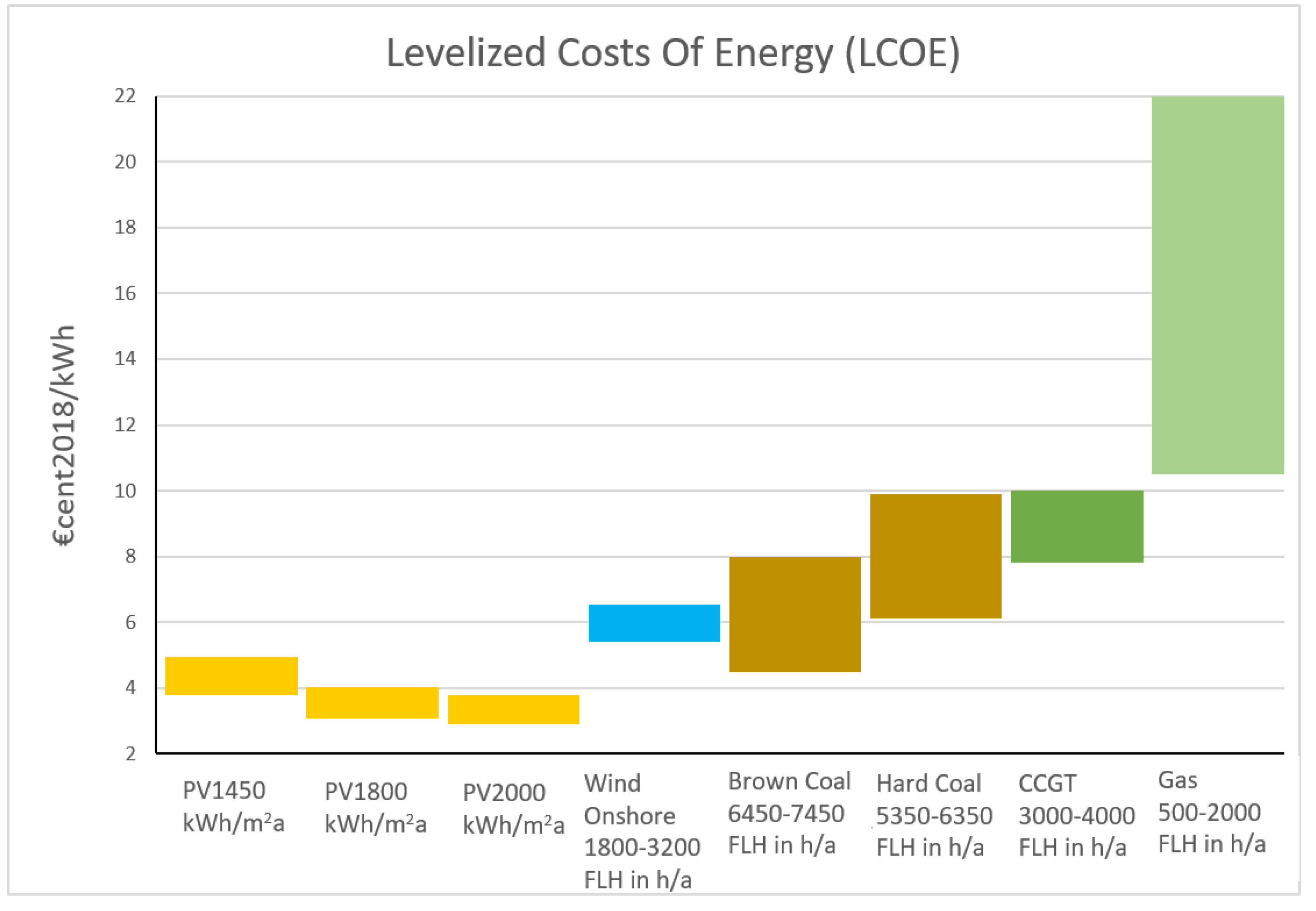
:1. Introduction
- Diamond-Wire Saw (DWS), introduced to the market gradually during the past 5 years, is considered a disruptive wafer sawing technology due to its lower costs of ownership and the higher throughput (around 60 wafers per kg of certified silicon) compared to traditional Slurry Cut Wire Saw (SWS). Nevertheless, while those advantages have been applied effectively to monocrystalline ingots, the throughput for multicrystalline has been slightly less (around 55 wafers per kg) than in mono. Moreover, the multicrystalline technology has suffered from problems of texturization due to the soft wafer surface resulting from the DWS.
- PERC: The implementation of high efficiency cell architectures as Passivated Emitter and Rear Cell has also adversely affected the multicrystalline technology variant. Due to the optimization of surface passivation of the cells, the bulk lifetime, lower in multi than in mono, has become the limiting factor of cell efficiency.
- LeTID or CID: The Light at elevated Temperature Induced Degradation (LeTID) or the Current Induced Degradation (CID) has become a deleterious effect on multicrystalline PERC solar cells. It results in a deep degradation of performance of the module once installed in real outdoor conditions [2]. Boron oxide complexes (B-O) or iron boron pairs (FeB) cannot be considered responsible for LeTID or CID, as they are for Light Induced Degradation (LID). It is currently assumed that hydrogen introduced for passivation plays an important role in this degradation [3].
- ePDG: Phosphorus diffusion gettering happens naturally during the emitter diffusion step of the conventional p-type cell process flow, improving the bulk minority carrier lifetime significantly. Since the 1970s, phosphorus doping is done at industrial level using POCl3 thermal diffusion [4]. The main advantages of this technology are the low operational costs and the commercial readily availability of high-throughput equipment. Normally, phosphorus diffusion is carried out in two steps, first a phosphosilicate glass (PSG) layer is deposited on the surface of the wafer and afterwards the phosphorus is forced to move deeper in a drive-in step, which is carried out at a lower temperature and without the feeding of the phosphorus source. The impurity gettering happens in the phosphorus diffusion and other thermal steps of cell processing, such as passivation [5], low thermal annealing (LTA) or contacts co-firing [6]. This phenomenon is responsible for the better bulk lifetime and emitter recombination properties of the processed material when compared to the as-grown material. Nevertheless, it is a complex phenomenon in which several competing mechanisms take place [7], including internal impurities gettering (migration to grain boundaries, dislocation or precipitates), external impurities gettering (migration to the surface), defects reconfiguration or bulk passivation of defects or changes in the surface recombination velocity (by hydrogen for example, during SiNx layer formation). In the case of UMG-Si, and other solar grade materials obtained by metallurgical purification, the presence of impurities, especially iron, is higher than in a p-type multicrystalline silicon made from polysilicon. This element is mainly present in the form of interstitial iron and can be significantly reduced by the application of tailored process parameters [8,9], without increasing neither the overall cost nor the complexity of the operations. In our case an “extended” PDG (or ePDG) should be used, encompassing engineering intervention in all the thermal processes during solar cells production in addition to phosphorus diffusion.
- B-Si: Black silicon is being introduced in a massive scale into production lines [10]. Due to the reduction of reflection, B-Si has been able to increase the absolute efficiency of multicrystalline solar cells up to 0.4 %abs [11]. Moreover, according to Pasanen et al. [12], both PDG and B-Si techniques in combination, have additive and synergetic effects that potentiate each other, opening the possibility of using metallurgically refined silicon to high efficiency solar cells. The combination of B-Si and PDG together with the usage of high-quality silicon purified by metallurgical route, also known as upgraded metallurgical grade silicon (UMG-Si), can contribute to lower production cost of PV ($/kWp). Pasanen et al. have also published the positive impact of B-Si on solar cells in terms of Current Induced Degradation, which emphasizes even more the possibilities of UMG-Si [3]. Under an economical assessment, Modanese et al. [13] calculated a relative cost reduction of up to 11.7% for a multicrystalline B-Si + PERC solar cell compared with a monocrystalline PERC solar cell, being most of the reduction related to feedstock and ingot growing.
- LeTID recovery or current induced recovery (CIR): There are several techniques that can mitigate or even eliminate the LeTID or CID of the cells. Most of these consist in applying temperature, current or light [14,15,16]. In fact, CIR has been already tested industrially and implemented successfully in productions lines. This method accelerates the LeTID, that typically takes thousands of hours, and provokes the final recovery of the solar cells that would otherwise takes place naturally in the field only after several months.
- Mono-like: This silicon growth technology was already introduced in the industry in 2012 [17] with good results in terms of quality, but suffered of structure inhomogeneity along the ingot height. This, together with the cost of the seeds and the rapid and successful introduction of the high performance multicrystalline (HPM) growth technique, kept the mono-like (also called mono-cast) out of the business. Nevertheless, companies among the PV leaders are currently revisiting and adopting this technology [18], indicating that the previous drawbacks can be overcome.
2. Materials and Methods
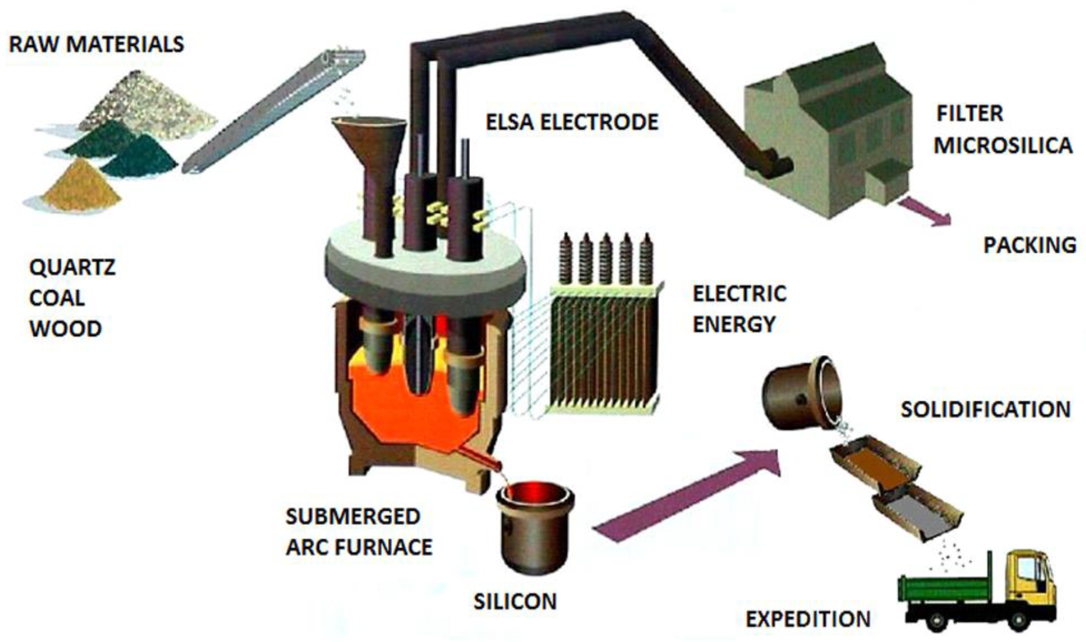
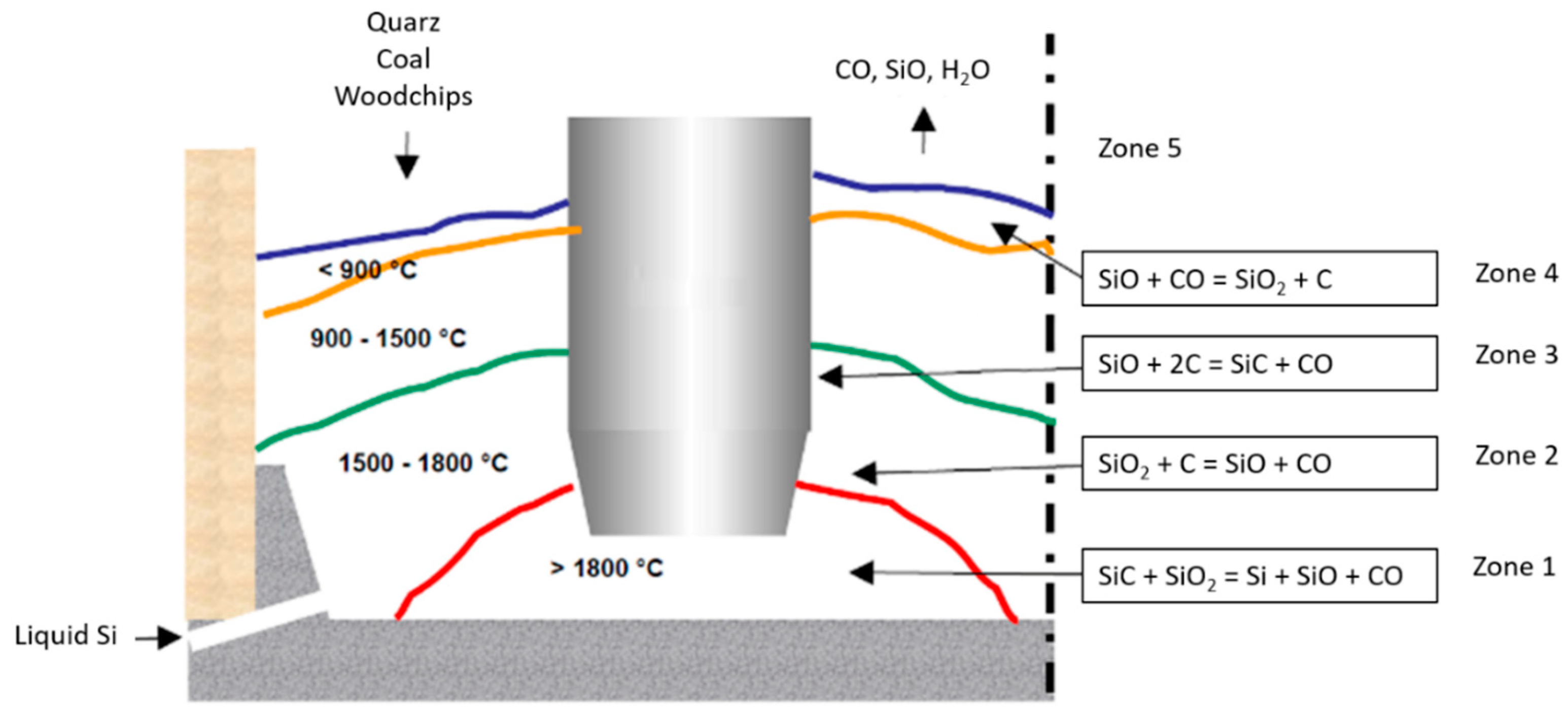
2.1. Carbo-Reduction to Obtain MeG-Si
- Metals (principally Fe, Al, Ca followed by Ti, Mn and traces of transition metal): 1 to 4%
- Boron: 8–50 ppmw
- Phosphorus: 10–50 ppmw
2.2. Silicon Purification
2.2.1. Slagging
2.2.2. Vacuum Refining
2.2.3. Directional Solidification
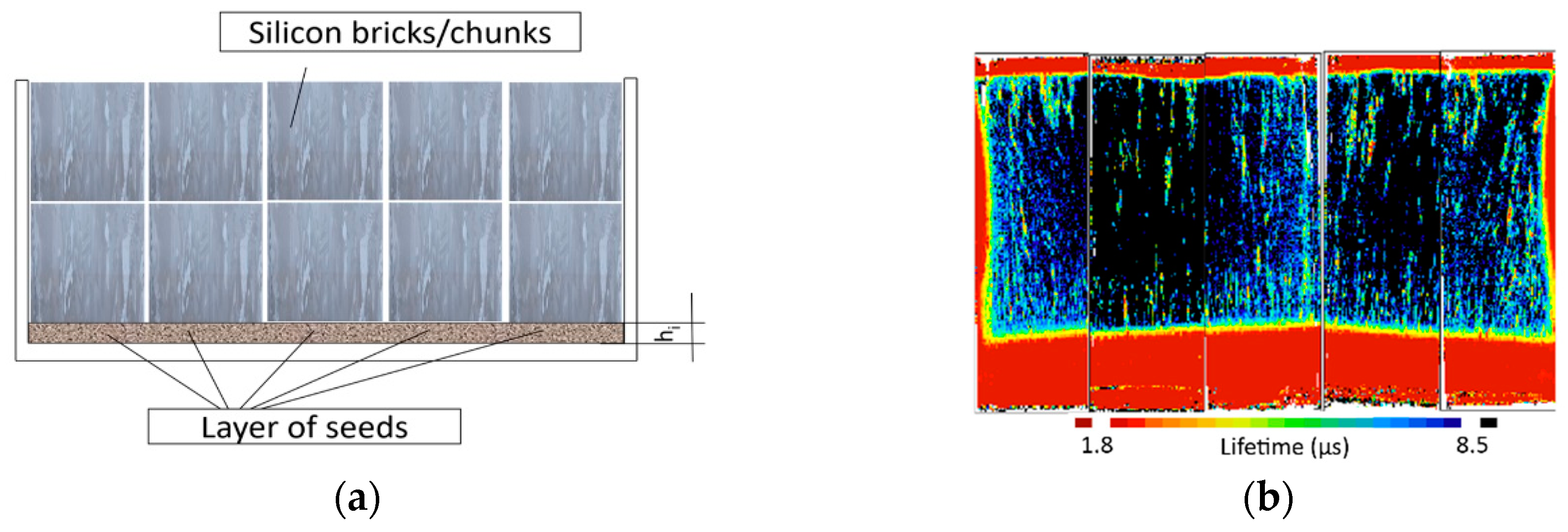
- P-type silicon bricks and chunks
- [B] < 0.2 ppmw
- [P] = 0.1–0.3 ppmw (the concentration of P is tuned to compensate the boron)
- ∑[Me] < 0.5 ppmw (Me being Fe, Al, transition, alkaline and alkaline earth elements).
2.3. Ingot Growing and Wafering
2.4. Solar Cells Production
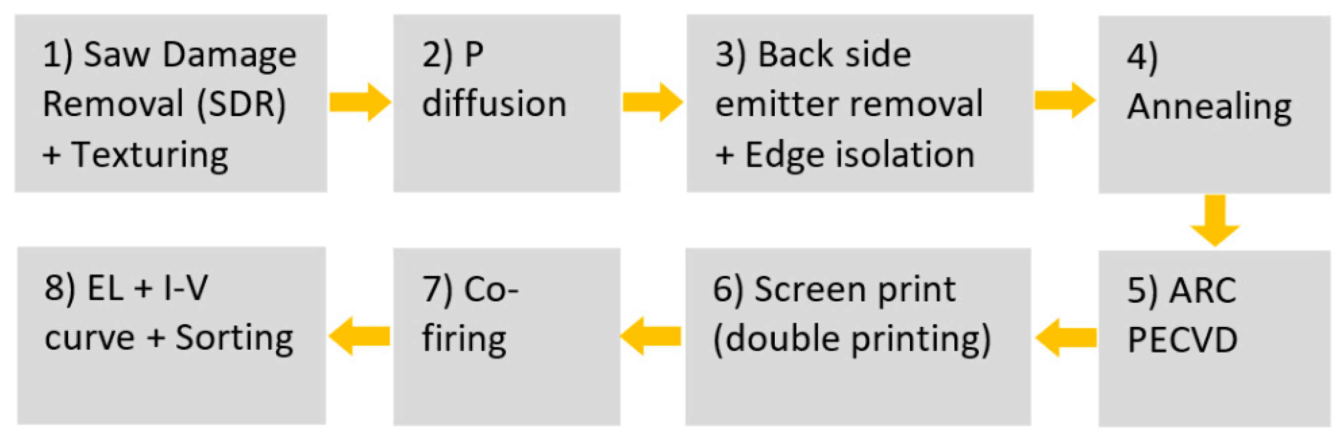
2.4.1. Al-BSF Cells
- The first stage consists in a nitric and hydrofluoric acid etching for surface cleaning, saw damage removal and texturing.
- The wafers are placed back to back to be introduced into quartz furnaces to perform a Low Pressure Chemical Vapor Deposition (LPCVD) of a thin film of phosphosilicate glass (PSG) composed of (P2O5)x(SiO2)1−x.
- In the next step the diffused phosphorus from the back side is removed. For that, a back side chemical etching is performed, followed by a rinse in another chemical etching to achieve the edge isolation and avoid the edge shunts.
- Annealing is a pre-treatment process prior to antireflective coating (ARC) of silicon nitride. In this short process a thin film of silicon dioxide is deposited to increase the Potential Induced Degradation resistance of the solar cell, what is commercially called PID free solar cells [37].
- Antireflective Coating (ARC). Silicon nitride (SiNx:H) coating of approximately 75 nm thick is deposited on the front surface by means of a Plasma Enhanced Chemical Vapor Deposition reactor (PECVD) to increase light absorption. This coating is also suited for surface passivation due to the field effect passivation [38]. The Hydrogen present in the silicon nitride coating is also involved in a chemical passivation [39].
- Front and rear contacts as well as the Aluminum coating responsible for the Back Surface Field (BSF) formation are printed in a double printing process, saving Ag consumption and reducing the shadow losses [40].
- Co-firing furnace is used to make the drive through of the contacts [41].
- In the last step of the solar cells production, the solar cells undergo an electroluminescence test (EL test) [42] where a defect detection software is used.
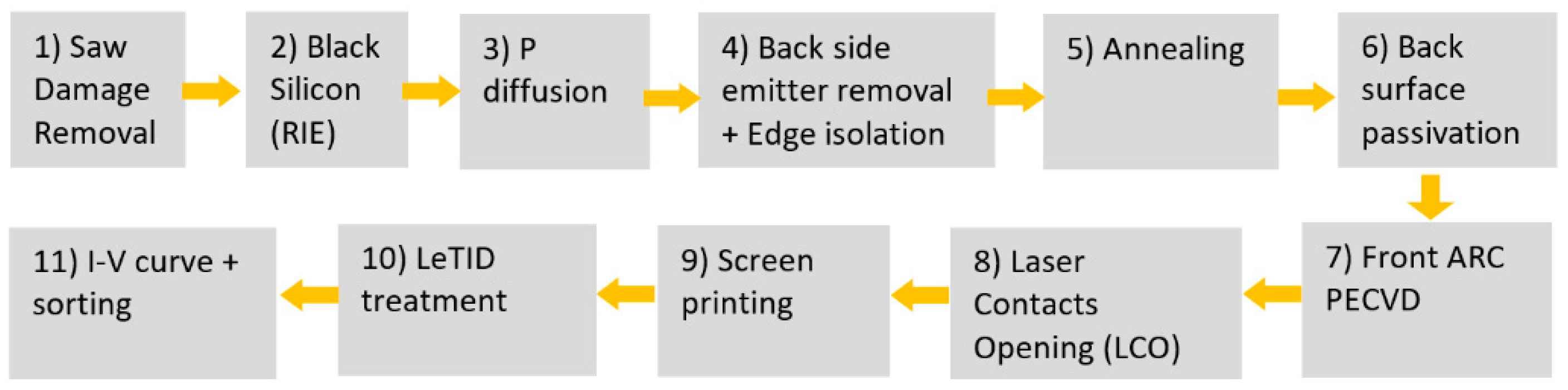
2.4.2. Black Silicon + PERC Cells
- 2) Black silicon (B-Si) nano-texture. The technology used to provoke a nano-texture on top of the wafer is reactive ion etching (RIE). SF6 and O2 gases are introduced into the reaction chamber. In there, a synergetic mechanism of chemical etching, passivation and ion bombardment takes place, thus, nano-structures are formed reducing considerably the reflectance of the wafer [10,43].
- 6) Back surface passivation. To reduce the back surface recombination a passivation layer is deposited in the back surface which gives name to the passivated emitter and rear cells (PERC) [44,45]. In this test, an Al2O3 film is deposited onto the back surface, acting as a passivating agent. After the oxide deposition, a capping layer of silicon nitride was deposited. The role of this capping layer is to behave as a back reflector for long wavelength radiation as well as being a barrier for Al metal contacts. Also, this silicon nitride reduces the surface recombination velocity due to its negative charge [46]. Both films were deposited by means of PECVD.
- 8) Laser Contacts Opening. Backside openings through the passivation stack were made by a nanosecond pulsed laser.
2.5. PV Modules Production
3. Results and Discussion
Author Contributions
Funding
Conflicts of Interest
References
- Kost, C.; Shammugam, S.; Jülch, V.; Nguyen, H.-T.; Schlegl, T.; Mayer, J.N.; Thomsen, J.; Hartmann, N.; Senkpiel, C.; Philipps, S.; et al. Levelized Cost of Electricity: Renewable Energy Technologies; Fraunhofer ISE: Freiburg, Germany, 2018. [Google Scholar]
- Kersten, F.; Engelhart, P.; Ploigt, H.-C.; Stekolnikov, A.; Lindner, T.; Stenzel, F.; Bartzsch, M.; Szpeth, A.; Petter, K.; Heitmann, J.; et al. Degradation of multicrystalline silicon solar cells and modules after illumination at elevated temperature. Sol. Energy Mater. Sol. Cells 2015, 142, 83–86. [Google Scholar] [CrossRef]
- Pasanen, T.P.; Modanese, C.; Vähänissi, V.; Laine, H.S.; Wolny, F.; Oehlke, A.; Kusterer, C.; Heikkinen, I.T.S.; Wagner, M.; Savin, H. Impact of black silicon on light- and elevated temperature-induced degradation in industrial passivated emitter and rear cells. Prog. Photovolt. Res. Appl. 2018. [Google Scholar] [CrossRef]
- Li, H.; Kim, K.; Hallam, B.; Hoex, B.; Wenham, S.; Abbott, M. POCl3 diffusion for industrial Si solar cell emitter formation. Front. Energy 2017, 11, 42–51. [Google Scholar] [CrossRef]
- Hallam, B.; Chen, D.; Kim, M.; Stefani, B.; Hoex, B.; Abbott, M.; Wenham, S. The role of hydrogenation and gettering in enhancing the efficiency of next-generation Si solar cells: An industrial perspective. Phys. Status Solidi Appl. Mater. Sci. 2017, 214, 1700305. [Google Scholar] [CrossRef]
- Peral, A.; Dastgheib-Shirazi, A.; Fano, V.; Jimeno, J.C.; Hahn, G.; del Canizo, C. Impact of Extended Contact Cofiring on Multicrystalline Silicon Solar Cell Parameters. IEEE J. Photovolt. 2017, 7, 91–96. [Google Scholar] [CrossRef]
- Al-Amin, M.; Murphy, J.D. Passivation effects on low-temperature gettering in multicrystalline silicon. IEEE J. Photovolt. 2017, 7, 68–77. [Google Scholar] [CrossRef]
- Jiménez, A.; del Cañizo, C.; Cid, C.; Peral, A. Phosphorus Diffusion Gettering Efficacy in Upgraded Metallurgical-Grade Solar Silicon. J. Electron. Mater. 2018, 47, 5068–5071. [Google Scholar] [CrossRef]
- Kohler, D.; Raabe, B.; Braun, S.; Seren, S.; Hahn, G. Upgraded metallurgical grade silicon solar cells : A detailed material analysis. In Proceedings of the 24th European Photovoltaic Solar Energy Conference, Hamburg, Germany, 21–24 September 2009; pp. 1758–1761. [Google Scholar]
- Rentsch, J.; Kafle, B.; Hofmann, M.; Krieg, K.; Zimmer, M. Texture etching technologies for diamond-wire-sawn mc-Si solar cells. Photovolt. Int. 2017, 38, 56–66. [Google Scholar]
- Wang, X.; Zou, S.; Xing, G. 19.31%-efficiency multicrystalline silicon solar cells using MCCE black silicon technology. Photovolt. Int. 2017, 35, 67–72. [Google Scholar]
- Pasanen, T.P.; Laine, H.S.; Vähänissi, V.; Schön, J.; Savin, H. Black silicon significantly enhances phosphorus diffusion gettering. Sci. Rep. 2018, 8, 1991. [Google Scholar] [CrossRef] [PubMed]
- Modanese, C.; Laine, H.; Pasanen, T.; Savin, H.; Pearce, J. Economic Advantages of Dry-Etched Black Silicon in Passivated Emitter Rear Cell (PERC) Photovoltaic Manufacturing. Energies 2018, 11, 2337. [Google Scholar] [CrossRef]
- Bredemeier, D.; Walter, D.C.; Pernau, T.; Romer, O.; Schmidt, J. Production compatible remedy against LETID in high-performance multicrystalline silicon solar cells. In Proceedings of the 35th European Photovoltaic Solar Energy Conference and Exhibition, Brussels, Belgium, 24–28 September 2018; pp. 406–409. [Google Scholar]
- Wu, J.; Yao, Z.; Zhang, D.; Xiong, G.; Jiang, F.; Sun, J.; Jaubert, J.-N.; Xing, G. Industrial Solutions to Mitigate Light-Induced Degradation in mc-PERC Cells and Modules. In Proceedings of the 35th European Photovoltaic Solar Energy Conference and Exhibition (EU PVSEC), Brussels, Belgium, 24–28 September 2018; pp. 835–838. [Google Scholar]
- Jiang, F.; Jaubert, J.N.; Zhang, D.; Yao, Z.; Xiong, G.; Wu, J.; Xing, G. Solutions to realizing LID-controlled multi-PERC cells and modules. Photovolt. Int. 2018, 40, 57–62. [Google Scholar]
- Guerrero, I.; Parra, V.; Carballo, T.; Black, A.; Miranda, M.; Cancillo, D.; Moralejo, B.; Jiménez, J.; Lelièvre, J.-F.; del Cañizo, C. About the origin of low wafer performance and crystal defect generation on seed-cast growth of industrial mono-like silicon ingots. Prog. Photovolt. Res. Appl. 2014, 22, 923–932. [Google Scholar] [CrossRef]
- GCL Produces High-Efficiency Module to Power 13 Million Homes. Available online: https://www.prnewswire.com/in/news-releases/gcl-produces-high-efficiency-module-to-power-13-million-homes-694341171.html (accessed on 21 March 2019).
- EU PVSEC: “Multicrystalline Silicon Will Not Die”—PV Magazine International. Available online: https://www.pv-magazine.com/2018/09/28/eu-pvsec-multicrystalline-silicon-will-not-die/ (accessed on 21 March 2019).
- TÜV Rheinland Solar Energy. Factory Inspections to Confirm Raw Material Traceability of Silicon Used for Photovoltaic Module Production for FerroAtlántica; TÜV Rheiland: Cologne, Germany, 2018. [Google Scholar]
- Schei, A.; Tuset, J.K.; Tveit, H. Production of High Silicon Alloys; Tapir: Trondheim, Norway, 1998; ISBN 9788251913171. [Google Scholar]
- Forniés, E.; Méndez, L.; Tojeiro, M. Polysilicon vs. upgraded metallurgical silicon (UMG-Si): Technology, quality and costs. Photovolt. Int. 2016, 31, 29–38. [Google Scholar]
- Hopkins, R.H.; Rohatgi, A. Impurity effects in silicon for high efficiency solar cells. J. Cryst. Growth 1986, 75, 67–79. [Google Scholar] [CrossRef]
- Jakobsson, L.K.; Tangstad, M. Distribution of Boron between Silicon and CaO-MgO-Al2O3-SiO2 Slags. Metall. Mater. Trans. B 2014, 45, 1644–1655. [Google Scholar] [CrossRef]
- Safarian, J.; Tranell, G.; Tangstad, M. Thermodynamic and Kinetic Behavior of B and Na through the Contact of B-Doped Silicon with Na2O-SiO2 Slags. Metall. Mater. Trans. B 2013, 44, 571–583. [Google Scholar] [CrossRef]
- Altenberend, J. Kinetics of the Plasma Refining Process of Silicon for Solar Cells: Experimental Study with Spectroscopy. Ph.D. Thesis, University of Grenoble, Grenoble, France, 2013. [Google Scholar]
- Nordstrand, E.F.; Tangstad, M. Removal of Boron from Silicon by Moist Hydrogen Gas. Metall. Mater. Trans. B 2012, 43, 814–822. [Google Scholar] [CrossRef]
- Sortland, Ø.S. Boron Removal from Silicon by Steam and Hydrogen. Ph.D. Thesis, NTNU, Trondheim, Norway, 2015. [Google Scholar]
- Al-Khazraji, R.; Li, Y.; Zhang, L. Application of slag refining technique to metallurgical grade silicon purification process: A review. Funct. Mater. 2018, 25, 364–370. [Google Scholar] [CrossRef]
- Miki, T.; Morita, K.; Sano, N. Thermodynamics of phosphorus in molten silicon. Metall. Mater. Trans. B 1996, 27, 937–941. [Google Scholar] [CrossRef]
- Schlesinger, M.E. The Thermodynamic Properties of Phosphorus and Solid Binary Phosphides. Chem. Rev. 2002, 102, 4267–4302. [Google Scholar] [CrossRef] [PubMed]
- Zheng, S.-S.; Abel Engh, T.; Tangstad, M.; Luo, X.-T. Separation of Phosphorus from silicon by induction vacuum refining. Sep. Purif. Technol. 2011, 82, 128–137. [Google Scholar] [CrossRef]
- Safarian, J.; Tangstad, M. Vacuum Refining of Molten Silicon. Metall. Mater. Trans. B 2012, 43, 1427–1445. [Google Scholar] [CrossRef]
- Souto, A.; Bullón, J.; Ordás, R.; Míguez, J.M. Industrial scale vacuum application in the Ferrosolar Project. In Proceedings of the Silicon for the Chemical and Solar Industry XII, Trondheim, Norway, 24–27 June 2014; pp. 67–76. [Google Scholar]
- Khattak, C.P.; Ravi, K.V. Silicon Processing for Photovoltaics II; North-Holland: Amsterdan, The Netherlands, 1987; ISBN 9780080983660. [Google Scholar]
- Buchovska, I.; Liaskovskiy, O.; Vlasenko, T.; Beringov, S.; Kiessling, F.M. Different nucleation approaches for production of high-performance multi-crystalline silicon ingots and solar cells. Sol. Energy Mater. Sol. Cells 2017, 159, 128–135. [Google Scholar] [CrossRef]
- Luo, W.; Khoo, Y.S.; Hacke, P.; Naumann, V.; Lausch, D.; Harvey, S.P.; Singh, J.P.; Chai, J.; Wang, Y.; Aberle, A.G.; et al. Potential-induced degradation in photovoltaic modules: A critical review. Energy Environ. Sci. 2017, 10, 43–68. [Google Scholar] [CrossRef]
- Aberle, A.G. Crystalline Silicon Solar Cells : Advanced Surface Passivation and Analysis; Centre for Photovoltaic Engineering, University of New South Wales: Sydney, Australia, 1999; ISBN 9780733406454. [Google Scholar]
- Sopori, B.; Reedy, R.; Jones, K.; Yan, Y.; Al-Jassim, M.; Zhang, Y.; Bathey, B.; Kalejs, J. A Comprehensive Model of Hydrogen Transport into a Solar Cell during Silicon Nitride Processing for Fire-Through Metallization. In Proceedings of the 31st IEEE Photovoltaics Specialits Conference, Orlando, FL, USA, 3–7 January 2005. [Google Scholar]
- Bottosso, C.; Martire, M.; Galiazzo, M. Fine Line Metallization through Screen and Stencil Printing. In Proceedings of the 27th European Photovoltaic Solar Energy Conference and Exhibition (EU PVSEC), Frankfurt, Germany, 24–28 September 2012; pp. 1645–1647. [Google Scholar]
- Ballif, C.; Huijic, D.M.; Hessler-Wyser, A.; Willeke, G. Nature of the Ag-Si interface in screen-printed contacts: A detailed transmission electron microscopy study of cross-sectional structures. In Proceedings of the Conference Record of the Twenty-Ninth IEEE Photovoltaic Specialists Conference, New Orleans, LA, USA, 19–24 May 2002; pp. 360–363. [Google Scholar]
- Bothe, K.; Pohl, P.; Schmidt, J.; Weber, T.; Altermatt, P.; Fischer, B.; Brendel, R. Electroluminescence imaging as an in-line characterization tool for solar cell production. In Proceedings of the 21th European PV Solar Energy Conference and Exhibition (EU PVSEC), Dresden Germany, 4–8 September 2006; pp. 597–600. [Google Scholar]
- Jansen, H.; de Boer, M.; Legtenberg, R.; Elwenspoek, M.; Elwenspoek, M.C. The black silicon method: A universal method for determining the parameter setting of a fluorine-based reactive ion etcher in deep silicon trench etching with profile control. J. Micromech. Microeng. 1995, 5, 115–120. [Google Scholar] [CrossRef]
- Blakers, A.W.; Wang, A.; Milne, A.M.; Zhao, J.; Green, M.A. 22.8% efficient silicon solar cell. Appl. Phys. Lett. 1989, 55, 1363–1365. [Google Scholar] [CrossRef]
- Saint-Cast, P.; Wasmer, S.; Greulich, J.; Werner, S.; Jäger, U.; Lohmüller, E.; Höffler, H.; Preu, R. Analysis and outlook of near-industrial PERC solar cells. Photovolt. Int. 2016, 24, 52–59. [Google Scholar]
- Urrejola, E.; Madec, A.; Pouliquen, S.; Zauner, A.; Charpentier, C.; Hong, J. Dielectric Capping Layers for High Efficiency Rear Passivated Silicon Solar Cells. In Proceedings of the 29th European Photovoltaic Solar Energy Conference and Exhibition (EU PVSEC), Amsterdam, The Netherlands, 22–26 September 2014; pp. 1337–1341. [Google Scholar]
- Forniés, E.; Souto, A.; Vlasenko, T.; Pérez Vázquez, A.; Tojeiro, M.; Anoshenko, M. Performance of Modules and Solar Cells Made of 100% Solar Silicon Purified by Direct Route. In Proceedings of the 35th European PV Solar Energy Conference and Exhibition (EU PVSEC), Brussels, Belgium, 24–28 September 2018; pp. 473–475. [Google Scholar]
- Forniés, E.; Silva, J.P. Cell-to-module losses in standard crystalline PV modules—An industrial approach. Photovolt. Int. 2015, 29, 91–100. [Google Scholar]
- Wang, Y.; Singh, J.P.; Sheng, Y.; Khoo, J.; Chai, Z.L. Cell-to-module power loss-gain analysis of silicon wafer-based PV modules. Photovolt. Int. 2016, 31, 90–98. [Google Scholar]
- Hoffmann, V.; Zou, S.; Míguez, J.M.; Su, X. Enhancing Performance of Upgraded Metallurgical Grade Silicon Solar Cells Nano-Textured by Using Metal Catalyzed Chemical Etching. In Proceedings of the 33th European PV Solar Energy Conference and Exhibition (EU PVSEC), Amsterdam, The Netherlands, 25–29 September 2017; pp. 613–616. [Google Scholar]
- Deng, W.; Chen, D.; Xiong, Z.; Verlinden, P.J.; Dong, J.; Ye, F.; Li, H.; Zhu, H.; Zhong, M.; Yang, Y.; et al. 20.8% PERC Solar Cell on 156 mm × 156 mm P-Type Multicrystalline Silicon Substrate. IEEE J. Photovolt. 2016, 6, 3–9. [Google Scholar] [CrossRef]
- Sánchez, E.; Torreblanca, J.; Dieguez, J.; Ordás, R. Análisis comparativo de una instalación fotovoltaica de demostración de la tecnología de silicio de grado metalúrgico mejorado (UMG). In Proceedings of the XII Congreso Iberoamericano de Energía Solar, Madrid, Spain, 20–22 June 2018; pp. 1001–1007. [Google Scholar]
- Ponce-Alcántara, S.; Connolly, J.P.; Sánchez, G.; Míguez, J.M.; Hoffmann, V.; Ordás, R. A Statistical Analysis of the Temperature Coefficients of Industrial Silicon Solar Cells. Energy Procedia 2014, 55, 578–588. [Google Scholar] [CrossRef]


| Cell Technology | Pmax [W] | Voc [V] | Isc [A] | Vmpp [V] | Impp [A] | FF % | Counts |
|---|---|---|---|---|---|---|---|
| Black silicon+ PERC | 354.4 | 47.48 | 9.70 | 38.21 | 9.28 | 77.00 | 300 |
| Al-BSF | 325.1 | 45.73 | 9.32 | 37.13 | 8.76 | 76.31 | 1350 |
| Solar Cells Results | Pmpp [W] | Voc [V] | Isc [A] | FF % | Eta % | Red. %rel | Umpp [V] | Impp [A] | Rsh [Ω] | Counts | TEST | |
|---|---|---|---|---|---|---|---|---|---|---|---|---|
| Al-BSF | UMG | 4.549 | 0.632 | 9.03 | 79.74 | 18.515 | 0.68% | 0.535 | 8.501 | 141 | 2000 | TEST 1 [1] Prod.A |
| Poly | 4.579 | 0.634 | 9.06 | 79.69 | 18.642 | --------- | --------- | 131 | -------- | |||
| Al-BSF | UMG | 4.522 | 0.632 | 9.02 | 79.27 | 18.404 | 0.47% | 0.533 | 8.487 | 86 | 99,692 | TEST 2 Prod.A |
| Poly | 4.543 | 0.633 | 8.98 | 79.63 | 18.490 | --------- | --------- | 112 | -------- | |||
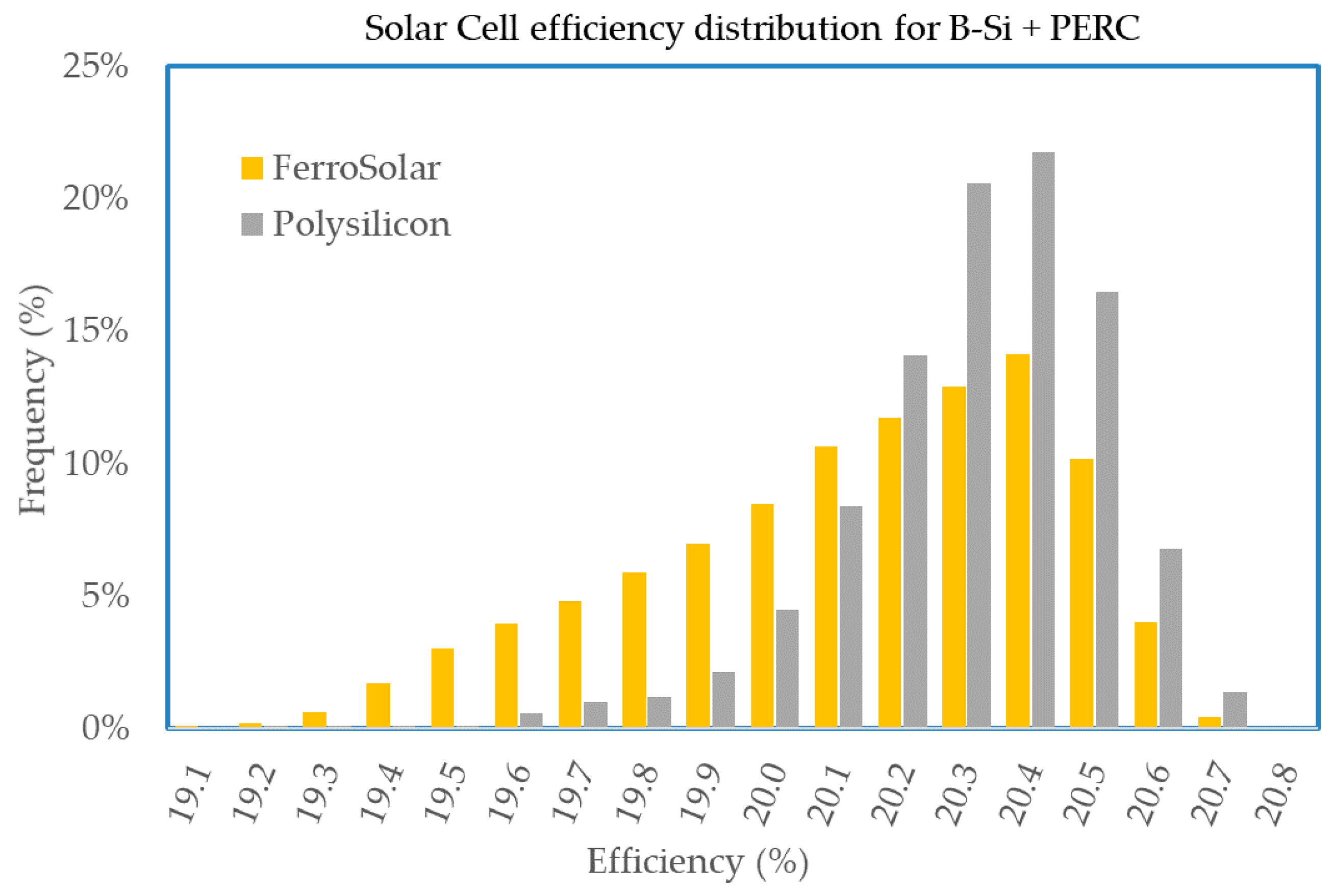
| B-Si (RIE) + PERC | UMG | 4.945 | 0.649 | 9.54 | 79.87 | 20.130 | 1.37% | 0.550 | 8.994 | 279 | 46,197 | TEST 3 Prod.B |
| Poly | 5.014 | 0.651 | 9.62 | 80.02 | 20.410 | --------- | -------- | 508 | 55,396 | |||
© 2019 by the authors. Licensee MDPI, Basel, Switzerland. This article is an open access article distributed under the terms and conditions of the Creative Commons Attribution (CC BY) license (http://creativecommons.org/licenses/by/4.0/).
Share and Cite
Forniés, E.; Ceccaroli, B.; Méndez, L.; Souto, A.; Pérez Vázquez, A.; Vlasenko, T.; Dieguez, J. Mass Production Test of Solar Cells and Modules Made of 100% UMG Silicon. 20.76% Record Efficiency. Energies 2019, 12, 1495. https://doi.org/10.3390/en12081495
Forniés E, Ceccaroli B, Méndez L, Souto A, Pérez Vázquez A, Vlasenko T, Dieguez J. Mass Production Test of Solar Cells and Modules Made of 100% UMG Silicon. 20.76% Record Efficiency. Energies. 2019; 12(8):1495. https://doi.org/10.3390/en12081495
Chicago/Turabian StyleForniés, Eduardo, Bruno Ceccaroli, Laura Méndez, Alejandro Souto, Antonio Pérez Vázquez, Timur Vlasenko, and Joaquín Dieguez. 2019. "Mass Production Test of Solar Cells and Modules Made of 100% UMG Silicon. 20.76% Record Efficiency" Energies 12, no. 8: 1495. https://doi.org/10.3390/en12081495