Flux-Balance Control for LLC Resonant Converters with Center-Tapped Transformers


Department of Electrical Engineering, National Taiwan University, Taipei, Taiwan; No. 1, Sec. 4, Roosevelt Rd., Taipei 10617, Taiwan
*
Author to whom correspondence should be addressed.
Energies 2019, 12(17), 3211; https://doi.org/10.3390/en12173211
Submission received: 9 July 2019
/
Revised: 18 August 2019
/
Accepted: 19 August 2019
/
Published: 21 August 2019
(This article belongs to the Special Issue Advances in High-Efficiency LLC Resonant Converters)
Abstract
:LLC resonant converters with center-tapped transformers are widely used. However, these converters suffer from a flux walking issue, which causes a larger output ripple and possible transformer saturation. In this paper, a flux-balance control strategy is proposed for resolving the flux walking issue. First, the DC magnetizing current generated due to the mismatched secondary-side leakage inductances, and its effects on the voltage gain are analyzed. From the analysis, the flux-balance control strategy, which is based on the original output-voltage control loop, is proposed. Since the DC magnetizing current is not easily measured, a current sensing strategy with a current estimator is proposed, which only requires one current sensor and is easy to estimate the DC magnetizing current. Finally, a simulation scheme and a hardware prototype with rated output power 200 W, input voltage 380 V, and output voltage 20 V is constructed for verification. The simulation and experimental results show that the proposed control strategy effectively reduces the DC magnetizing current and output voltage ripple at mismatched condition.
1. Introduction
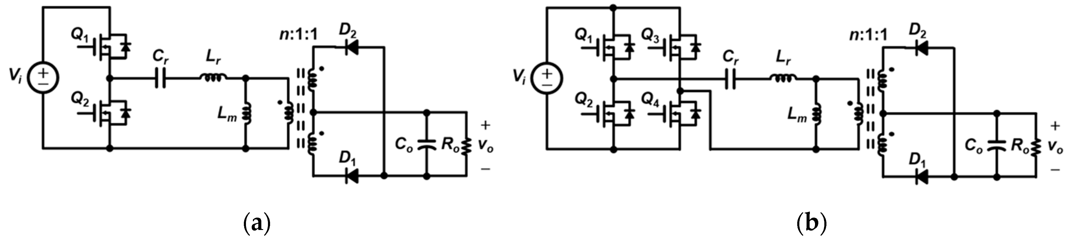
The LLC resonant converter is widely used in many different applications such as onboard chargers, server power systems, laptops, desktops, photovoltaic regeneration systems. Owing to the characteristics of zero-voltage-switching (ZVS) at the primary side and zero-current-switching (ZCS) at the secondary side, high efficiency and high power density of the LLC converter are achieved [1,2,3,4,5,6,7]. The half-bridge (HB) and full-bridge (FB) with the center-tapped transformer rectifier topologies shown in Figure 1 are the most commonly used topologies of the LLC resonant converter. Thanks to the center-tapped transformer, only two rectifying diodes are necessary at the secondary side [8,9,10,11]. Without the center-tap, it would be required to implement a full-wave rectifier.
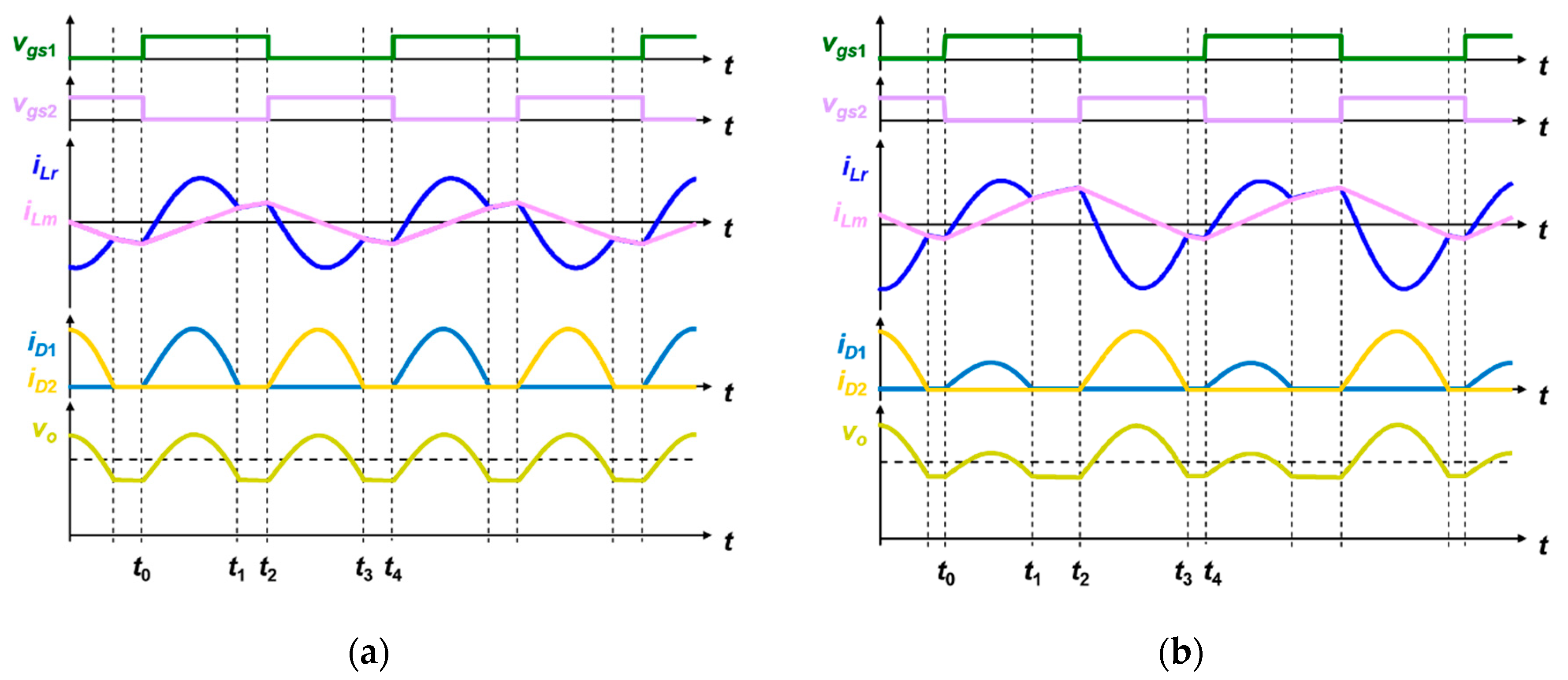
Figure 2a shows the key waveforms of the LLC resonant converter operating below the resonant frequency with the matching leakage inductances in both secondary side windings, where vgs1 and vgs2 are the driving signals of the MOSFET Q1 and Q2, respectively. Figure 2a reveals that the current waveforms of the diode 1 (iD1) and diode 2 (iD2) are symmetrical, and energy flows through the diode 1 and diode 2 in the positive and negative cycles, respectively. In Figure 2a, the magnetizing current will have no DC component.
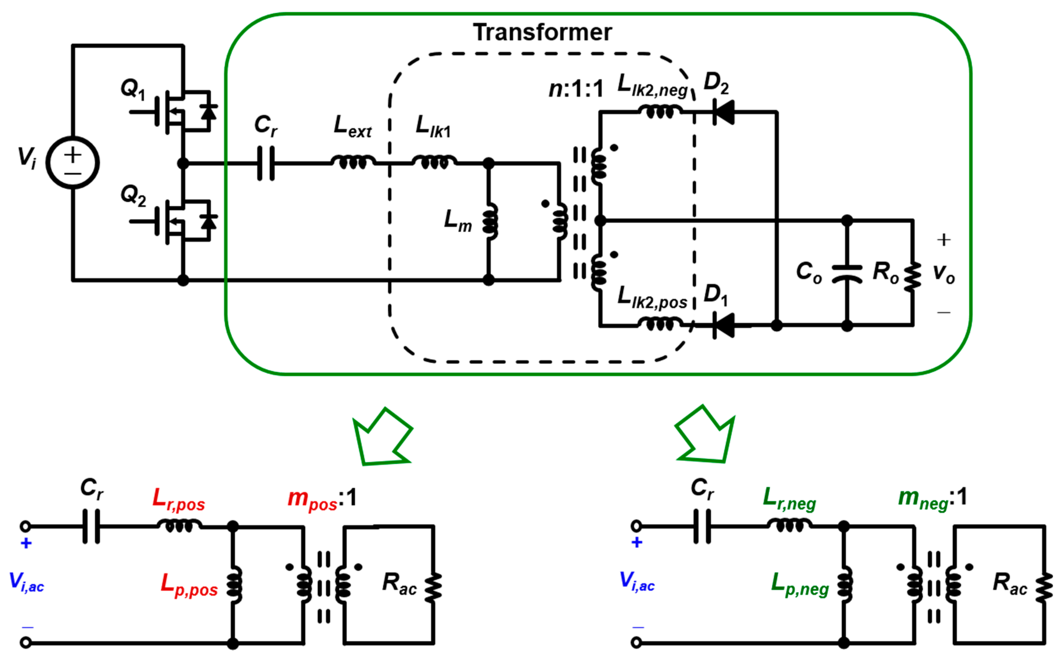
However, practical LLC resonant converters with center-tapped transformers contain a flux walking issue, which causes a larger output ripple and possible transformer saturation [12,13,14]. This is because the secondary side windings are usually not symmetrical in practical manufacture. The mismatched leakage inductances are generated in the secondary side windings, which causes an imbalance in the secondary side currents, resulting in a larger output voltage ripple. The secondary side currents imbalance will reflect upon the magnetizing inductance on the primary side. Therefore, the magnetizing current will have a DC component, which will lead to the flux walking and possible transformer core saturation.
Figure 2b shows the key waveforms of the LLC resonant converter operating below the resonant conditions with the mismatched leakage inductances in the secondary side windings. In Figure 2b, the current waveforms of the diode 1 and diode 2 are not symmetrical. The magnetizing current (iLm) will, therefore, contain a DC component. Since the resonant capacitance is in series with the primary side, the resonant current (iLr) will not have a DC component from charge balance concept. Besides, the mismatched condition considers not only the leakage inductances of the secondary side windings of the transformer but also the parasitic inductances of the printed-circuit-board (PCB) traces on the secondary side.
To improve the flux walking issue in the LLC resonant converter, improved winding structures for the secondary side were proposed [12,13,14]. The coupling coefficients between the primary side and two secondary sides were increased to mitigate the flux walking issue [12]. The further improved method is used in the Bifilar winding structure to overcome this problem [13]. The flux distribution of the non-symmetrical structure of the secondary side windings were analyzed in [14]. However, they cannot consider the mismatch problems caused by the PCB circuit traces.
According to abovementioned issue, a flux-balance control strategy, which is based on the original output-voltage control loop, is proposed in this paper. The flux-balance control is added to improve the magnetizing current imbalance problem caused by the secondary side mismatches.
Besides, the DC magnetizing current of the LLC resonant converter is difficult to sense directly. An indirect method to sense the magnetizing current was used [15], which involved sensing the currents at the primary and secondary side, simultaneously and subtracting them to obtain the magnetizing current. Then, the DC component was obtained using a low-pass filter. This solution, however, required several current sensing devices, which increased the circuit cost; moreover, the low-pass filter produced a slow dynamic response. Therefore, this paper proposes a simple magnetizing current sensing strategy with a DC current estimation scheme to overcome the abovementioned issue.
Moreover, for small-signal model, the mathematical methods for deriving the small-signal dynamic model of the LLC resonant converter were developed [16,17,18,19]. However, these works focused only on the switching frequency to output voltage transfer function. Besides, matching with circuit ac sweep simulation occurs only under specific operating conditions. Nevertheless, system identification [20,21] is a useful method to obtain the small-signal model of the system without using any complex mathematical model. Therefore, the system identification [21] is used to obtain the small-signal models of the LLC resonant converter for controllers design in this paper.
The remainder of this paper is organized as follows. Section 2 analyzes the mismatched leakage inductances effects of the secondary side on the DC magnetizing current and voltage gain. Section 3 describes the proposed control strategy with the magnetizing current sensing and the DC magnetizing current estimation. Section 4 describes the controller designs for the flux-balance loop and output-voltage loop, which are based on the transfer functions obtained by using the system identification tool of MATLAB (R2018b, MathWorks, Natick, MA, USA). Section 5 presents the simulated and experimental results, to verify the effectiveness of the proposed control strategy. Finally, Section 6 provides the conclusions.
2. Analysis of Secondary Side Mismatched Leakage Inductances Effects
2.1. Analysis of the Magnetizing Current DC Value
Figure 3 shows the DC current path in the LLC resonant tank when the leakage inductances at the secondary side are mismatched. It is assumed that the leakage inductance of the positive-cycle loop at the secondary side (Llk2,pos) is smaller than the leakage inductance of the negative-cycle loop at the secondary side (Llk2,neg). According to Kirchhoff’s current law (KCL), the relationship among iLr, iLm, and iDx can be expressed as follows
where n is the turns ratio of the transformer. Since the resonant capacitance is in series with the input of the transformer, the DC current of the resonant inductor is zero. That is, the average resonant inductor current in a switching period is zero in steady-state, and can be expressed as follows
Based on (3), the relationship between the magnetizing DC current and difference in the DC currents of both diodes can be expressed as follows
where ID1,DC and ID2,DC are the DC currents of the diodes at secondary side. Equation (4) shows that the magnetizing DC current is proportional to the difference between ID1,DC and ID2,DC with the turns ratio n. Therefore, the largest ILm,DC would be induced for the largest current mismatch in the secondary side condition.
2.2. Analysis of the Voltage Gain under Mismatched Condition
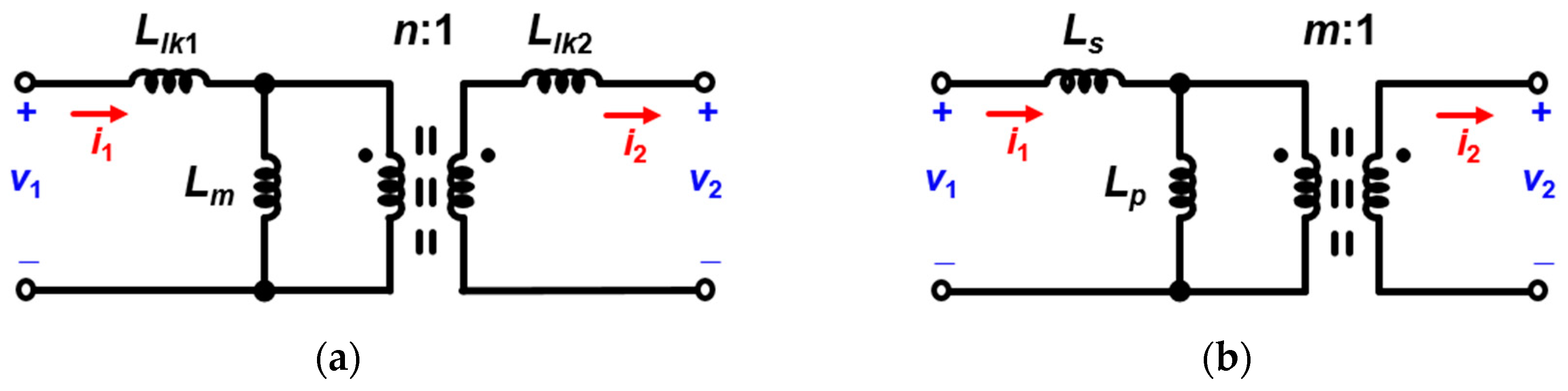
A non-ideal transformer equivalent circuit can be expressed by the model shown in Figure 4a, which is called the “T model” [22,23]. In Figure 4a, the leakage inductances are distributed at the primary and secondary sides, separately. This circuit is not suitable for the analysis of the LLC resonant converter. On the other hand, Figure 4b shows the “L model” [22,23]. In this model, the leakage inductance at the secondary side is removed. Therefore, it is suitably used in the LLC resonant tank for analysis.
For center-tapped applications, the L model of the transformer can be separated into the positive and negative cycle models. For a matched condition, the parameters of the L model for the positive and negative cycle will be the same. This will not be the case for the mismatched condition because the leakage inductances at the secondary side would affect the resonant parameters during the positive and negative cycles.
Figure 5 shows the equivalent circuit models of the LLC resonant tank for the positive (lower left) and negative (lower right) cycles. The relative parameters of the L model during the positive and negative cycles can be derived from Figure 4 and is presented as follows
where Lm indicates the magnetizing inductance of the transformer, Llk1 and Llk2,h express the leakage inductances at the primary and secondary sides of the transformer, respectively, mh indicates the equivalent turns ratio of the L model, Lext represents the external resonant inductance, Lp,h expresses the equivalent paralleled inductance of the L model, and Lr,h is the total equivalent resonant inductance of the L model. Therefore, the parameters of the L model during the positive and negative cycles can be obtained using (5)–(8).
The voltage gain during the positive and negative cycles can be expressed as follows
where fr indicates the resonant frequency, Cr is the resonant capacitance, Qh is the qualify factor, Rac is the equivalent ac load resistance, Ro is the load resistance, fs is the switching frequency, fn,h is the normalized frequency, and Ln,h is the ratio between Lp,h and Lr,h.
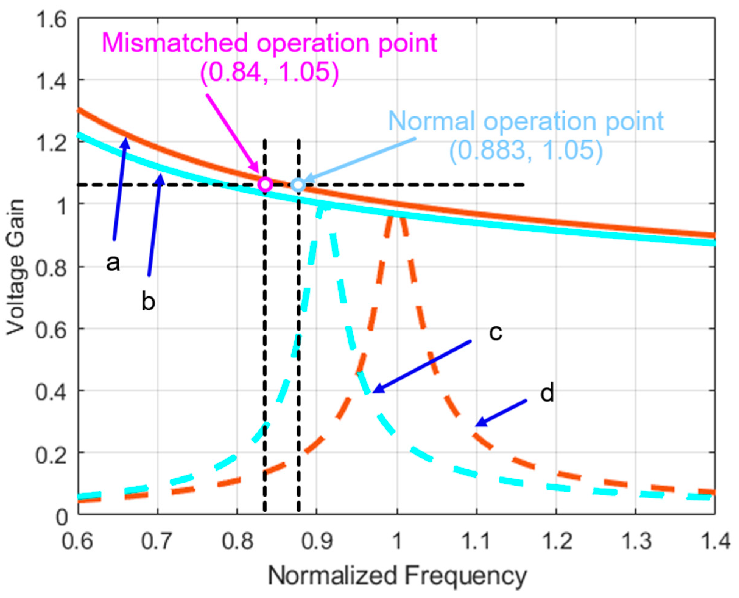
Based on (9)–(14), the voltage gain curves during the positive and negative cycles can be drawn as shown in Figure 6. The solid lines represent the nominal Q-value condition and dashed lines express the high Q-value condition. Assuming the normal leakage inductance Llk,2n = Llk,2,pos = Llk,2,neg at the secondary side, i.e., at matched condition, fn,pos and fn,neg would be one as indicated by the curve a (i.e., maroon solid line) with the normal operating point indicated by the sky blue circle in Figure 6. When operating under the mismatched condition and assuming the leakage inductances at the secondary side are satisfying Llk,2n = Llk,2,pos < Llk,2,neg, the voltage gain during the positive cycle follows the original curve a (i.e., maroon solid line); during the negative cycle, the voltage gain curve moves toward the left as shown by the curve b (i.e., light blue solid line). Under the mismatched condition, the voltage gain also operates at M = 1.05, because of the voltage loop regulation, and the operating point shifts to the point indicated by the pink circle.
The operations of the curve a (i.e., maroon solid line) during the positive cycle and curve b (i.e., light blue solid line) during the negative cycle can be mapped to time-domain operated waveforms shown in Figure 2b. They are matched precisely between the voltage gains and time domain waveforms.
3. Proposed Flux-Balance Control Architecture
3.1. Description of the Proposed Control Architecture
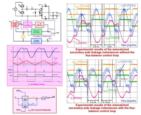
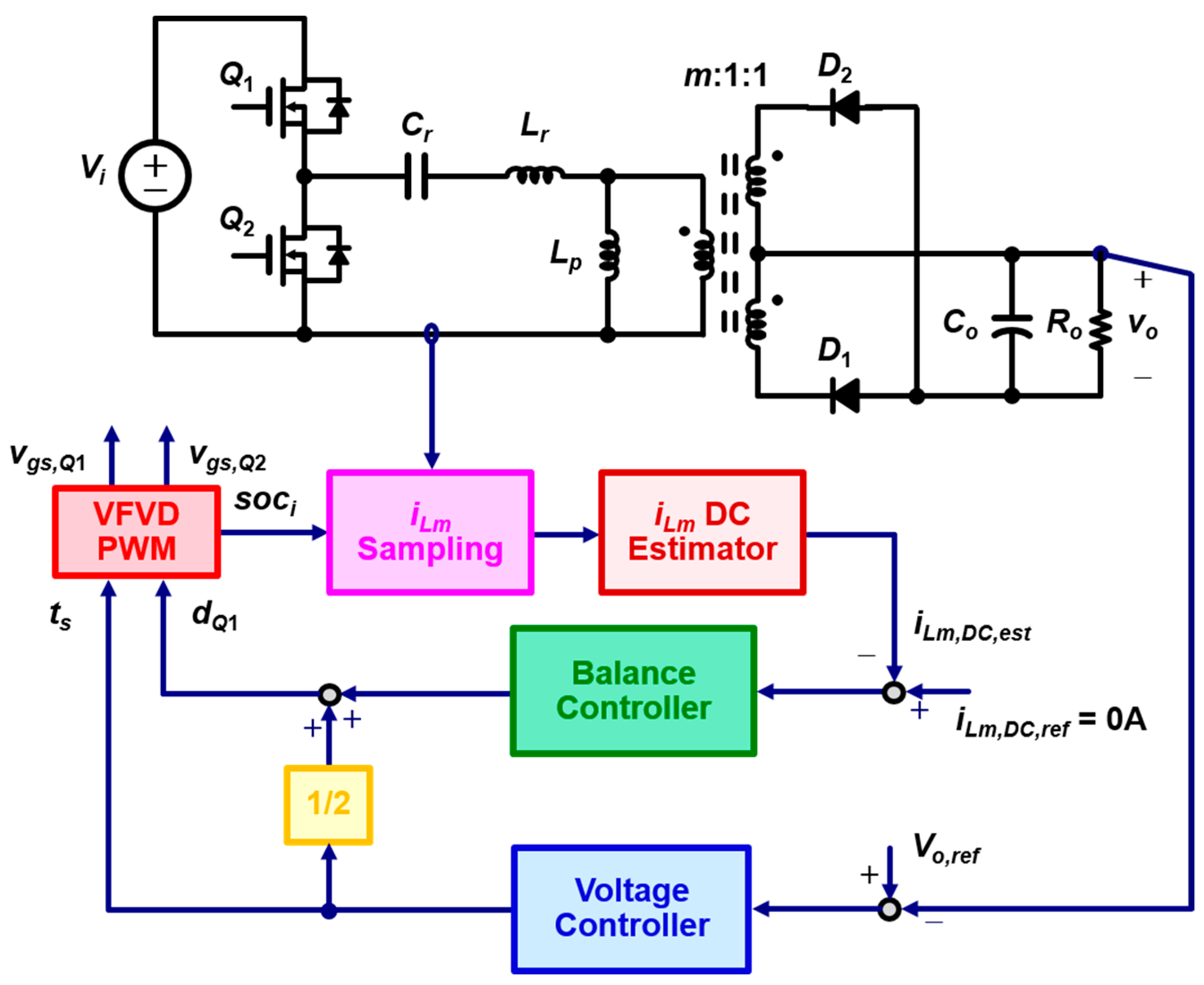
Figure 7 shows the block diagram of the proposed control architecture to solve the flux walking issue caused by the mismatched condition on the secondary side. The proposed control is based on the original output-voltage control loop with the addition of the flux-balance loop. The flux-balance loop includes the sampling setup for the magnetizing current, a DC current estimator, a flux-balance loop controller, and a variable-frequency-variable-duty-pulse-width-modulator (VFVDPWM). The output of the voltage loop controller controls the switching period of the MOSFETs Q1 and Q2. The output of the flux-balance loop controller offsets the duty ratio of the MOSFETs Q1 and Q2 from 0.5. The input of the flux-balance loop controller is the error between iLm,DC and iLm,DC,ref, which is zero in steady-state. Thus, the flux-balance loop forces the DC magnetizing current to zero and solves the flux walking issue. The DC estimator estimates the DC magnetizing current, and the iLm sampling scheme samples relative information of the magnetizing current from the resonant current iLr. The relationship between the DC magnetizing current and the duty ratio are not direct, because the resonant capacitance is in series between the half-bridge switches and the input of the transformer. According to the proposed flux-balance control, when the duty is regulated, the resonant capacitance to hold the charge balance in steady-state, the DC current of the resonant inductance, therefore, keeps zero, and the rectifier diodes turned off time, therefore, be changed when the duty ratio be regulated. Finally, the magnetizing DC current would be regulated. Detailed descriptions of the functional blocks of the magnetizing current sampling scheme, the DC current estimator, and the VFVDPWM are provided below.
3.2. Magnetizing Current Sampling Scheme
Figure 8 shows the magnetizing current sampling scheme, where iLr is the resonant current, iLm is the magnetizing current, iLm,p, and iLm,n are the peak values of the magnetizing current during the positive and negative cycles, respectively. The magnetizing current of the LLC resonant converter cannot be measured directly because the magnetizing inductance is an equivalent element in the transformer. However, owing to the LLC resonant converter usually operates with the switching frequency below the resonant frequency, the resonant current is equal to the magnetizing current when the diodes on the secondary side are turned off. As shown in Figure 8, during these intervals, the peak values of the magnetizing current during the positive and negative cycles occur when the respective MOSFET Q1 and Q2, are turned off. According to the previous statement, the sampling pluses of SOCi,p and SOCi,n can be applied from the VFVDPWM, which are generated when the driving signals of MOSFET Q1 and Q2 are turned off, respectively. After that, iLm,p and iLm,n can be sampled during each switching period.
3.3. DC Value Estimation of the Magnetizing Current
This paper proposes the DC value estimation scheme to obtain the DC magnetizing current, which will be used as one of the inputs of the flux-balance controller. Figure 9 shows the magnetizing current waveform (red line), which is similar to a triangular wave (shown by the blue dashed line). The magnetizing DC current can be estimated after the iLm,p and iLm,n are sampled, and is expressed as follows
where iLm,DC,est[n] represents the estimated magnetizing DC current. Equation (15) reveals that the estimated magnetizing DC current can be approximated as the sum of iLm,p[n] and iLm,n[n], divided by 2, which is a very simple method to obtain the magnetizing DC current. The block diagram of the DC magnetizing current estimator is shown in Figure 10.
3.4. Variable-Frequency-Variable-Duty-Pulse-Width-Modulator
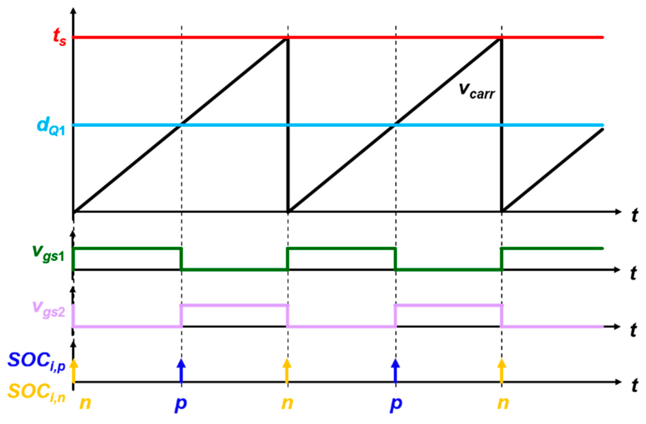
In conventional LLC resonant converters, the output voltage regulation is achieved by controlling the switching frequency and maintaining the duty ratios of MOSFET Q1 and Q2 at 50%. The proposed flux-balance control scheme utilizes the controlled duty ratio for MOSFET Q1 for the magnetizing DC current regulation. Figure 11 shows the operating timing of the VFVDPWM, where vcarr is the carrier waveform, dQ1 is the duty ratio control signal of MOSFET Q1, ts is the switching period control signal. In Figure 11, the slope of vcarr is fixed. ts can therefore control the magnitude of vcarr to control the switching period. dQ1, which is equal to 0.5ts in the matched condition, controls the duty ratio of MOSFET Q1 for the flux-balance loop regulation. SOCi,p is generated when dQ1 equals vcarr and SOCi,n is generated when ts equals vcarr. Thus, the control signal and magnetizing current sampling pulses of the proposed flux-balance loop can be obtained from Figure 11.
4. Small-Signal Model and Controllers Design
4.1. Small-Signal Models Built Using System Identification
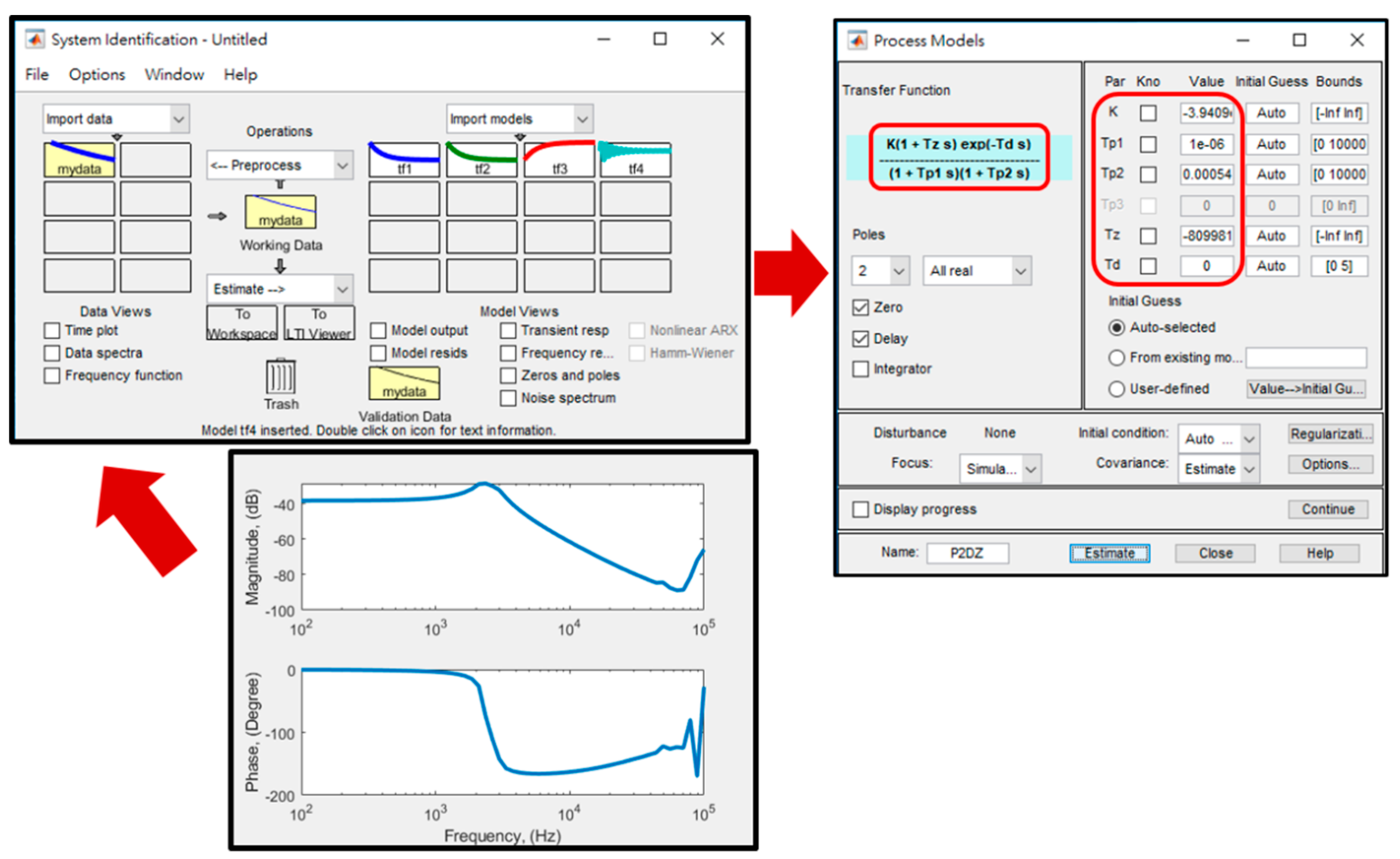
Unlike the pulse-width-modulation (PWM) converter, the LLC resonant converter is a complex nonlinear system. Therefore, it is difficult to obtain its small-signal model through mathematical derivation. Previously, researchers had developed the mathematical methods for deriving the small-signal dynamic model of the LLC resonant converter [16,17,18,19]. However, these works focused only on the matching with circuit ac sweep simulation occurs only under specific operating conditions. At the same time, the flux-balance loop proposed in this paper, there is no more literature to discuss. The system identification tool of MATLAB [21] is a useful tool to obtain the small-signal model transfer function without using any complex mathematical model derivation. Figure 12 shows the processing flow windows of the system identification of MATLAB. The transfer function of the system can be obtained from the simulated or measured system data such as time response or frequency response. Therefore, the system identification tool of MATLAB [21] is used to obtain the small-signal model for controller design, in this paper.
4.2. Flux-Balance Loop Controller Design
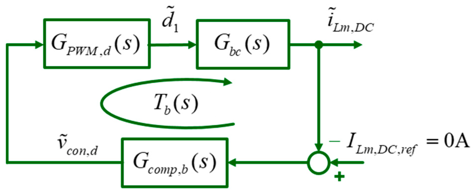
Figure 13 shows the control block diagram of the flux-balance loop, for which the loop gain can be expressed as
where Gbc(s) represents the transfer function of the controlled plant, which is the duty ratio of MOSFET Q1 (d1-tilde) to the magnetizing DC current (iLm,DC-tilde), GPWM,d(s) represents the transfer function of the duty ratio control signal (vcon,d-tilde) to the duty ratio of MOSFET Q1, and Gcomp,b(s) indicates the controller of the flux-balance loop.
Using the system identification tool of MATLAB, the uncompensated loop gain from the duty ratio control signal to the magnetizing DC current under full load operation condition can be expressed as follows. The parameters of the LLC resonant converter are shown in Table 1, which will be shown in Section 5.
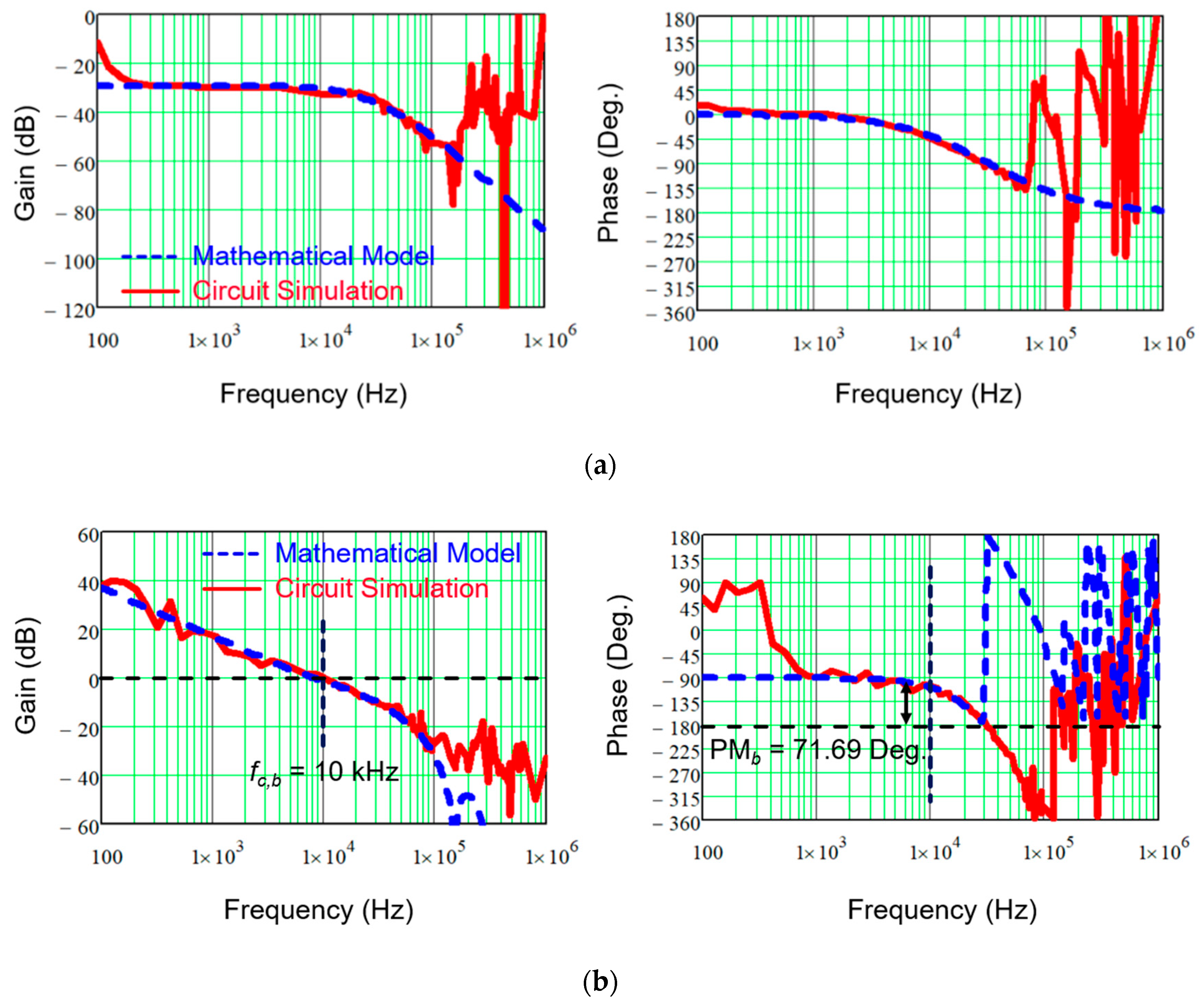
The characteristic equation in (17) has two real poles at 110 krad/s (17.5 kHz) and 377 krad/s (60 kHz), respectively. Figure 14a shows the bode plots of the uncompensated flux-balance loop gains obtained from the mathematical model in (17) (blue dashed line) and Simplis circuit simulation (red solid line). Figure 14a reveals that the dominate pole is at 17.5 kHz. The controller of the flux-balance loop Gcomp,b(s) can, therefore, be chosen as a PI-type controller and can be expressed as follows
where Kpb is the DC gain, which is determined according to the crossover frequency sets as fc,b = 10 kHz, and zb is the zero, which is set at 17.5 kHz for pole/zero cancellation. The phase margin (PM) is set as 72° to ensure stability. The bode plot of the compensated flux-balance loop gain, after the addition of the controller, is shown in Figure 14b.
4.3. Output-Voltage Loop Controller Design
Figure 15 shows the control block diagram of the output-voltage loop, the loop gain of which can be expressed as follows
where Gfv(s) represents the transfer function of the controlled plant, which is the switching frequency of MOSFET Q1 (f-tilde) to the output voltage (vo-tilde), GPWM,d(s) represents the transfer function of the switching frequency control signal (vcon,f-tilde) to the switching frequency of MOSFET Q1, and Gcomp,v(s) is the controller of the output-voltage loop.
Using the system identification tool of MATLAB, the uncompensated loop gain from the switching frequency control signal to the output voltage under full load operation condition can be expressed as follows. The parameters of the LLC resonant converter are shown in Table 1.
The characteristic equation in (20) has a complex pole pair at 21.42 ± j18.346 krad/s (3.41 ± j2.9 kHz) and a zero at 30.97 krad/s (4.93 kHz). Figure 16a shows the bode plots of the uncompensated output-voltage loop gains obtained from the mathematical model in (20) (blue dashed line) and Simplis circuit simulation (red solid line). Figure 16a reveals that the phase down to −90°, due to the zero, is very close to complex pole pair. Thus, (20) can be simplified as a first-order system. The controller of the output voltage Gcomp,v(s) can also be chosen as a PI-type controller and can be expressed as follows
where Kpv is the DC gain, which is determined according to the crossover frequency sets as fc,v = 6 kHz, zv is the zero, which is set at 18.85 kHz for pole/zero cancellation, and the phase margin at fc,v is 78.33° to ensure stability. The bode plot of the compensated output-voltage loop gain, after the addition of the controller, is shown in Figure 16b.
5. Simulation and Experimental Verification
To verify the proposed approach, Simplis software was used to construct the simulation, and an experimental platform was built as shown in Figure 17. In this paper, the center-tapped model constructed in Simplis is similar to Figure 5. Two ideal transformers, where the primary side is connecting in parallel, and the secondary side connecting in series, are used. The magnetizing inductance and leakage inductances are added in the primary side and secondary sides, respectively. The advantage of this method is that all of branches current and nodes voltages can easily be measured for observation and analysis.
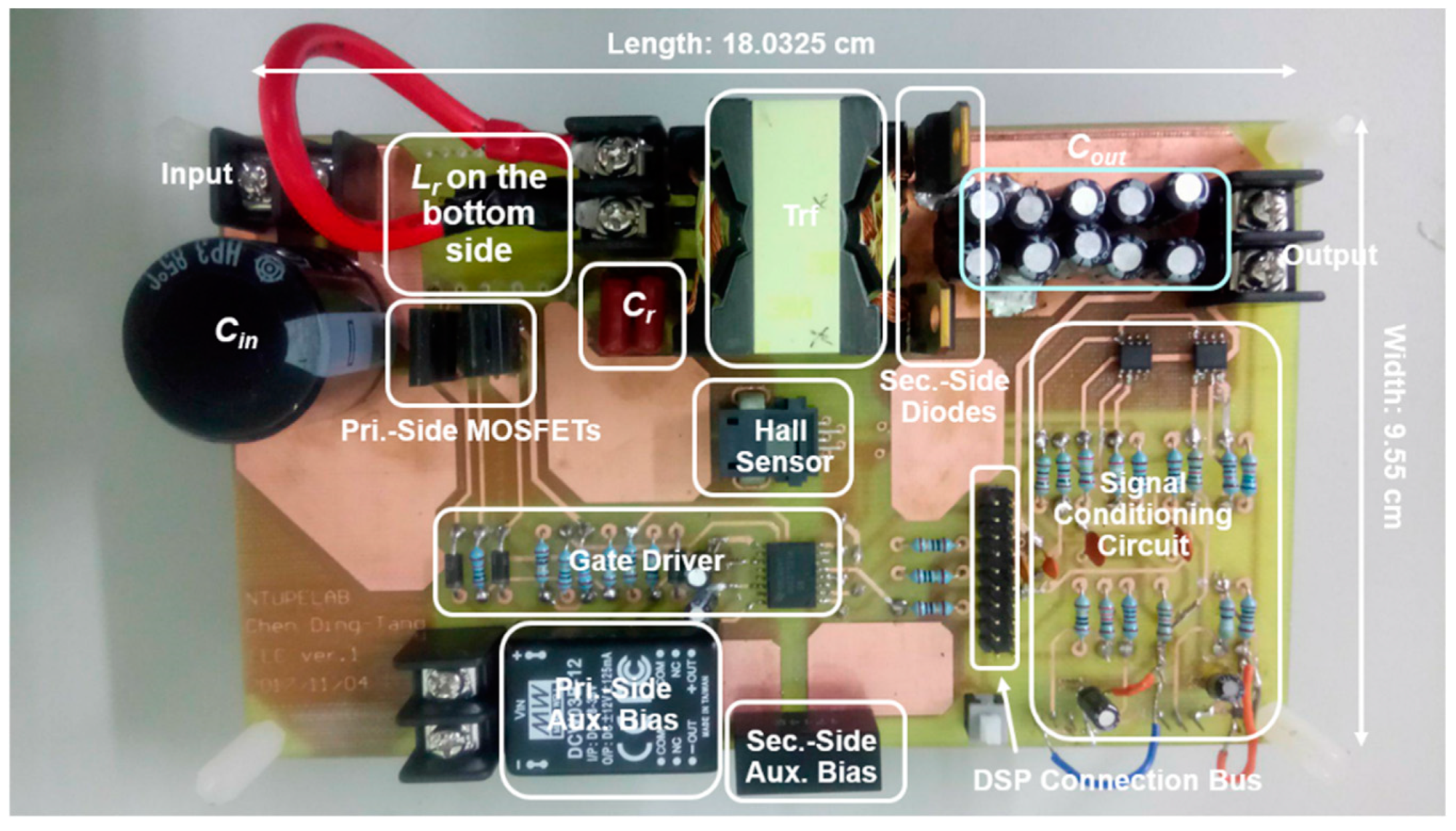
The proposed flux-balance control strategy was implemented by using Texas Instrument C2000 Piccolo 28035 digital signal processor. For experimental equipment, Agilent Technologies InfiniiVision DSO-X 3054A oscilloscope (BW = 500 MHz) was used; Keysight Technologies 1147B current probe (BW = 50 MHz) was used for iLr measurement, and Sapphire Instrument LDP-6002 (BW = 25 MHz) differential voltage probes were used for differential voltage measurement (vgs1). Table 1 lists the related parameters of the LLC resonant converter. The leakage inductance at the secondary side, during the negative cycle, covers the matched condition (Llk2,neg = 53 nH) and mismatched condition (Llk2,neg = 167.77 nH). The set switching frequency is less than the resonant frequency, i.e., fs < fr, for an input voltage Vi = 380 V.
5.1. Steady-State Operation
Figure 18 shows the simulated and experimental results of the LLC resonant converter at full load in steady-state operation with the matched secondary-side leakage inductances, i.e., Llk2,pos = Llk2,neg = 53 nH. In Figure 18a, the peak-to-peak ripple of the output voltage is approximately 734 mV. The conduction times of the secondary side diodes are 2.96 μs. The resonant frequency is fr = 168.9 kHz, and switching frequency is fs = 134.78 kHz. In Figure 18b, the peak-to-peak ripple of the output voltage is 700 mV and conduction times of the secondary-side diodes are approximately 3.14 μs during the positive and negative cycles. Therefore, the resonant frequency is fr = 159.23 kHz and switching frequency is fs = 130.11 kHz. The simulated and experimental results show that the magnetizing current is almost balanced between horizontal axis, i.e., ILm,DC = 0 A, but some parasitic effects in the secondary side of the hardware cause a mismatch between the simulated and experimental results.
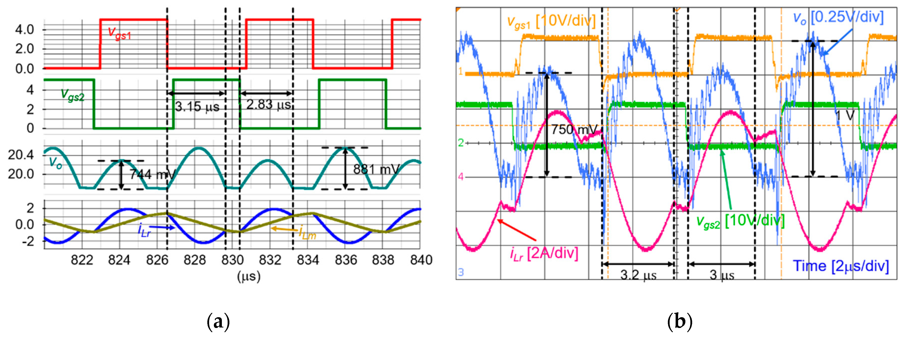
Figure 19 shows the simulated and experimental results of the LLC resonant converter at steady-state, when operating at full load with the mismatched secondary side leakage inductances, i.e., Llk2,pos = 53 nH and Llk2,neg = 167.77 nH. In Figure 19a, the peak-to-peak ripples of the output voltage during the positive and negative cycles are 744 mV and 881 mV, respectively. The conduction time of the secondary side diode during the positive cycle is 2.83 μs. Therefore, the resonant frequency during the positive cycle is fr,pos = 176.67 kHz. The conduction time of the secondary side diode during the negative cycle is 3.15 μs. Hence, the resonant frequency during the negative cycle is fr,neg = 158.73 kHz. The switching frequency is fs = 127.98 kHz and magnetizing DC current is ILm,DC = 436 mA. In Figure 19b, the peak-to-peak ripples of the output voltage during the positive and negative cycles are 750 mV and 1 V, respectively. The conduction time of the secondary side diode during the positive cycle is 3 μs. Hence, the resonant frequency during positive cycle is fr,pos = 166.67 kHz. The conduction time of the secondary side diode during the negative cycle is 3.2 μs; therefore, the resonant frequency during the negative cycle is fr,neg = 156.25 kHz. The switching frequency is fs = 127.01 kHz. The magnetizing DC current can be estimated as ILm,DC,est = 400 mA using (15), which is approximately the same as the simulated result, although the experimental result does not measure the magnetizing DC current directly.
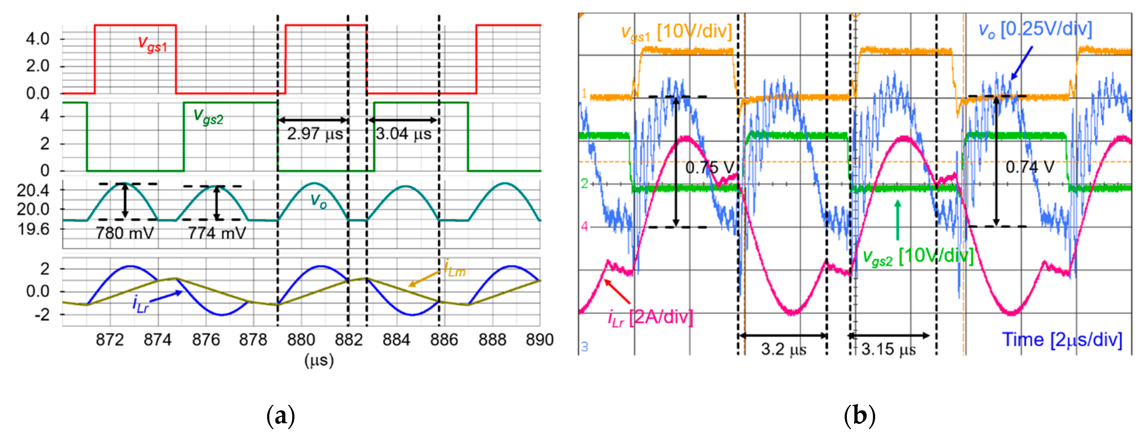
Figure 20 shows the simulated and experimental results of the LLC resonant converter at full load in steady-state with the flux-balance loop control, for the same mismatched condition as that in Figure 19. In Figure 20a, the peak-to-peak ripples of the output voltage during the positive and negative cycles are 780 mV and 774 mV, respectively. The conduction time of the secondary side diode during the positive cycle is 2.97 μs; therefore, the resonant frequency during positive cycle is fr,pos = 168.35 kHz. The conduction time of the secondary side diode during the negative cycle is 3.04 μs; hence, the resonant frequency during the negative cycle is fr,neg = 164.47 kHz. The switching frequency is fs = 125.37 kHz and magnetizing DC current is ILm,DC = 19 mA. In Figure 20b, the peak-to-peak ripples of the output voltage during the positive and negative cycles are 750 mV and 740 mV, respectively. The conduction time of the secondary side diode during the positive cycle is 3.15 μs; hence, the resonant frequency during positive cycle is fr,pos = 158.73 kHz. The conduction time of the secondary side diode during the negative cycle is 3.2 μs; therefore, the resonant frequency during negative cycle is fr,neg = 156.25 kHz. The switching frequency is fs = 126.21 kHz. The magnetizing DC current can be estimated to be ILm,DC,est = 20 mA, using (15). The magnetizing DC current estimated from the experimental result is close to the value obtained from the simulations, which confirms the effectiveness of the approach proposed in this paper.
5.2. Dynamic-State Operation
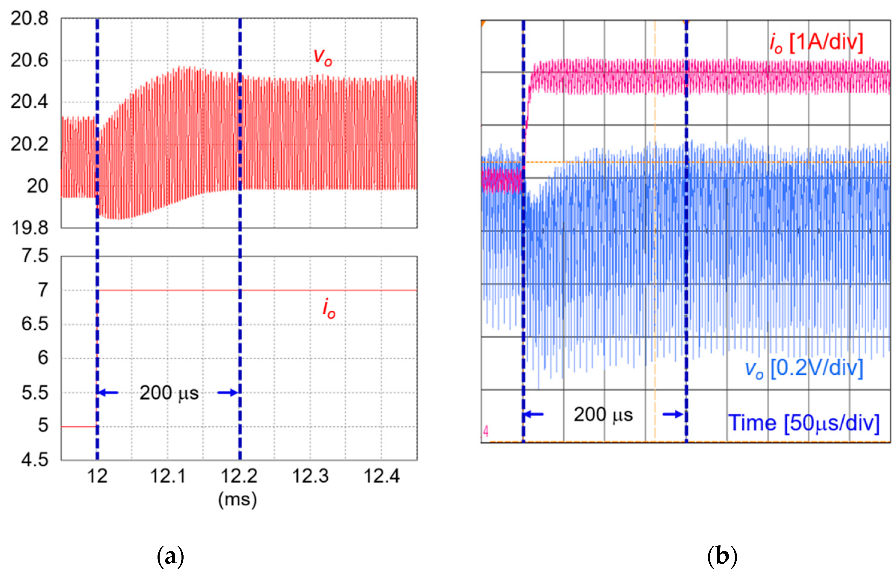
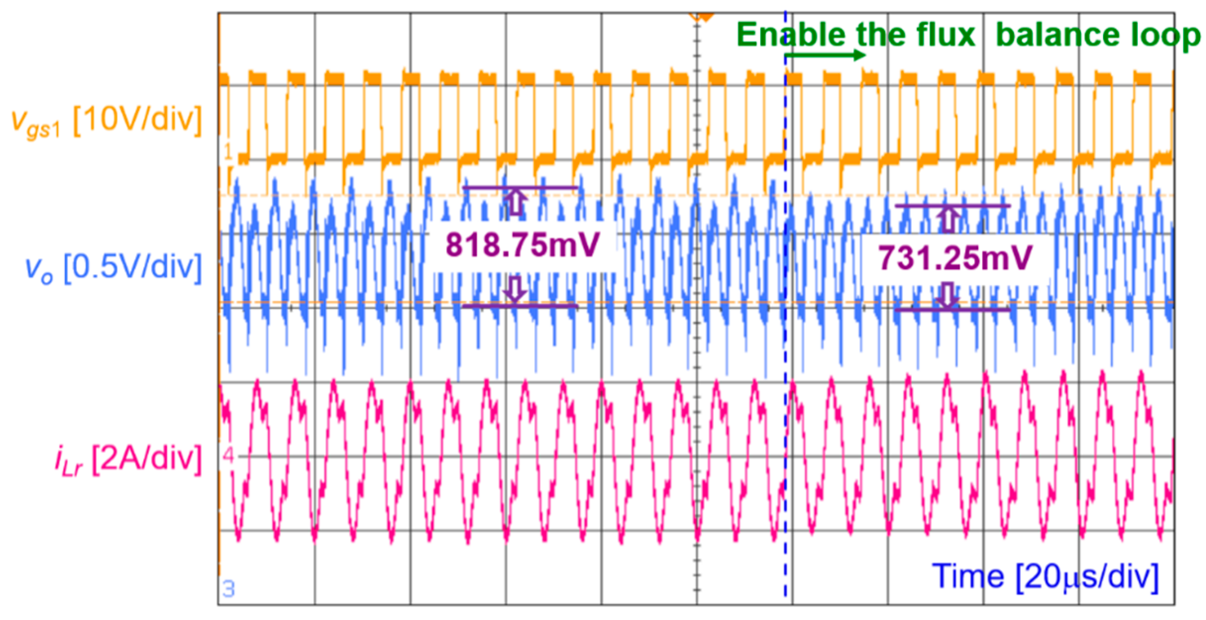
Figure 21 shows the simulated and experimental results of the transient response of the LLC resonant converter, which compensates for the mismatched secondary side leakage inductances using the flux-balance loop, for load changes from 50% to 70%. The transient time is approximately 200 μs, as shown in the simulated and experimental results. Figure 21 reveals that the voltage loop and the flux-balance loop operate simultaneously, without affecting each other in the transient state. Figure 22 shows the simulated and experimental results of the transient response of the LLC resonant converter, which compensates for the mismatched secondary side leakage inductances with the flux-balance loop, for load changes from 70% to 50%. The simulated and experimental results show that the transient time is 200 μs. Figure 22 shows that the voltage loop and flux-balance loop do not affect each other, even during the load step down. Figure 23 shows the experimental results of the disabled and enabled flux-balance loop at 70% load, considering the mismatched secondary side leakage inductances. When the flux-balance loop is disabled, the maximum peak-to-peak ripple of the output voltage is 818.75 mV. Once the flux-balance loop is enabled, the maximum peak-to-peak ripple of the output voltage reduces to 731.25 mV.
6. Conclusions
In this paper, a flux-balance loop control strategy was proposed to solve the flux walking issues of the center-tapped transformer in the LLC resonant converter, which were caused by mismatched leakage inductances at the secondary side. The magnetizing DC current effect and voltage gain parameter variation caused by the mismatched conditions at the secondary side were analyzed. Based on these analyses, the flux-balance control loop combining with the original output-voltage control loop, was proposed to resolve the issues. Besides, a magnetizing DC current sampling strategy and estimation scheme was also proposed to overcome the difficulties in measuring the magnetizing DC current. The simulation and experimental results confirmed the effectiveness of the proposed control strategy.
Author Contributions
Y.-C.L. substantially contributed to literature search, control strategy design, examination and interpretation of the results, development of the overall system, and review and proofreading of the manuscript. D.-T.C. substantially contributed to implement the control strategy, production and analysis of the results, and preparation and revision of the manuscript. C.-J.C. substantially contributed to the review and proofreading of the manuscript.
Funding
This work was supported by the Ministry of Science and Technology (MOST) in Taiwan under grants MOST 107-2221-E-002-054-MY2 and National Taiwan University under grants NTU-CC-108L890701.
Acknowledgments
The authors want to thank SIMPLIS Technologies Corporation, U.S.A, for providing SIMPLIS simulation tool.
Conflicts of Interest
The authors declare no conflict of interest.
References
- Deng, J.; Li, S.; Hu, S.; Mi, C.; Ma, R. Design methodology of LLC resonant converters for electric vehicle battery chargers. IEEE Trans. Veh. Technol. 2014, 63, 1581–1592. [Google Scholar] [CrossRef]
- Shen, Y.; Zhao, W.; Chen, Z.; Ca, C. Full-bridge LLC resonant converter with series-parallel connected transformers for electric vehicle on-board charger. IEEE Access 2018, 6, 13490–13500. [Google Scholar] [CrossRef]
- Amirahmadi, A.; Domb, M.; Persson, E. High power density high efficiency wide input voltage range LLC resonant converter utilizing E-mode GaN switches. In Proceedings of the 2017 IEEE Applied Power Electronics Conference and Exposition (APEC), Tampa, FL, USA, 26–30 March 2017; pp. 350–354. [Google Scholar]
- Joung, M.; Kim, H.; Baek, J. Dynamic analysis and optimal design of high efficiency full bridge LLC resonant converter for server power system. In Proceedings of the 2012 27th Annual IEEE Applied Power Electronics Conference and Exposition (APEC202), Orlando, FL, USA, 5–9 February 2012; pp. 1292–1297. [Google Scholar]
- Kim, B.-C.; Park, K.-B.; Kim, C.-E.; Lee, B.-H.; Moon, G.-W. LLC resonant converter with adaptive link-voltage variation for a high-power-density adapter. IEEE Trans. Power Electron. 2010, 25, 2248–2252. [Google Scholar] [CrossRef]
- Hu, S.; Deng, J.; Mi, C.; Zhang, M. LLC resonant converters for PHEV battery chargers. In Proceedings of the 2013 Twenty-Eighth Annual IEEE Applied Power Electronics Conference and Exposition (APEC2013), Long Beach, CA, USA, 17–21 March 2013; pp. 3051–3054. [Google Scholar]
- Wu, H.; Mu, T.; Gao, X.; Xing, Y. A secondary-side phase-shift-controlled LLC resonant converter with reduced conduction loss at normal operation for hold-up time compensation application. IEEE Trans. Power Electron. 2015, 30, 5352–5357. [Google Scholar] [CrossRef]
- D’Cruz, R.; Rajesh, M. Half bridge LLC resonant DC-DC converter for solar array simulator application. In Proceedings of the 2015 International Conference on Technological Advancements in Power and Energy (TAP Energy), Kollam, India, 24–26 June 2015; pp. 138–143. [Google Scholar]
- Yang, Y.-R. A half-bridge LLC resonant converter with loose-coupling transformer and transition capacitor. In Proceedings of the 2014 9th IEEE Conference on Industrial Electronics and Applications, Hangzhou, China, 9–11 June 2014; pp. 1344–1349. [Google Scholar]
- Huang, Y.-C.; Hsieh, Y.-C.; Lin, Y.-C.; Chiu, H.-R.; Lin, J.-Y. Study and implementation on start-up control of full-bridge LLC resonant converter. In Proceedings of the 2018 IEEE Transportation Electrification Conference and Expo, Asia-Pacific (ITEC Asia-Pacific), Bangkok, Thailand, 6–9 June 2018. [Google Scholar]
- Lin, R.-L.; Lin, C.-W. Design criteria for resonant tank of LLC DC-DC resonant converter. In Proceedings of the 36th Annual Conference on IEEE Industrial Electronics Society (IECON2010), Glendale, AZ, USA, 7–10 November 2010; pp. 427–432. [Google Scholar]
- Sato, M.; Nagaoka, S.; Uematsu, T.; Zaitsu, T. Mechanism of current imbalance in LLC resonant converter with center tapped transformer. In Proceedings of the 2018 International Power Electronics Conference (IPEC-Niigata 2018-ECCE Asia), Niigata, Japan, 20–24 May 2018; pp. 118–122. [Google Scholar]
- Jung, J.-H. Bifilar winding of a center-tapped transformer including integrated resonant inductance for LLC resonant converters. IEEE Trans. Power Electron. 2013, 28, 615–620. [Google Scholar] [CrossRef]
- Li, M.; Chen, Q.; Ren, X.; Zhang, Y.; Jin, K.; Chen, B. The integrated LLC resonant converter using center-tapped transformer for on-board EV charger. In Proceedings of the 2015 IEEE Energy Conversion Congress and Exposition (ECCE2015), Montreal, QC, Canada, 20–24 September 2015; pp. 6293–6298. [Google Scholar]
- Panov, Y.; Jovanović, M.; Irving, B. Novel transformer-flux-balancing control of dual-active-bridge bidirectional converters. In Proceedings of the 2015 IEEE Applied Power Electronics Conference and Exposition (APEC2015), Charlotte, NC, USA, 15–19 March 2015; pp. 42–49. [Google Scholar]
- Murakami, Y.; Sato, T.; Nishijima, K.; Nabeshima, T. Small signal analysis of LLC current resonant converters using equivalent source model. In Proceedings of the 42nd Annual Conference of the IEEE Industrial Electronics Society (IECON2016), Florence, Italy, 23–26 October 2016; pp. 1417–1422. [Google Scholar]
- Tian, S.; Lee, F.; Li, Q. A simplified equivalent circuit model of series resonant converter. IEEE Trans. Power Electron. 2016, 31, 3922–3931. [Google Scholar] [CrossRef]
- Tian, S.; Lee, F.; Li, Q. Equivalent circuit modeling of LLC resonant converter. In Proceedings of the 2016 IEEE Applied Power Electronics Conference and Exposition (APEC2016), Long Beach, CA, USA, 20–24 March 2016; pp. 1608–1615. [Google Scholar]
- Fang, Z.; Wang, J.; Duan, S.; Xiao, L.; Hu, G.; Liu, Q. Rectifier current control for an LLC resonant converter based on a simplified linearized model. Energies 2018, 11, 579. [Google Scholar] [CrossRef]
- MATLAB. System Identification Overview. Available online: https://www.mathworks.com/help/ident/gs/about-system-identification.html (accessed on 30 May 2019).
- MATLAB. System Identification Toolbox. Available online: https://www.mathworks.com/products/sysid.html (accessed on 30 May 2019).
- Simone, S.; Adragna, C.; Spini, C. Design guideline for magnetic integration in LLC resonant converters. In Proceedings of the 2008 International Symposium on Power Electronics, Electrical Drives, Automation and Motion (SPEEDAM2008), Ischia, Italy, 11−13 June 2008; pp. 950–957. [Google Scholar]
- Huang, H. FHA-based voltage gain function with harmonic compensation for LLC resonant converter. In Proceedings of the 25th Annual IEEE Applied Power Electronics Conference and Exposition (APEC2010), Palm Springs, CA, USA, 21−25 February 2010; pp. 1770–1777. [Google Scholar]
Figure 1.
Different topologies of the LLC resonant converter (a) half-bridge and (b) full-bridge.

Figure 2.
Key waveforms of the LLC resonant converter operating below the resonant frequency with the different leakage inductances in the secondary side windings (a) matched leakage inductances and (b) mismatched leakage inductances.
Figure 2.
Key waveforms of the LLC resonant converter operating below the resonant frequency with the different leakage inductances in the secondary side windings (a) matched leakage inductances and (b) mismatched leakage inductances.

Figure 3.
The DC current path in the LLC resonant tank when the leakage inductances at the secondary side are mismatched (Llk2,pos < Llk2,neg).
Figure 3.
The DC current path in the LLC resonant tank when the leakage inductances at the secondary side are mismatched (Llk2,pos < Llk2,neg).

Figure 4.
Different equivalent circuit models of the transformer (a) T model and (b) L model.

Figure 5.
Equivalent circuit models of the resonant tank during the positive cycle (lower left) and negative cycle (lower right).
Figure 5.
Equivalent circuit models of the resonant tank during the positive cycle (lower left) and negative cycle (lower right).

Figure 6.
Voltage gain curves during the positive and negative cycles, curve a: Nominal Q-value condition with the matched leakage inductance Llk,2n at the secondary side; curve b: Nominal Q-value condition with the mismatched leakage inductance Llk,2,neg at the secondary side during the negative cycle; curve c: High Q-value condition with the matched leakage inductance Llk,2n at the secondary side; curve d: High Q-value condition with the mismatched leakage inductance Llk,2,neg at the secondary side during the negative cycle.

Figure 7.
Overall block diagram of the proposed control architecture.

Figure 8.
Magnetizing current sampling timing, where iLm,p (iLm,n) is sampled at the timing of vgs1 (vgs2) from high to low.
Figure 8.
Magnetizing current sampling timing, where iLm,p (iLm,n) is sampled at the timing of vgs1 (vgs2) from high to low.

Figure 9.
The magnetizing current waveform (red line) and the approximate triangular waveform (blue dashed line).
Figure 9.
The magnetizing current waveform (red line) and the approximate triangular waveform (blue dashed line).

Figure 10.
Block diagram of the magnetizing DC current estimator.

Figure 11.
VFVDPWM operating timing.

Figure 12.
Processing flow windows of the system identification tool of MATLAB.

Figure 13.
Control block diagram of the flux-balance loop.

Figure 14.
Bode plot of the flux-balance loop gain (a) uncompensated and (b) compensated.

Figure 15.
Control block diagram of the output voltage loop.

Figure 16.
Bode plot of the output-voltage loop gain (a) uncompensated and (b) compensated.


Figure 17.
Experimental prototype of LLC resonant converter.

Figure 18.
Matched secondary side leakage inductances at full load in steady-state operation (a) simulation results and (b) experiment results.
Figure 18.
Matched secondary side leakage inductances at full load in steady-state operation (a) simulation results and (b) experiment results.

Figure 19.
Mismatched secondary side leakage inductances at full load in steady-state operation (a) simulation results and (b) experiment results.
Figure 19.
Mismatched secondary side leakage inductances at full load in steady-state operation (a) simulation results and (b) experiment results.

Figure 20.
Mismatched secondary side leakage inductances at full load in steady-state operation with the flux-balance loop control (a) simulation results and (b) experiment results.
Figure 20.
Mismatched secondary side leakage inductances at full load in steady-state operation with the flux-balance loop control (a) simulation results and (b) experiment results.

Figure 21.
Transient response of load change from 50% to 70% with the mismatched secondary side leakage inductances and the flux-balance loop control (a) simulation results and (b) experiment results.
Figure 21.
Transient response of load change from 50% to 70% with the mismatched secondary side leakage inductances and the flux-balance loop control (a) simulation results and (b) experiment results.

Figure 22.
Transient response of load change from 70% to 50% with the mismatched secondary side leakage inductances and the flux-balance loop control (a) simulation results and (b) experiment results.
Figure 22.
Transient response of load change from 70% to 50% with the mismatched secondary side leakage inductances and the flux-balance loop control (a) simulation results and (b) experiment results.

Figure 23.
Experiment results of the disabled/enabled flux-balance loop at 70% load, considering the mismatched secondary side leakage inductances.
Figure 23.
Experiment results of the disabled/enabled flux-balance loop at 70% load, considering the mismatched secondary side leakage inductances.


Table 1.
Parameters of the LLC resonant converter.
| Symbol | Description | Quantity |
|---|---|---|
| Vi | input voltage | 380 V |
| Vo | output voltage | 20 V |
| Po,rated | rated output power | 200 W |
| n | transformer turns ratio | 10 |
| Lm | magnetizing inductance | 310 μH |
| Llk1 | leakage inductance in the primary side | 6.386 μH |
| Llk2,pos | leakage inductance in the secondary side during the positive cycle | 53 nH |
| Llk2,neg | leakage inductance in the secondary side during negative cycle (matched condition) | 53 nH |
| Llk2,neg | leakage inductance in the secondary side during negative cycle (mismatched condition) | 167.77 nH |
| Lext | external resonant inductance | 42 μH |
| Cr | resonant capacitance | 20 nF |
| Co | output capacitance | 1000 μF |
| rCo | equivalent-series-resistance of the output capacitance | 40 mΩ |
© 2019 by the authors. Licensee MDPI, Basel, Switzerland. This article is an open access article distributed under the terms and conditions of the Creative Commons Attribution (CC BY) license (http://creativecommons.org/licenses/by/4.0/).
Share and Cite
MDPI and ACS Style
Lin, Y.-C.; Chen, D.-T.; Chen, C.-J. Flux-Balance Control for LLC Resonant Converters with Center-Tapped Transformers. Energies 2019, 12, 3211. https://doi.org/10.3390/en12173211
AMA Style
Lin Y-C, Chen D-T, Chen C-J. Flux-Balance Control for LLC Resonant Converters with Center-Tapped Transformers. Energies. 2019; 12(17):3211. https://doi.org/10.3390/en12173211
Chicago/Turabian StyleLin, Yuan-Chih, Ding-Tang Chen, and Ching-Jan Chen. 2019. "Flux-Balance Control for LLC Resonant Converters with Center-Tapped Transformers" Energies 12, no. 17: 3211. https://doi.org/10.3390/en12173211
Note that from the first issue of 2016, this journal uses article numbers instead of page numbers. See further details here.