Analysis of Fault-Tolerant Operation Capabilities of an Isolated Bidirectional Current-Source DC–DC Converter


1
Department of Electrical Power Engineering and Mechatronics, Tallinn University of Technology, 13513 Tallinn, Estonia
2
Department of Industrial and Biomedical Electronics, Kharkiv Polytechnic Institute, National Technical University, 61002 Kharkiv, Ukraine
*
Author to whom correspondence should be addressed.
Energies 2019, 12(16), 3203; https://doi.org/10.3390/en12163203
Submission received: 16 July 2019
/
Revised: 15 August 2019
/
Accepted: 17 August 2019
/
Published: 20 August 2019
(This article belongs to the Special Issue Power Electronic Systems for Efficient and Sustainable Energy Supply)
Abstract
:Reliable and predictable operation of power electronics is of increasing importance due to continuously growing penetration of such systems in industrial applications. This article focuses on the fault-tolerant operation of the bidirectional secondary-modulated current-source DC–DC converter. The study analyzes possible topology reconfigurations in case an open- or short-circuit condition occurs in one of the semiconductor devices. In addition, multi-mode operation based on topology-morphing is evaluated to extend the operating range of the case study topology. The influence of post-failure modes on the functionality and performance is analyzed with a 300 W converter prototype. It is demonstrated that failure of one transistor in the current-source side can be mitigated without dramatic loss in the efficiency at maximum power, while preserving bidirectional operation capability.
1. Introduction
Increased dependability on power electronic systems in various application areas has made their reliable operation over their designed lifetime an essential factor. Depending on the operation conditions, various stresses like temperature, humidity, and vibration affect the reliability of the power electronic system [1]. Normal operation depends on a high number of fragile components, while failure in one of those can lead to loss of functionality, increased downtime, and maintenance costs. This has enforced significant efforts in the research on the reliability-related issues from various perspectives, including development of robust and reliable components, measures to increase system redundancy, condition monitoring, intelligent control etc. [2,3]. Among the components with the strongest influence on the system reliability, the semiconductors and capacitors can be distinguished as most prone to failure. Significant efforts have been made to increase their reliability [4,5], along with other measures, such as planned replacement based on lifetime estimation during maintenance [6]. Additionally, the fault-tolerant operation of power electronic systems was addressed by increasing the redundancy using additional switches, switching states, parallel- or series-connected converters, etc. [7]. The use of redundant switches assumes appropriate converter topology reconfiguration in the case of certain types of failure and relies on precise fault diagnosis after one occurs. Despite the increased price of such systems, in certain application areas, like power supply, energy transmission, or aircraft, these extra costs can be accepted [1].
In some cases, the reconfiguration by “topology-morphing” can be used during the non-fault operation to extend the capabilities of the converter in terms of voltage regulation range and efficiency increase at certain operating points [8,9,10]. These studies were generally focused on voltage source and resonant converters with associated fault detection and diagnostic techniques.
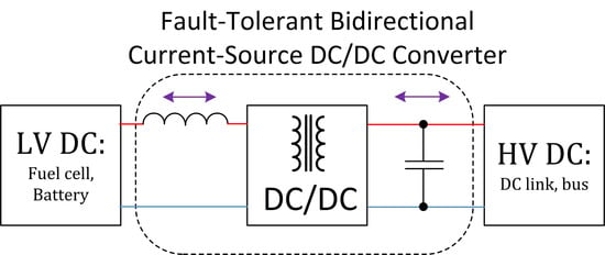
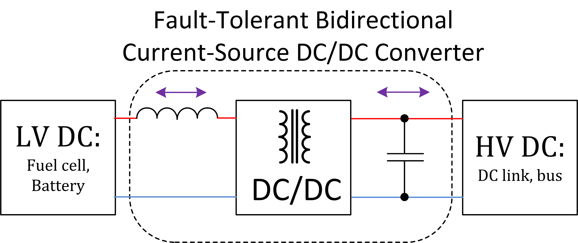
Present work is devoted to the assessment of the fault-tolerant capability of the bidirectional full-bridge current-source DC–DC converter on the basis of the topology presented in [11]. The number of semiconductor devices allows us to take advantage of different reconfiguration possibilities and address various post-failure operation modes. Current-source converters are inherently fault tolerant to internal and external short circuits [12,13], making it easier to handle this condition. Generally, after a failure, the topology can be reconfigured into another one with a simplified structure. The possibilities of such reconfigurations are addressed in Section 2, along with possible fault detection methods and procedures. The multi-mode operation strategy is addressed in Section 3. Finally, our assumptions are verified with experiments in Section 4.
2. Analysis of Case Study Current Source Converter
2.1. Description of Topology
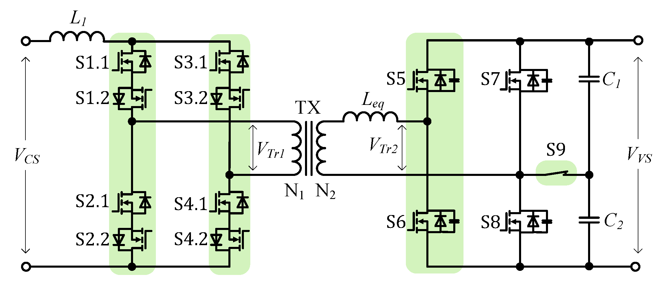
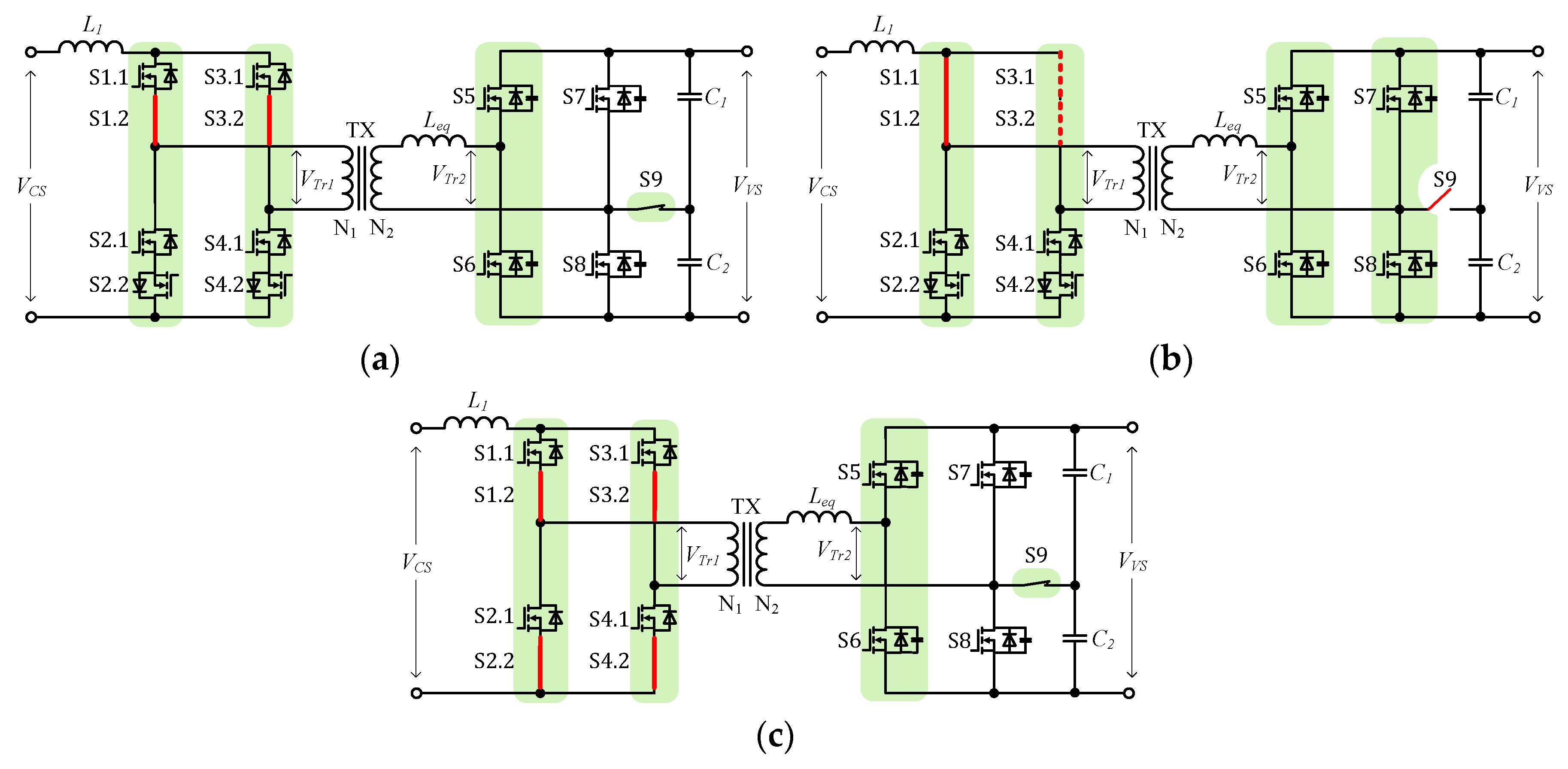
The isolated phase-shifted secondary modulated converter (PS-SMC) topology analyzed is presented in Figure 1 [10]. It features full-bridge at the current source (CS) side that utilizes bidirectional switches. At the secondary voltage source (VS) side, the hybrid structure is used. It can be reconfigured to either full- or half-bridge, using auxiliary switch S9 to compensate for the gain change in certain failure operating modes or to increase the converter regulation capabilities [10]. The bidirectional switch S9 can be realized by the semiconductor transistors or an electro-mechanical relay.
2.2. Analyzed Failure Modes
Despite significant improvements, semiconductor devices are still the power electronic converter components most susceptible to failure [1]. The reasons of failures and the failure type can vary, with strong dependence on the application area and operating conditions. In general, there are two types of failures of power semiconductor devices—open-circuit (OC) and short-circuit (SC). The OC condition can occur due to the gate drive failure, solder fatigue, or bond wire lift-off. On the other hand, SC failure can be the result of static or dynamic latch up, overvoltage, avalanche breakdown, etc. [12]. In some cases, the SC failure can lead to secondary effects that eventually result in an OC mode [14]. This work considers both OC and SC failure modes of one or several transistors in the topology and identifies possible reconfiguration possibilities.
A fault detection and diagnosis algorithm should be capable of locating the failed semiconductor and take action within a limited timeframe to avoid failure propagation to other components of the circuit. Thanks to inherent tolerance to SC conditions of the current-source topologies, the time available for the reconfiguration can be higher than that for voltage-source converters. On the other hand, the OC condition has to be addressed fast enough, as in this situation, the inductor creates overvoltage across the other healthy devices, which can fail due to the avalanche effect. Typical metal–oxide–semiconductor field-effect transistors (MOSFETs) are avalanche-rugged devices and can handle repetitive avalanche until their failure due to overheating, assuming the pulse energy is much lower than critical [14]. For the insulated-gate bipolar transistors (IGBTs), the avalanche ruggedness is smaller than the SC one due to high currents forming around the edge of the device and can vary significantly, depending on the device type and configuration [15,16,17].
2.3. Failure Detection Methods
Various OC and SC detection methods have been reported, which can be grouped into the following categories based on the operating principle:
- Desaturation detection;
- Shunt resistor;
- Current scaling (“mirror”);
- Gate charge (voltage);
- Inductive current rate of change (di/dt) sensing;
- Rogowski coil;
- Other/combined.
The desaturation method is a popular solution for IGBT [18]. This method is implemented in many driver integrated circuits and detects faults by monitoring collector-emitter voltage during the on-time of the transistor. After blanking time, this value is compared with a predetermined threshold to indicate SC or OC. This method can be effectively used for Si and SiC MOSFETs as well [19,20,21].
In the shunt resistor method, sort circuit protection is provided by monitoring the voltage across the metal film resistor connected in series with the transistor [22,23]. The voltage is then processed by a low-noise operational amplifier and compared to the reference value. A similar principle is applied in the current scaling method [24]. In this case, the current is monitored only through a part of the total die area, which allows for the reducing of the power losses in the shunt resistor. However, this method is mostly suitable at the integration into high-power transistor modules with several parallel transistor dies.
The gate charge method detects the difference in the gate-source voltage characteristics during the SC event [25]. It is associated with a lack of Miller plateau and the fast rise of gate-source voltage. The method is mostly applied to IGBTs, while its implementation with MOSFETs is associated with several challenges related to faster speed, ringing, smaller gate charge, and parameter variation between the devices [26].
The inductive sensing method is based on monitoring di/dt across stray inductance of the transistor module and can be used easily if gate-source and power source terminals are separated, providing a very fast response [27,28]. On the other hand, it cannot detect overcurrent at low di/dt, and its accuracy is highly influenced by the manufacturing tolerances.
The use of a Rogowski coil to detect fault conditions is addressed in [29]. The solution cannot detect the DC current and still remains quite complex for implementation due to parasitic oscillations and requirement of high-bandwidth amplifiers.
A combination of the methods can be used for better detection and protection characteristics. For example, the desaturation method together with di/dt sensing is analyzed in [30] to reduce blanking time. Likewise, the combination of gate voltage monitoring with di/dt achieves more robust SC and OC detection [31]. All of the mentioned methods or their combinations can be potentially applied for the detection of failure conditions in the case study current-source converter.
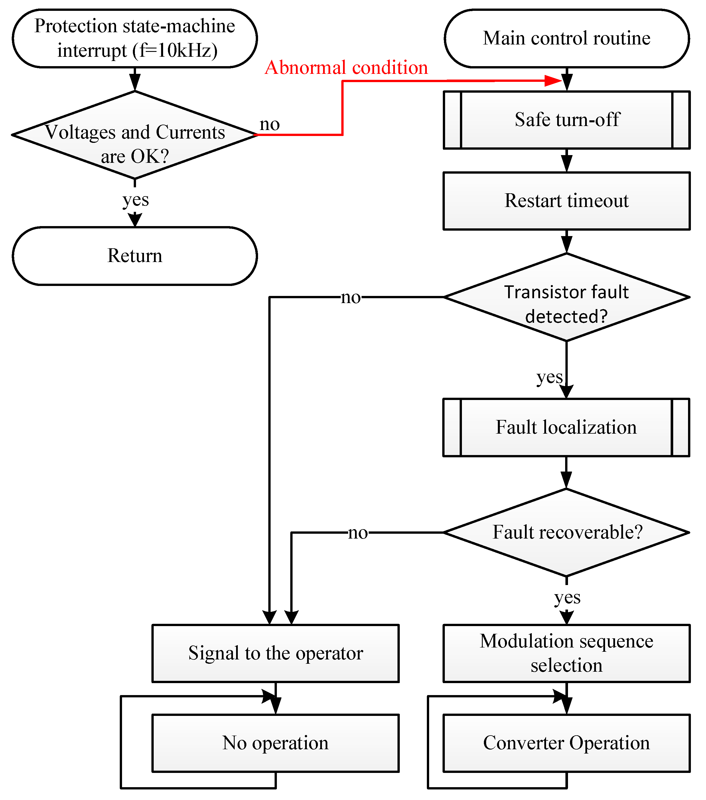
The reconfiguration approach assumes off-line detection of the faulty device during each start-up of the converter and selection of the appropriate control strategy to overcome the fault. The failure is detected according to the procedure in Figure 2.
2.4. Reconfiguration Possibilities and Post-Failure Modes
The converter in Figure 1 has high flexibility and offers several reconfiguration possibilities to other existing topologies from the group of snubberless current-source topologies:
Theoretically, reconfiguration to other topologies, like parallel-resonant converters [32,36,37,38], is also possible. However, that requires significant changes in the control and strongly affects the regulation capabilities. Moreover, the failure conditions that would require such reconfiguration are very specific and unlikely to happen. Therefore, these options are omitted from the current study.
The failure mode assumes malfunction of at least one of the transistors or the gate driver. After timely failure detection, localization, and definition, the appropriate topology reconfiguration should be made. As mentioned previously, the failed device is represented as an open- or short-circuit. In certain cases, several reconfiguration possibilities are possible; therefore, the most suitable option has to be identified based on the performance or functionality preserved.
The possible failure scenarios and reconfiguration possibilities are summarized in Table 1. The converter topology is assumed to be changed to one of those previously mentioned—A-SMC, FBK-SMC, or S-SMC in case a transistor fault is detected. It should be noticed that more than one failure can be tolerated for a particular reconfiguration option until the required fully operational devices are present. As it follows from Table 1, the CS side of the topology can tolerate a failure of any single transistor in either an open- or short-circuit state. Moreover, additional failure of certain gate drivers (“not active” condition) can be accepted as well.
Generally, the post-failure operation will impose certain restrictions on the converter operation due to increased power losses. At the SC failure of transistors S1.2 and/or S3.2, the converter should switch to the A-SMC mode, as shown in Figure 3a. In this mode, both S1.2 and S3.2 should be always turned on. Moreover, this mode can be used intentionally without any failures to increase the soft-switching range at low power levels; such a possibility will be discussed in the following section. Open- or short-circuit failure of any bidirectional switch can be overcome with reconfiguration to FBK-SMC. In this mode, either both top or bottom bidirectional switches operate at the switching frequency. One of the remaining bidirectional devices should be in the OC mode (or turned-off), while another in the SC mode (or turned-on) by the control system. The mode of the particular device is chosen according to its failure condition. An example of a converter with S1.1 and S1.2 in the SC condition and S3.1 and S3.2 in the OC condition is shown in Figure 3b. During the normal operation, the half-bridge is used at the VS side. In the case of reconfiguration to FBK-SMC, the voltage gain at the CS side is doubled. To compensate that, the switch S9 should be turned off and transistors S7 and S8 activated for the VS side to operate in the full-bridge mode. S-SMC mode, as shown in Figure 3c, should be used at the S2.2 and S4.2 SC failure. In this mode, the transistors S1.2, S2.2, S3.2, and S4.2 should be in the SC mode (or always turned on). Generally, this mode will have higher energy circulation and if possible, other reconfiguration options should be prioritized.
As observed from Table 1, the topology is sensitive to failures at the VS side. Neither open- nor short-circuit failures of bridge transistors can be tolerated. If the converter is intended to switch to the FBK-SMC mode, proper voltage rated devices have to be used at the CS side due to increased steady-state voltage stress in this mode. It should be noticed that the voltage rating of CS devices is dictated by the transient overvoltage peak present in the actively commutated inductive circuits [39] and depends on the converter parasitic parameters.
3. Multi-Mode Operation Strategy
As compared to most other current-source topologies without dedicated snubber circuits, the benefit of the studied PS-SMC converter lies in reduced energy circulation. The reason is that the converter current amplitude in the nominal operating mode never exceeds the CS-side current value and the transformer current is at zero during the shoot-through state. At the same time, this results in a limited capability of the converter to operate at low load conditions—the current in the circuit is not sufficient to recharge Ceq (representing equivalent parasitic capacitance of the circuit and external snubber capacitors, if applied). Moreover, this complicates the optimal selection of the duty cycle for VS-side transistors, as the time required for voltage polarity change can vary significantly, depending on the operating point. As a result, the zero-voltage switching (ZVS) capability of the converter is limited.
Although modulation with adaptive duty cycle can be implemented to reduce the body diode conduction time, it may not provide desired operation during fast changes in load or voltage. The A-SMC features the possibility to provide a soft-switching condition and wide range regulation even at no-load conditions. At the same time, its energy circulation is higher than in the PS-SMC. This section addresses the implementation possibility of multi-mode operation to enhance the regulation capability of the converter at light loads, while preserving the benefits of low energy circulation at high currents.
3.1. Converter Design Specifications
In the isolated boost-type topologies, the transformer primary voltage is always higher than the input one, which provides additional voltage step-up. At the same time, it is advantageous to limit the minimum voltage gain at the design stage for:
- Wider regulation capability;
- Reduced energy circulation;
- Increased transformer utilization;
- Reduced voltage stress on CS semiconductors.
All of these properties allow better utilization of converter components that will result in higher efficiency and increase of the overall practical feasibility. For the current case study, the application specification is defined according to the parameters listed in Table 2.
The operation of CS converters generally implies voltage overshoot associated with the diode reverse recovery process. In order to be able to safely use low voltage Si MOSFETs without snubbers at the CS side, its voltage has to be stabilized at the relatively low level. Therefore, the minimal normalized gain of <10% at the CS stage was chosen for the current study. To satisfy such criteria, the transformer with low leakage inductance is required, while the Ceq value should be selected carefully to obtain remarkable turn-off loss reduction of the VS devices with relatively low duty cycle loss.
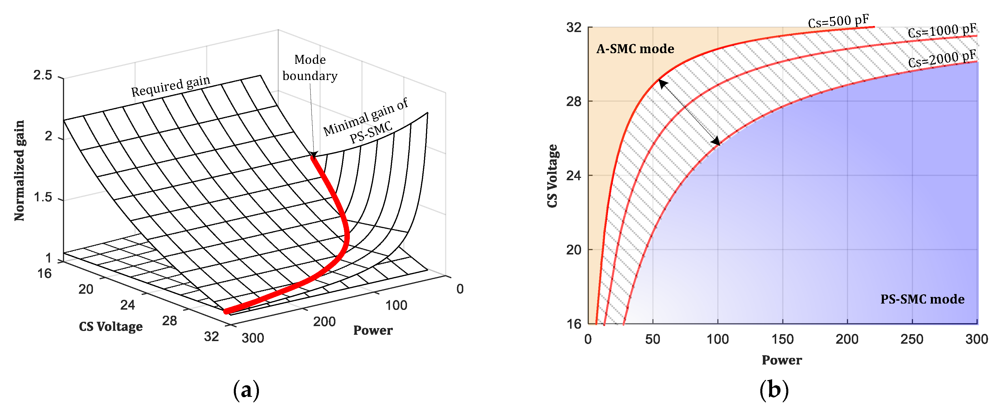
3.2. Determination of Mode Boundary
As was mentioned above, the resulting gain of the PS-SMC converter is determined by the active state loss due to equivalent inductance and capacitance present in the circuit. It is assumed that Leq is mainly represented by the transformer leakage inductance and Ceq is the equivalent capacitance referred to the CS side. In the calculations, the components are assumed lossless, the transformer magnetizing inductance is assumed to be infinitely large, and the CS-side current ripple is neglected. The equivalent capacitance is estimated as
The converter normalized gain in a general form is defined as
The converter gain at the CS side is calculated as follows [10]:
where ICS is the CS side current and is the maximum CS side current (estimated for minimum input voltage and full load).
On the other hand, the A-SMC converter [17] features improved regulation capability, since Ceq is always discharged with maximal current . The converter gain is calculated as
where tres is the duration of the resonant interval [17].
Using Equations (3) and (4), the minimal values were derived for PS-SMC and A-SMC. The intersection of these values with the normalized gain according to Equation (2) provides the borderline between the PS-SMC and A-SMC modes, as shown in Figure 4. In the latter mode, the transistors S1.2 and S3.2 are turned on to allow more current to accumulate in the circuit for the discharge of Ceq, enabling an extended output voltage regulation range. It should be noticed that the borderlines show theoretical values that can be achieved with ideal converter parameter values for particular operating points. In the practical systems, a trade-off is necessary in order to simplify control and optimize the performance, along with a certain design safety margin. This will affect the borderline and will be discussed in more detail in the following section.
4. Results
4.1. Post-Failure Operation and Performance
To validate the analysis from the previous section, a converter prototype according to the topology from Figure 1 and specifications listed in Table 2 was tested. The OC or SC conditions for semiconductors were emulated by the microcontroller by keeping the corresponding gating signal of the transistor “off” and “on”, respectively. The system operated in the open-loop and fault diagnostics was not applied. The focus was on the converter performance and capabilities when operating under various post-failure conditions.
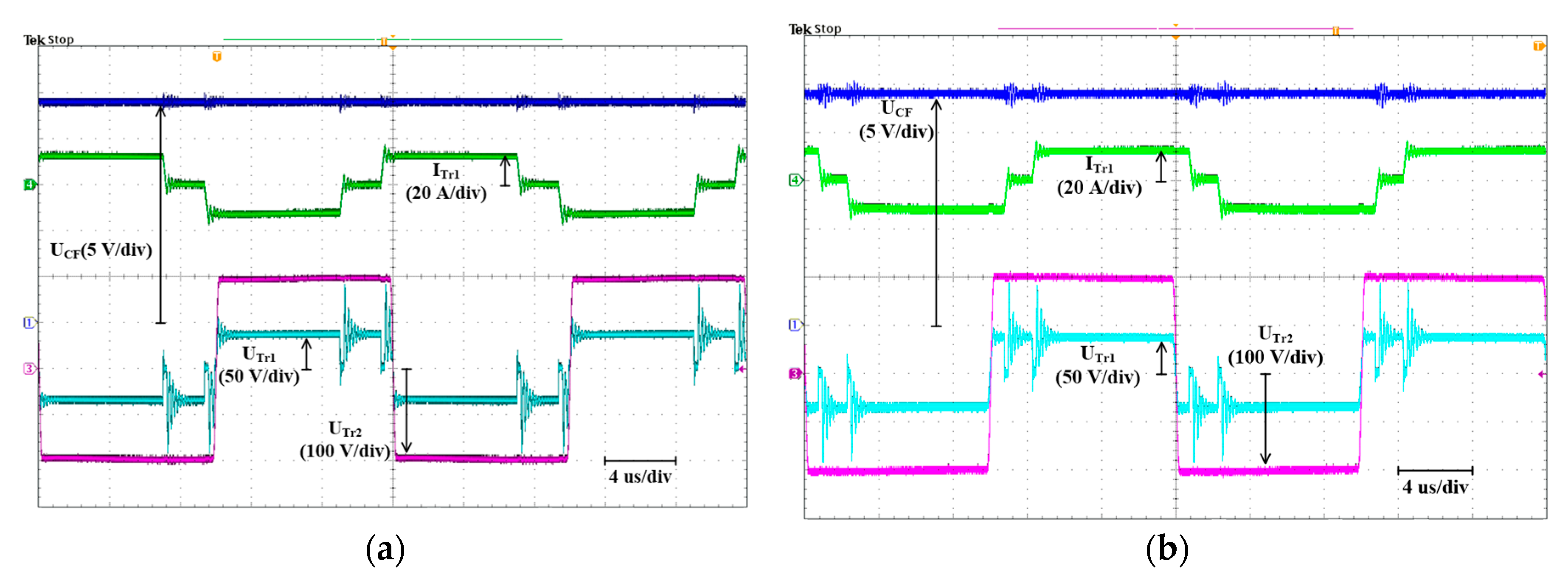
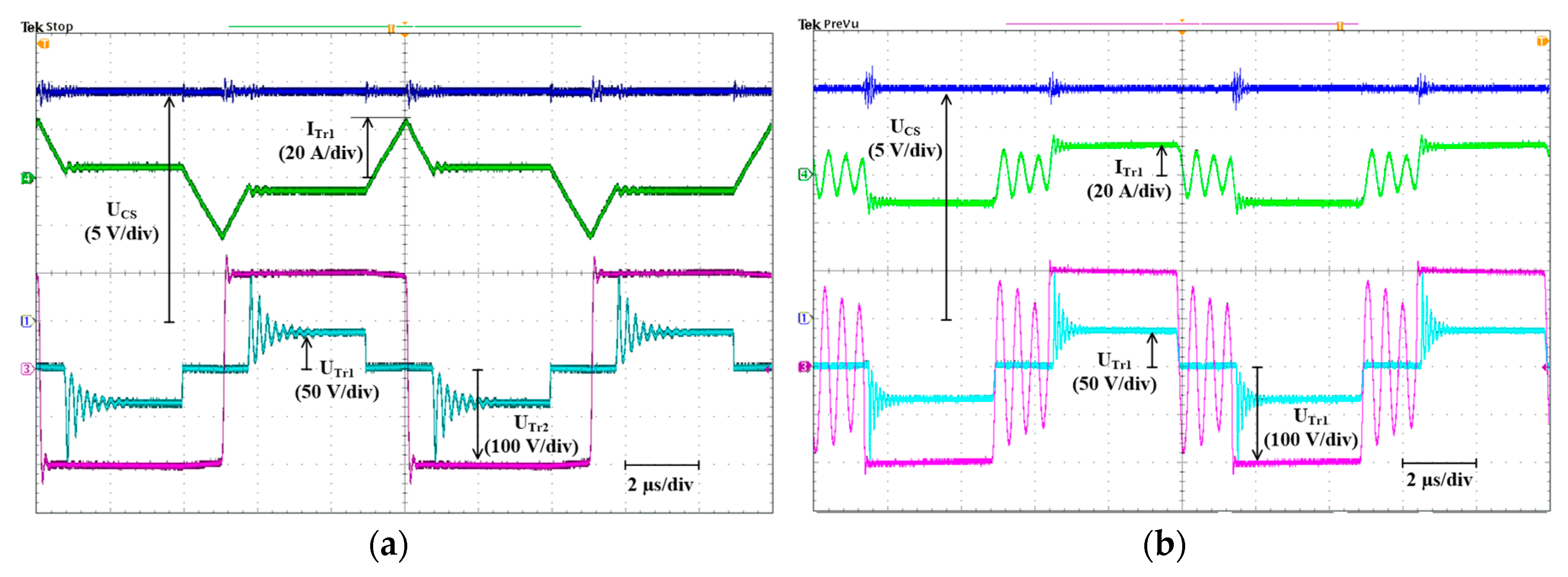
The normal operation of PS-SMC in boost and buck modes is presented in Figure 5a,b, respectively. At the post-failure reconfiguration to the A-SMC topology, as shown in Table 1, the transistors S1 and S3 and the transformer are operating with increased peak current, as shown in Figure 6 are preserved. As was mentioned, this topology allows even a wider regulation range than the reference PS-SMC; the experimental results and analysis addressing this feature are presented in the following section.
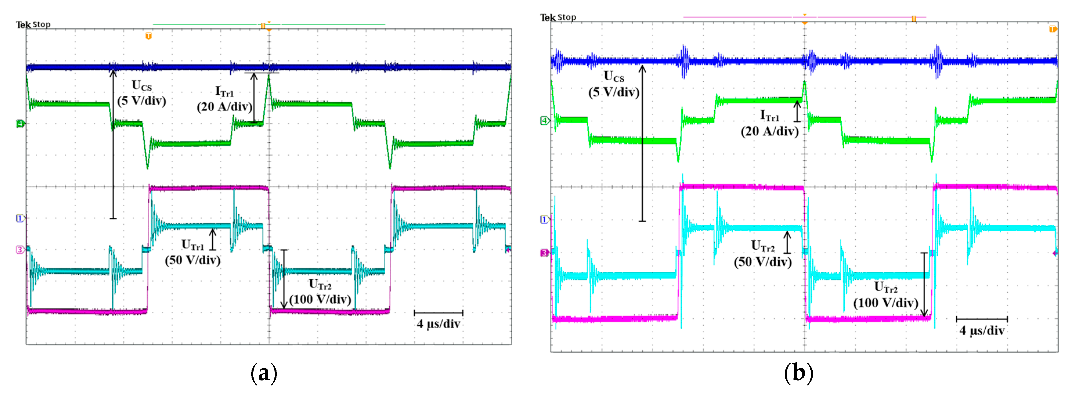
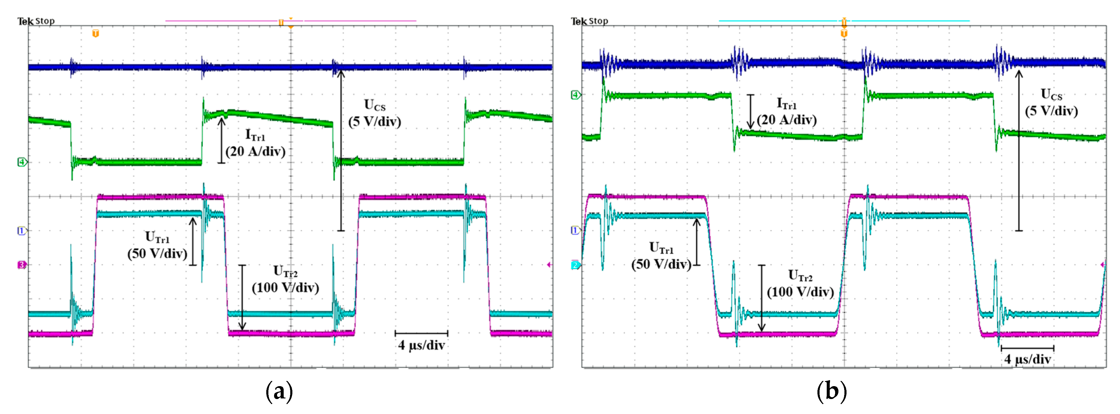
The operating waveforms after the reconfiguration of the S-SMC topology are shown in Figure 7. Similar to the previously described failure mode (A-SMC), the peak current in the circuit is increased, while the gain on the reference topology is preserved. As was observed, there is no zero-current interval at the transformer, and thus the amount of circulating current is generally higher than in other configurations. Therefore, other post-failure reconfigurations should be prioritized whenever possible.
As it follows from T, the reconfiguration to FBK-SMC can be used in the case of many various failure modes, particularly if there is an OC switch condition at the CS side. As compared to the reference case, the gain of the topology is double, and the VS-side is reconfigured to the full-bridge to compensate that. The experimental waveforms are presented in Figure 8.
4.2. Multi-Mode Control
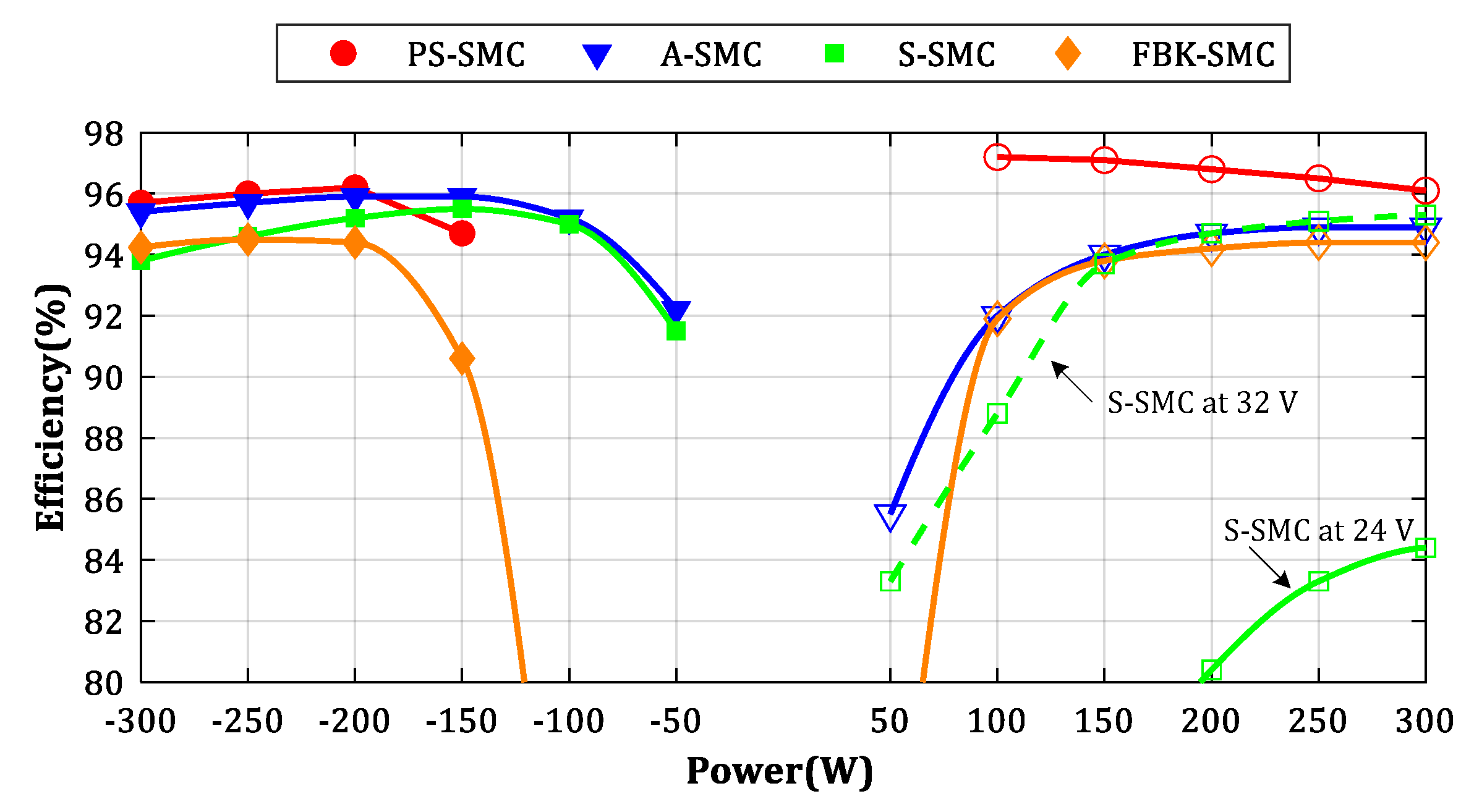
To estimate the performance in the post-failure modes, the total efficiency of different configurations above was measured using a Yokogawa WT3000 power analyzer at the room temperature of 25 °C, as shown in Figure 9. It follows that the converter can tolerate most fault conditions without significant reduction of the efficiency. In certain cases, when the S-SMC mode is used at low CS-side voltages, certain power derating may be necessary to keep the operating temperature within required limits. Alternatively, in the FBK-SMC mode, the reduction in the efficiency at light loads is expected due to the loss of ZVS.
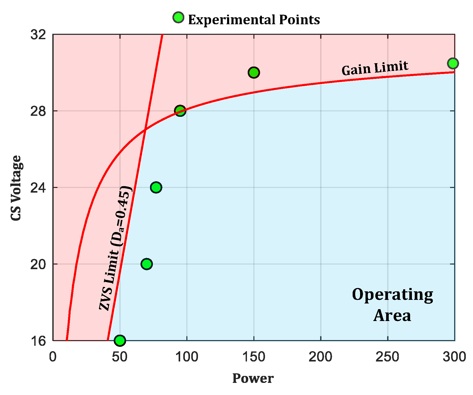
In order to implement the multi-mode control strategy, the operating limits of the PS-SMC converter prototype have to be determined taking into account the parameters defined. It was assumed that the converter is controlled with phase-shift control, while the other operating parameters are set to be constant, as listed in Table 2. The estimated and experimentally obtained operating limits of the prototype are depicted in Figure 10. The experimentally obtained values are close to the theoretical ones, while the observed deviation can be explained by a slight mismatch in the component values and power losses in the circuit. It follows that the regulation capability of the converter may be limited due to two different factors—at high CS voltage, the converter cannot deliver the required output voltage due to limited minimal gain (active state loss), while at low loads, it loses the ZVS of VS-side devices due to the increased recharge time of capacitors. For the current study, the parameters were chosen to demonstrate the flexibility of the converter design in general, while the optimal values can be selected according to a particular application and its operating profile.
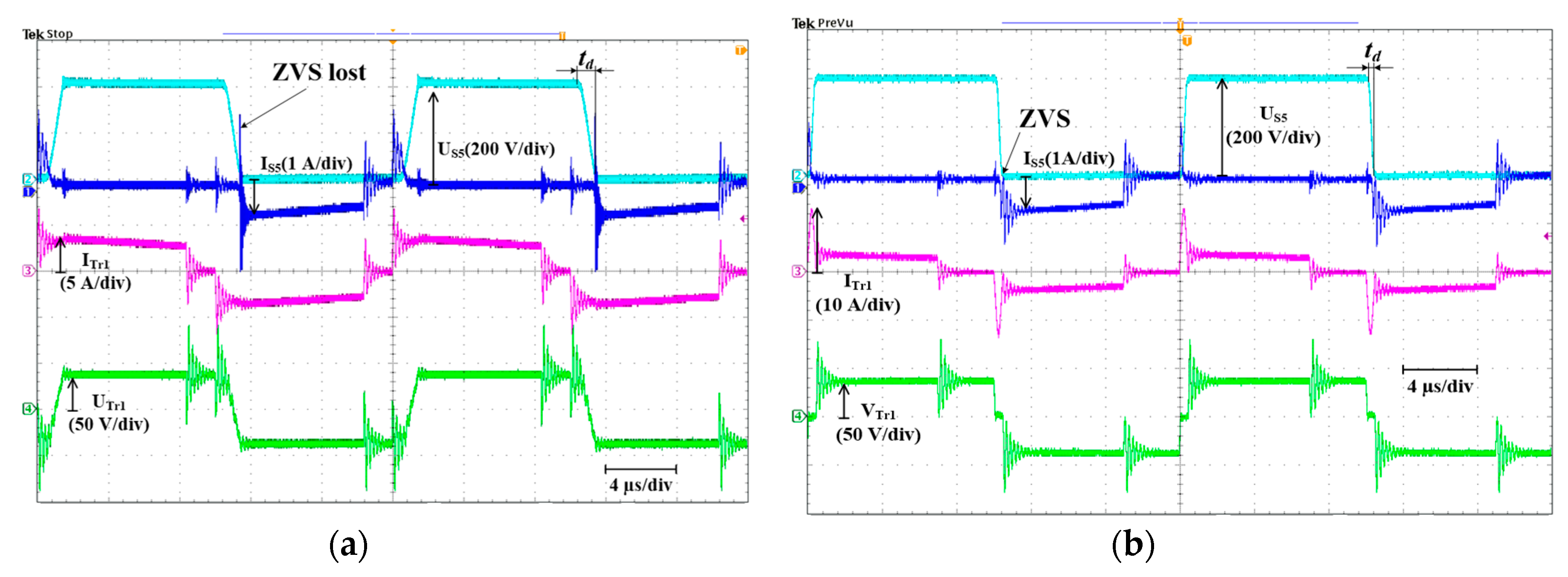
The waveforms demonstrating the loss of ZVS at 80 W are presented in Figure 11a. The multi-mode operation allows the topology to change to A-SMC and overcome the regulation limitations. An example is illustrated in Figure 11b, where it is shown that the capacitor discharge time (td) was significantly reduced in the A-SMC topology due to increased peak current. On the other hand, this results in the increased energy circulation in the topology, therefore baseline PS-SMC mode should be prioritized if the current in the circuit is sufficient for ZVS.
5. Conclusions
This work addresses fault-tolerant operating capabilities of the bidirectional full-bridge current-source converter with secondary-modulation. According to the presented analysis, the converter can tolerate both open- and short-circuit conditions at the low-voltage CS side, assuming a hybrid full/half-bridge circuit used at the high-voltage side. This is achieved by the reconfiguration of the baseline PS-SMC into other known topology types (S-SMC, A-SMC, S-SMC), depending on the failed device location and failure mode. The expected reduction of the efficiency in the post-fault cases is within 2% at maximum power. Although higher reduction in efficiency is expected at lower power levels due to increased energy circulation or loss of ZVS, the bidirectional capability is preserved, and the general functionality provided. At the same time, it was revealed that failures at the high voltage VS-side cannot be tolerated using the reconfiguration principles of the analyzed topology.
Moreover, it was predicted and experimentally confirmed that the A-SMC mode can be applied as a multi-mode strategy to extend the ZVS range of the baseline converter. This allows the converter to easily handle no-load conditions even with relatively large external snubber capacitors.
Author Contributions
Conceptualization, A.B. and R.K.; methodology, A.B. and R.K.; validation, R.K. and A.C.; formal analysis, A.B. and V.I.; investigation, A.B., R.K., and V.I.; software, R.K.; writing—original draft preparation, A.B. and R.K.; visualization, A.B., R.K., and A.C.; supervision, V.I. and A.C.; project administration, A.C.
Funding
This research was supported by the Estonian Centre of Excellence in Zero Energy and Resource Efficient Smart Buildings and Districts, ZEBE, grant 2014-2020.4.01.15-0016 funded by the European Regional Development Fund and by the Estonian Research Council grant PSG206.
Conflicts of Interest
Authors declare no conflict of interest.
References
- Falck, J.; Felgemacher, C.; Rojko, A.; Liserre, M.; Zacharias, P. Reliability of Power Electronic Systems: An Industry Perspective. IEEE Ind. Electron. Mag. 2018, 12, 24–35. [Google Scholar] [CrossRef]
- Ghimire, P.; Beczkowski, S.; Munk-Nielsen, S.; Rannestad, B.; Thogersen, P.B. A review on real time physical measurement techniques and their attempt to predict wear-out status of IGBT. In Proceedings of the 15th European Conference Power Electronics and Applications (EPE), Lille, France, 2–6 September 2013; pp. 1–10. [Google Scholar]
- Falck, J.; Andresen, M.; Liserre, M. Active methods to improve reliability in power electronics. In Proceedings of the 43rd Annual Conference IEEE Industrial Electronics Society, Beijing, China, 29 October–1 November 2017; pp. 7923–7928. [Google Scholar]
- Oh, H.; Han, B.; McCluskey, P.; Han, C.; Youn, B.D. Physics-of-Failure, Condition Monitoring, and Prognostics of Insulated Gate Bipolar Transistor Modules: A Review. IEEE Trans. Power Electron. 2015, 30, 2413–2426. [Google Scholar] [CrossRef]
- Wang, H.; Blaabjerg, F. Reliability of Capacitors for DC-Link Applications in Power Electronic Converters—An Overview. IEEE Trans. Ind. Appl. 2014, 50, 3569–3578. [Google Scholar] [CrossRef]
- Best Practices in Photovoltaic System Operations and Maintenance; Technical Report, NREL/TP-7A40-67553; National Renewable Energy Laboratory (NREL): Lakewood, CO, USA, 2016.
- Zhang, W.; Xu, D.; Enjeti, P.N.; Li, H.; Hawke, J.T.; Krishnamoorthy, H.S. Survey on Fault-Tolerant Techniques for Power Electronic Converters. IEEE Trans. Power Electron. 2014, 29, 6319–6331. [Google Scholar] [CrossRef]
- Jovanović, M.M.; Irving, B.T. On-the-Fly Topology-Morphing Control—Efficiency Optimization Method for LLC Resonant Converters Operating in Wide Input- and/or Output-Voltage Range. IEEE Trans. Power Electron. 2016, 31, 2596–2608. [Google Scholar] [CrossRef]
- Kumar, A.; Lu, J.; Afridi, K.K. Power Density and Efficiency Enhancement in ICN DC–DC Converters Using Topology Morphing Control. IEEE Trans. Power Electron. 2019, 34, 1881–1900. [Google Scholar] [CrossRef]
- Costa, L.; Buticchi, G.; Liserre, M. A Fault-Tolerant Series-Resonant DC–DC Converter. IEEE Trans. Power Electron. 2017, 32, 900–905. [Google Scholar] [CrossRef]
- Blinov, A.; Kosenko, R.; Chub, A.; Vinnikov, D. Bidirectional soft-switching dc–dc converter for battery energy storage systems. IET Power Electron. 2018, 11, 2000–2009. [Google Scholar] [CrossRef]
- Lutz, J.; Schlangenotto, H.; Scheuermann, U.; Doncker, R.D. Semiconductor Power Devices: Physics Characteristics Reliability; Springer: New York, NY, USA, 2011. [Google Scholar]
- Kosenko, R.; Chub, A.; Blinov, A. Full-soft-switching high step-up bidirectional isolated current-fed push-pull DC-DC converter for battery energy storage applications. In Proceedings of the 42nd Annual Conference IEEE Industrial Electronics Society, Florence, Italy, 24–27 October 2016; pp. 6548–6553. [Google Scholar]
- Dchar, I.; Buttay, C.; Morel, H. Avalanche Robustness of SiC Schottky Diode. Microelectronics Reliability. 2016. Available online: https://hal.archives-ouvertes.fr/hal-01373039 (accessed on 20 August 2019).
- Blinov, A.; Norrga, S.; Tibola, G. Operation of single-chip MOSFET and IGBT devices after failure due to repetitive avalanche. In Proceedings of the 17th European Conference on Power Electronics and Applications (EPE’15 ECCE-Europe), Geneva, Switzerland, 8–10 September 2015; pp. 1–9. [Google Scholar]
- Lu, J.; Tian, X.; Jin, L.; Lu, S.; Zhou, H.; Zhu, Y.; Han, Z. Dynamic avalanche behavior of power MOSFETs and IGBTs under unclamped inductive switching conditions. J. Semiconductors 2013, 34, 26–30. [Google Scholar] [CrossRef]
- IGBT Ruggedness. ON Semiconductor; Application Note AND9127/D; Semiconductor Components Industries, LLC: Aurora, CO, USA, 2016; Available online: https://www.onsemi.com/pub/Collateral/AND9127-D.pdf (accessed on 20 August 2019).
- Lu, B.; Sharma, S. A Literature Review of IGBT Fault Diagnostic and Protection Methods for Power Inverters. In Proceedings of the IEEE Industry Applications Society Annual Meeting, Edmonton, AB, Canada, 5–9 October 2008; pp. 1–8. [Google Scholar]
- Bertelshofer, T.; Maerz, A.; Bakran, M. Design Rules to Adapt the Desaturation Detection for SiC MOSFET Modules. In Proceedings of the International Exhibition and Conference for Power Electronics, Intelligent Motion, Renewable Energy and Energy Management (PCIM Europe 2017), Nuremberg, Germany, 16–18 May 2017; pp. 1–8. [Google Scholar]
- Sadik, D.; Colmenares, J.; Tolstoy, G.; Peftitsis, D.; Bakowski, M.; Rabkowski, J.; Nee, H.-P. Short-Circuit Protection Circuits for Silicon-Carbide Power Transistors. IEEE Trans. Ind. Electron. 2016, 63, 1995–2004. [Google Scholar] [CrossRef]
- Wang, Z.; Shi, X.; Xue, Y.; Tolbert, L.M.; Blalock, B.J.; Wang, F. Design and performance evaluation of overcurrent protection schemes for silicon carbide (SiC) power MOSFETs. In Proceedings of the IEEE Energy Conversion Congress and Exposition, Denver, CO, USA, 15–19 September 2013; pp. 5418–5425. [Google Scholar]
- Spang, M.; Hofstoetter, N. Evaluation of Current Measurement Accuracy for a Power Module with Integrated Shunt Resistors. In Proceedings of the PCIM Europe 2017 International Exhibition and Conference for Power Electronics, Intelligent Motion, Renewable Energy and Energy Management, Nuremberg, Germany, 10–12 May 2017; pp. 1–8. [Google Scholar]
- Jeong, J.; Lee, J.; Lee, S.; Tsukizawa, M. Effective resistor selection method for over current protection when using sense IGBT solution. In Proceedings of the International ECTI Northern Section Conference on Electrical, Electronics, Computer and Telecommunications Engineering (ECTI-NCON), Chiang Rai, Thailand, 25–28 February 2018; pp. 40–43. [Google Scholar]
- Fink, K.; Volke, A.; Wei, W.; Wiesner, E.; Thal, E. Gate-Driver with Full Protection for SiC-MOSFET Modules. In Proceedings of the International Exhibition and Conference for Power Electronics, Intelligent Motion, Renewable Energy and Energy Management (PCIM Asia 2016), Shanghai, China, 28–30 June 2016; pp. 1–7. [Google Scholar]
- Horiguchi, T.; Kinouchi, S.; Nakayama, Y.; Oi, T.; Urushibata, H.; Okamo, S.; Tominaga, S.; Akagi, H. A high-speed protection circuit for IGBTs subjected to hard-switching faults. In Proceedings of the IEEE Applied Power Electronics Conference and Exposition—APEC 2014, Fort Worth, TX, USA, 16–20 March 2014; pp. 2519–2525. [Google Scholar]
- Climaco-Arvizu, O.; Hernández-González, L.; Rodríguez-Blanco, M.A. Fault detection for SiC-Mosfet based on the behavior of gate signal. In Proceedings of the IEEE 10th International Symposium on Diagnostics for Electrical Machines, Power Electronics and Drives (SDEMPED), Guarda, Portugal, 1–4 September 2015; pp. 71–76. [Google Scholar]
- Huang, F.; Flett, F. IGBT Fault Protection Based on di/dt Feedback Control. In Proceedings of the IEEE Power Electronics Specialists Conference, Orlando, FL, USA, 17–21 June 2007; pp. 1478–1484. [Google Scholar]
- Oinonen, M.; Laitinen, M.; Kyyrä, J. Current measurement and short-circuit protection of an IGBT based on module parasitics. In Proceedings of the 16th European Conference on Power Electronics and Applications, Lappeenranta, Finland, 26–28 August 2014; pp. 1–9. [Google Scholar]
- Wang, J.; Shen, Z.; Burgos, R.; Boroyevich, D. Design of a high-bandwidth Rogowski current sensor for gate-drive shortcircuit protection of 1.7 kV SiC MOSFET power modules. In Proceedings of the IEEE 3rd Workshop on Wide Bandgap Power Devices and Applications (WiPDA), Blacksburg, VA, USA, 2–4 November 2015; pp. 104–107. [Google Scholar]
- Velander, E.; Kruse, L.; Meier, S.; Löfgren, A.; Wiik, T.; Nee, H.-P.; Sadik, D.-P. Analysis of short circuit type II and III of high voltage SiC MOSFETs with fast current source gate drive principle. In Proceedings of the IEEE 8th International Power Electronics and Motion Control Conference (IPEMC-ECCE Asia), Hefei, China, 22–26 May 2016; pp. 3392–3397. [Google Scholar]
- Hain, S.; Bakran, M. New Ultra Fast Short Circuit Detection Method Without Using the Desaturation Process of the Power Semiconductor. In Proceedings of the International Exhibition and Conference for Power Electronics, Intelligent Motion, Renewable Energy and Energy Management (PCIM Europe 2016), Nuremberg, Germany, 10–12 May 2016; pp. 1–8. [Google Scholar]
- Kosenko, R.; Blinov, A.; Chub, A.; Vinnikov, D. Asymmetric Snubberless Current-Fed Full-Bridge Isolated DC-DC Converters. Electr. Control Commun. Eng. 2018, 14, 5–11. [Google Scholar] [CrossRef]
- Blinov, A.; Kosenko, R.; Chub, A.; Vinnikov, D. Bidirectional Soft Switching Current Source DC-DC Converter for Residential DC Microgrids. In Proceedings of the IECON 2018—44th Annual Conference of the IEEE Industrial Electronics Society, Washington, DC, USA, 21–23 October 2018; pp. 6059–6064. [Google Scholar]
- Kosenko, R.; Vinnikov, D. Soft-Switching Current-FED Flyback Converter with Natural Clamping for Low Voltage Battery Energy Storage Applications. In Technological Innovation for Smart Systems, Proceedings of the Doctoral Conference on Computing, Electrical and Industrial Systems, Lisbon, Portugal, 3–5 May 2017; Springer International Publishing: Basel, Switzerland, 2017. [Google Scholar]
- Xuewei, P.; Rathore, A.K. Novel Interleaved Bidirectional Snubberless Soft-Switching Current-Fed Full-Bridge Voltage Doubler for Fuel-Cell Vehicles. IEEE Trans. Power Electron. 2013, 28, 5535–5546. [Google Scholar] [CrossRef]
- Chen, R.Y.; Liang, T.J.; Chen, J.F.; Lin, R.L.; Tseng, K.C. Study and Implementation of a Current-Fed Full-Bridge Boost DC-DC Converter with Zero-Current Switching for High-Voltage Applications. IEEE Trans. Ind. Appl. 2008, 44, 1218–1226. [Google Scholar] [CrossRef]
- Iannello, C.; Luo, S.; Batarseh, I. Full bridge ZCS PWM converter for high-voltage high-power applications. IEEE Trans. Aerosp. Electron. Syst. 2002, 38, 515–526. [Google Scholar] [CrossRef]
- Blinov, A.; Kosenko, R.; Chub, A.; Vinnikov, D. Snubberless boost full-bridge converters: Analysis of soft switching performance and limitations. Int. J. Circuit Theor. Appl. 2019, 47, 884–908. [Google Scholar] [CrossRef]
- Mößlacher, C.; Guillemant, O. Improving Efficiency of Synchronous Rectification by Analysis of the MOSFET Power Loss Mechanism; Application Note AN 2012-03; Infineon Technologies Austria AG: Villach, Austria, 2012; Available online: https://www.infineon.com/dgdl/Infineon-MOSFET_OptiMOS_improving_efficiency_of_synchronous_rectification_by_analysis_of_the_MOSFET_power_loss_mechanism-AN-v03_00-EN.pdf?fileId=db3a304320d39d590121a671f2d90c38 (accessed on 20 August 2019).
Figure 1.
Analyzed PS-SMC converter topology with a reconfigurable rectifier.

Figure 2.
Generalized fault detection procedure for the case study current source converter.

Figure 3.
Reconfiguration possibilities of the case study converter: asymmetric secondary-modulated converter (A-SMC): (a), flyback secondary-modulated converter (FBK-SMC) (b), and symmetric secondary-modulated converter (S-SMC) (c).
Figure 3.
Reconfiguration possibilities of the case study converter: asymmetric secondary-modulated converter (A-SMC): (a), flyback secondary-modulated converter (FBK-SMC) (b), and symmetric secondary-modulated converter (S-SMC) (c).

Figure 4.
Derivation of the borderline between PS- and A-SMC modes for Cs = 1 nF (a); theoretical mode boundaries for various Cs values (b).
Figure 4.
Derivation of the borderline between PS- and A-SMC modes for Cs = 1 nF (a); theoretical mode boundaries for various Cs values (b).

Figure 5.
Operating waveforms in the PS-SMC mode: boost (a) and buck (b). UCS = 24 V, P = 300 W.

Figure 6.
Operating waveforms in the A-SMC mode: boost (a) and buck (b). UCS = 24 V, P = 300 W.

Figure 7.
Operating waveforms in the S-SMC mode: boost (a) and buck (b). UCS = 24 V, P = 300 W.

Figure 8.
Operating waveforms in the FBK-SMC mode: boost (a) and buck (b). UCS = 24 V, P = 300 W.

Figure 9.
Measured efficiencies in different operating modes at UCS = 24 V (unless otherwise specified); negative power values denote buck mode, positive-boost mode.
Figure 9.
Measured efficiencies in different operating modes at UCS = 24 V (unless otherwise specified); negative power values denote buck mode, positive-boost mode.

Figure 10.
Theoretical and experimental operating boundaries.

Figure 11.
Operation in the PS-SMC mode demonstrating the loss of zero-voltage switching (ZVS) (a); operation in the A-SMC mode with reduced recharge time td (b). UCS = 24 V, PCS = 80 V.
Figure 11.
Operation in the PS-SMC mode demonstrating the loss of zero-voltage switching (ZVS) (a); operation in the A-SMC mode with reduced recharge time td (b). UCS = 24 V, PCS = 80 V.


Table 1.
Acceptable failures and reconfiguration possibilities A.
| Transistor | PS-SMC | A-SMC | FBK-SMC | S-SMC | |||
|---|---|---|---|---|---|---|---|
| S1.1 | + | + | 1 | + | 0/- | + | + |
| S1.2 | + | 1 | 1 | + | 0/- | + | 1 |
| S2.1 | + | + | + | 1 | + | 0/- | + |
| S2.2 | + | + | + | 1 | + | 0/- | 1 |
| S3.1 | + | + | 0/- | + | 1 | + | + |
| S3.2 | + | 1 | 0/- | + | 1 | + | 1 |
| S4.1 | + | + | + | 0/- | + | 1 | + |
| S4.2 | + | + | + | 0/- | + | 1 | 1 |
| S5 | + | + | + | + | + | + | + |
| S6 | + | + | + | + | + | + | + |
| S7 | - | - | + | + | + | + | - |
| S8 | - | - | + | + | + | + | - |
| S9 | - | - | +/1 | +/1 | +/1 | +/1 | - |
A “+”—fully operational, “1”—short-circuit (SC) failure or turned on, “0”—OC failure, “-”—not active or gate drive failure.
Table 2.
Main converter parameters and components. CS: current source; VS: voltage source.
| Parameter/Component | Symbol | Value |
|---|---|---|
| CS voltage | UCS | 16–32 VDC |
| VS voltage | UVS | 380–420 VDC |
| Power | Prated | 300 W |
| Operating frequency | fsw | 50 kHz |
| Transformer turns ratio | n | 5.5 |
| CS side Inductor | L1 | 100 μH |
| Equivalent switch capacitance | Cs | 500 pF |
| Equivalent inductance | Leq | 400 nH |
| CS MOSFETs | S1.x–S4.x | BSC035N10NS5 |
| VS MOSFETs | S5–S6 | IXFP22N65X2 |
© 2019 by the authors. Licensee MDPI, Basel, Switzerland. This article is an open access article distributed under the terms and conditions of the Creative Commons Attribution (CC BY) license (http://creativecommons.org/licenses/by/4.0/).
Share and Cite
MDPI and ACS Style
Blinov, A.; Kosenko, R.; Chub, A.; Ivakhno, V. Analysis of Fault-Tolerant Operation Capabilities of an Isolated Bidirectional Current-Source DC–DC Converter. Energies 2019, 12, 3203. https://doi.org/10.3390/en12163203
AMA Style
Blinov A, Kosenko R, Chub A, Ivakhno V. Analysis of Fault-Tolerant Operation Capabilities of an Isolated Bidirectional Current-Source DC–DC Converter. Energies. 2019; 12(16):3203. https://doi.org/10.3390/en12163203
Chicago/Turabian StyleBlinov, Andrei, Roman Kosenko, Andrii Chub, and Volodymyr Ivakhno. 2019. "Analysis of Fault-Tolerant Operation Capabilities of an Isolated Bidirectional Current-Source DC–DC Converter" Energies 12, no. 16: 3203. https://doi.org/10.3390/en12163203
Note that from the first issue of 2016, this journal uses article numbers instead of page numbers. See further details here.