Evaluation of Electric Field and Space Charge Dynamics in Dielectric under DC Voltage with Superimposed Switching Impulse


Department of Electrical and Electronic Engineering, Hanyang University, Ansan 15588, Korea
*
Author to whom correspondence should be addressed.
Energies 2019, 12(10), 1836; https://doi.org/10.3390/en12101836
Submission received: 19 April 2019
/
Revised: 7 May 2019
/
Accepted: 12 May 2019
/
Published: 15 May 2019
(This article belongs to the Section F: Electrical Engineering)
Abstract
:The influx of a switching impulse during DC steady-state operations causes severe electrical stress on the insulation of HVDC cables. Thus, the insulation should be designed to withstand a superimposed switching impulse. All major manufacturers of DC cables perform superimposed switching impulse breakdown tests for prequalification. However, an experimental approach to study space charge dynamics in dielectrics under a switching impulse superposed on DC voltage has not been reported yet. This is because, unlike the DC stress, it is not possible to study the charge dynamics experimentally under complex stresses, such as switching impulse superposition. Hence, in order to predict and investigate the breakdown characteristics, it is necessary to obtain accurate electric field distribution considering space charge dynamics using a numerical approach. Therefore, in this paper, a numerical study on the switching impulse superposition was carried out. The space charge dynamics and its distribution within the dielectric under DC stress were compared with those under a superimposed switching impulse using a bipolar charge transport (BCT) model. In addition, we estimated the effect of a superimposed switching impulse on a DC electric field distribution. It was concluded that the temperature conditions of dielectrics have a significant influence on electric field and space charge dynamics.
1. Introduction
A switching impulse superimposed on a DC voltage causes severe overvoltage stress that can cause dielectric breakdown in an HVDC cable system. It causes a significant potential difference, instantaneously resulting in increased electrical stress for a period of several microseconds [1]. Therefore, consideration of this superposition situation is vital for the design of insulation in HVDC cables. In recognition of the danger of breakdown, an electrical breakdown test considering superimposed switching impulse voltage has been strongly recommended for HVDC cables in recent literature [2,3].
However, it is quite difficult to experimentally study the microscopic phenomenon that results from switching impulse superposition [4]. Therefore, a numerical approach needs to be devised for studying the space charge dynamics and electric field distribution under superimposed switching impulse. This kind of information is paramount for optimal and compact insulation design.
In this paper, low-density polyethylene (LDPE) was selected as the dielectric for numerical study. The application of high DC voltage causes the generation and transport of charge inside the polyethylene-based insulation materials. This results in an inevitable accumulation of space charge inside the insulation material [5,6]. This space charge accumulation not only distorts the electric field distribution under DC stress, but also causes the deterioration of insulating materials in the long term. Consequently, by understanding the impact of space charge on insulating materials, we can answer the problematic issues such as increase of the working stresses, lifetime prediction, and development of improved materials [7].
A bipolar charge transport (BCT) model was applied to numerically evaluate the space charge behavior and electric field distribution under DC voltage and superimposed switching impulse. In this simulation, the switching impulse was applied to the system under prestress DC voltage after reaching DC steady state. When considering the complex stresses resulting from two different sources, a suitable coupling should be adopted. Coupling of the switching impulse with the prestress DC voltage is quite intricate considering the various continuities to be considered for the two systems. For avoiding an unstable integration, the continuity of all equations at the moment when the switching impulse was superimposed is maintained.
In this work, charge transport properties of LDPE under the application of DC voltage were numerically analyzed in terms of rates of generation and loss of charge carriers. We have also discussed the space charge dynamics under switching impulse superimposed on the prestress DC voltage. In addition, we have obtained the electric field distribution according to temperature and applied voltage types (i.e., DC voltage or DC voltage with superimposed switching impulse). The maximum electric field intensity caused by DC voltage with superimposed switching impulse was compared with that of pure DC to assess the effect of the switching impulse.
2. Mechanism of Bipolar Charge Transport Model
The BCT model is designed to estimate space charge dynamics in polyethylene-based dielectrics used in HVDC cables [4,5,6,7,8,9,10]. It can overcome the following limitations of an electrical conductivity-based model.
- Under practical conditions, dielectric material is not homogenous, and local conditions can affect the transport processes and result in localized accumulations of space charge [8].
- It cannot account for the complicated charge transport mechanisms, including charge injection at the electrode, conduction, trapping, detrapping, and recombination in bulk of dielectrics [9].
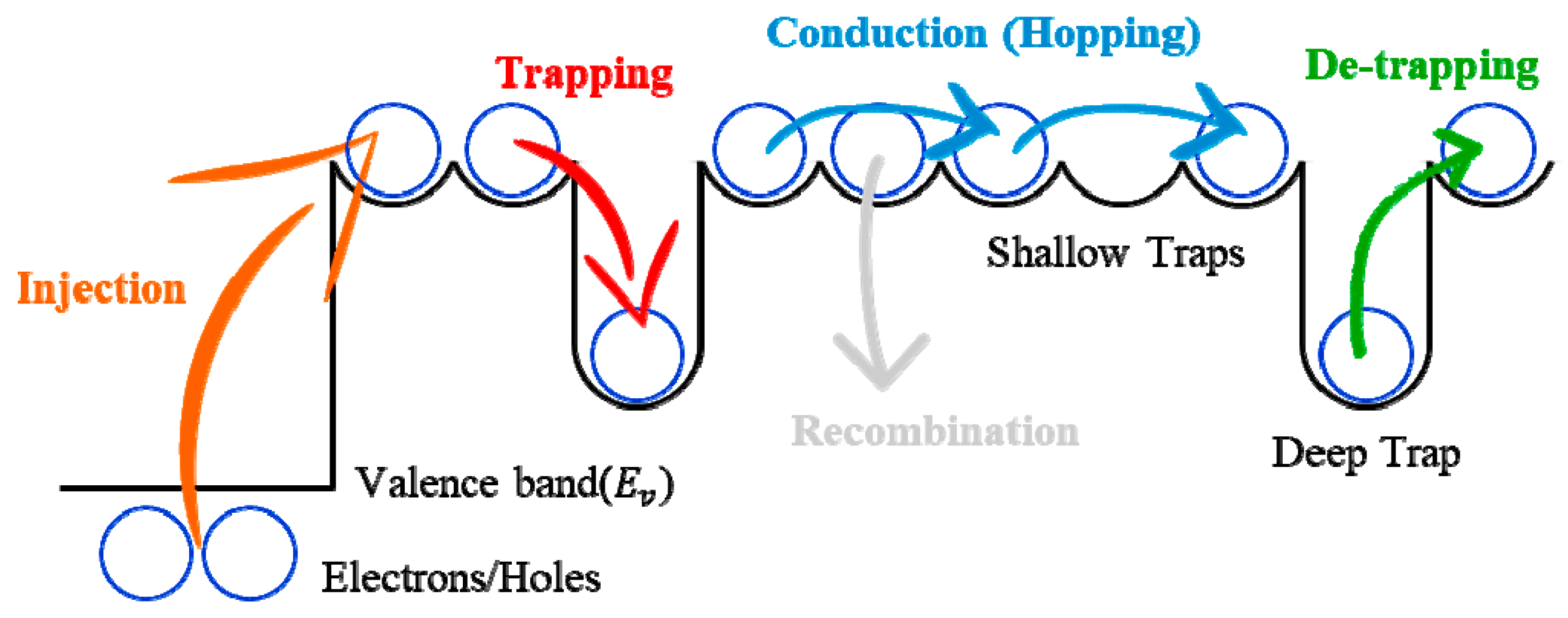
The BCT model used in this paper can not only overcome the aforementioned limitations, but realistically emulate the actual charge transport mechanism in the polyethylene-based insulation material as well. The BCT model consists of five charge transport processes: injection, conduction, trapping, detrapping, and recombination. These five processes are based on four types of carriers in the dielectric: mobile electrons, mobile holes, trapped electrons, and trapped holes. Figure 1 shows an overall schematic diagram. When the HVDC voltage is applied, the polyethylene-based dielectric is subjected to electrical stress, which results in charge injection at the interface between electrode and dielectric. Thereafter, the injected charges become mobile carriers, and the BCT process begins.
Mobile carriers travel from injected electrode to the opposite electrode. This is the conduction process which is based on hopping mechanism. The hopping mechanism means that mobile carriers hop over the shallow traps. However, not all mobile carriers can reach the counter electrode, because some of them may get trapped in deep traps during the transport. These trapped charge carriers may stay conserved in the deep trap or join the conduction process again by detrapping. Furthermore, recombination between electrons and holes can occur. Recombined neutrons cannot affect the space charge dynamics because they are no longer charge carriers.
3. Application of Bipolar Charge Transport Model to Switching Impulse Superimposed on Prestressed DC Voltage
3.1. Governing Equations
All the equations used in the BCT model written below are described in the references [9,10,11,12,13]. The BCT model dealing with transport of injected charge carriers through polyethylene-based insulation material is governed by the following equations: transport Equation (1), current continuity Equation (2), differential Equation (3), Poisson’s Equation (4), and total space charge density (5):
where ji is the transport current density associated with elementary charge q, each kind of effective mobility μi, density ni, and applied electric field E. ρ is the total space charge density.
The term Si represents the source, which denotes changes in local density due to processes other than transport, such as the internal generation and loss of charges and recombination. The changes in local density due to trapping, detrapping, and recombination processes, are expressed by Equation (6):
where coefficients Ri are the recombination coefficients, for example, Re,htr represents recombination of mobile electrons and trapped holes. Ti are trapping coefficients for electrons or holes, Ni are the trap densities for electrons or holes, and Di are the detrapping coefficients for electrons or holes, which can be expressed as follows:
where kB is Boltzmann’s constant, h is Planck’s constant, and T is the temperature inside the dielectric. In the detrapping coefficient, wi indicates detrapping barrier height, and v represents the attempt to jump frequency (i.e., the number of times per second that the trapped electron or hole strikes the ‘walls’ of the trap).
In the BCT model, we have supposed that charge generation results from injection at the electrodes according to a Schottky law given in Equation (8), for electrons and holes, respectively:
where wei and whi mean the injection barriers of electrons and hole, respectively, and A is the Richardson constant. When electrical stress exceeds the injection barrier height, charge carriers can be injected at an interface between an electrode and a dielectric. In addition, as the electric field intensity increases, at the anode or cathode where injection occurs, the barrier height lowers and the charge injection can occur easily.
The model parameters and other quantities in all equations related to mobile electrons and holes, and trapped electrons and holes, are represented by the subscripts e and h, etr and htr, respectively.
3.2. Simulation Conditions
LDPE thickness and DC input voltage were set to 50 μm and 1.5 kV, respectively, to obtain an initial electric field experienced by LDPE as 30 kV/mm. Applied DC voltage was maintained for 1·105 s to reach DC steady state. After that, the switching impulse was superimposed on prestressed DC voltage. The switching impulse is a standard waveform of 250/2500 us, with magnitude equal to that of the DC input voltage. In other words, a switching impulse with peak of 1.5 kV was additionally superimposed on DC steady state.
Simulation parameters are summarized in Table 1. To compare the effect of temperature on space charge behavior and electric field distribution, the temperature was set as 20, 40, and 60 °C. As the temperature increased, the mobility of the electron and hole also increased, and these values were derived from the experimental studies [14]. Furthermore, it is known that the electron mobility is about 10 times larger than hole mobility [15,16]. The detrapping barrier heights were also applied with the values commonly used for LDPE [17,18], and it was set to have a higher value as the temperature increased [14]. In the case of the deep trap density, the same values were applied regardless of temperature conditions [19,20]. The recombination coefficient and the relative permittivity were the same regardless of temperature condition [20]. Also, the same values were applied to the Schottky injection barriers of both anode and cathode to assume that the same amount of charge was initially injected at both electrodes. As a result, the reliability of the parameters proposed in Table 1 has been verified from experimental studies. The temperatures considered in the experimental investigation were adopted as a simulation condition. Therefore, this study did not take any linear approximation for smooth convergence, which improved the reliability of the simulation results.
3.3. Simulation Method Based on Coupling of Multisystems
To implement the BCT model, a simulation system with adequate architecture is necessary. In this work, all simulations were performed using COMSOL Multiphyiscs only. The system consists of coupled physical modules, Finite Element Method (FEM) solver, and solution store, under each type of voltage source. In the case of multiple voltage sources such as switching impulse superimposed on the DC voltage, the multisystems are necessary as shown in Figure 2. The multisystems should be solved by the combination of several modules such as electrostatic modules, transport of diluted species modules, and PDE modules. Especially, the multisystems (i.e., one containing the solution of pure DC voltage and another containing the switching impulse) have to be correctly coupled using the following process.
- Each system should be properly configured according to different independent voltage sources. In particular, the system dealing with switching impulse should have much narrower time scale than the other system due to very short duration.
- For accurate and proper coupling, strict time steps should be taken by the solver. Also, multisystems have to solve the coupled physical model for the point where the switching impulse is superimposed on the DC voltage because they have independent voltage sources (i.e., constant DC voltage and switching impulse).
- At the same time, the various continuities for the two phenomena should be taken into consideration. Most importantly, all initial values of the system that deals with the switching impulse should be the same as those under the DC steady state.
4. Simulation Results and Discussions
4.1. Space Charge Behavior under DC Stress Only
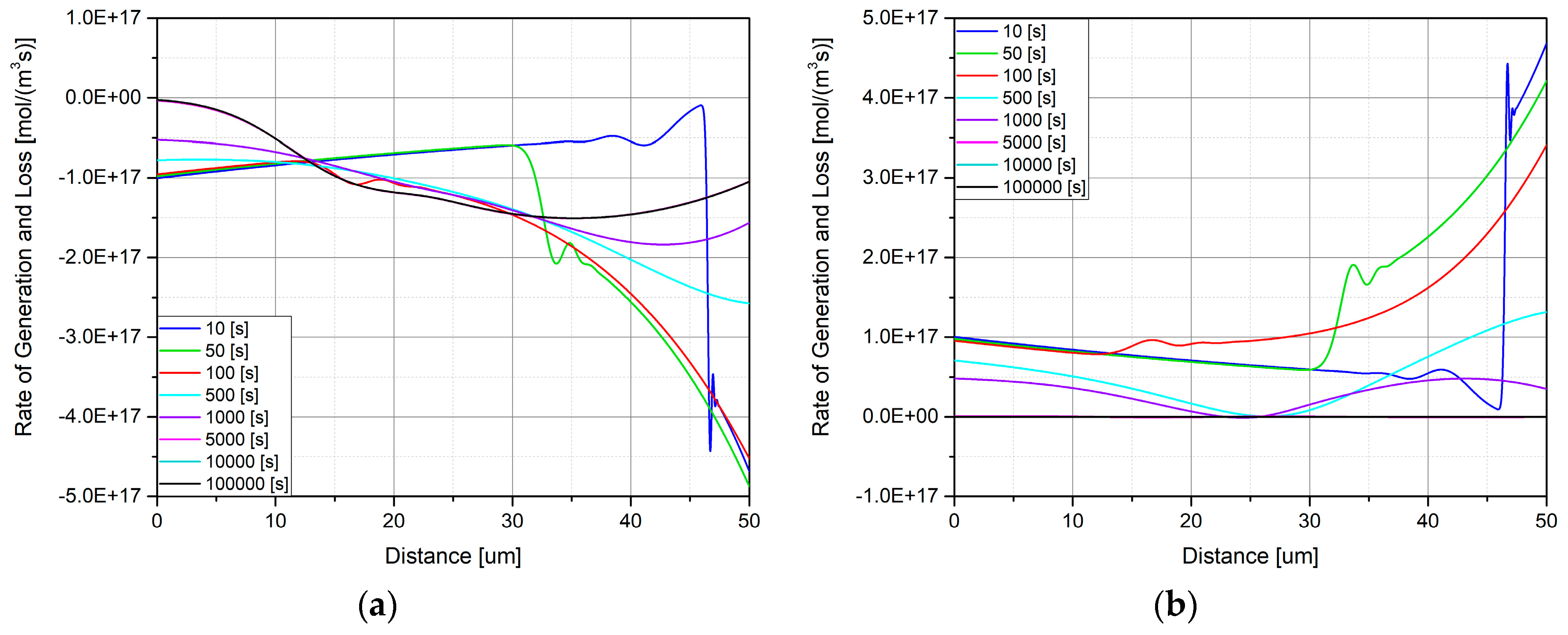
Figure 3 shows the rates of generation and loss of charge carriers at room temperature under DC voltage stress only. The horizontal axis of the graph represents the thickness of LDPE, where zero is the cathode side. The positive and negative rate on the vertical axis denotes the generation and loss of charge carriers, respectively.
For the mobile carriers, loss was significant. In the case of the mobile electrons shown in Figure 3a, it could be confirmed that they reached the anode, the counter electrode, only after about 100 s. So, the loss occurred entirely within the LDPE by reaching in a relatively short duration. Near the cathode side, which is the electron-injecting electrode, the rate of loss decreased gradually with time, and after reaching the steady state, loss did not occur at all. In contrast, near the anode, the rate of loss gradually increased with time.
On the other hand, in the case of the mobile holes, as shown in Figure 3b, unlike the electrons, the loss occurred only near the anode, which is the injection electrode for mobile holes. There was no loss at all from the beginning near the cathode side. Loss occurs relatively locally around the anode, but at a much higher rate than that of mobile electrons. In conclusion, the results of both mobile carriers can be summarized as follows:
- Loss mainly occurred in both mobile electrons and holes.
- The loss of mobile electrons occurred widely within the LDPE, while that of mobile holes occurred only near the anode, which is the injection electrode.
- The rate of loss of mobile holes is relatively high compared to that of mobile electrons.
Generations of trapped carriers usually occurred. This is because that loss of mobile carriers is the source of trapping. In the case of the trapped electrons shown in Figure 3c, the generation occurred entirely within the LDPE. Near the cathode side, which is the injection electrode of mobile electrons, the generation rates decreased gradually. These results indicate that rate distribution of generation of trapped electrons and loss of mobile electrons is symmetrical along the horizontal axis.
As shown in Figure 3d, the trapped holes are also symmetrical about the horizontal axis because the mobile and trapped holes are closely related. In conclusion, the results of both trapped carriers can be summarized as follows:
- Both trapped electrons and holes were mainly generated, in contrast to the mobile carriers.
- The generation of trapped electrons occurred throughout the LDPE, whereas that of trapped holes occurred only near the anode, the injection electrode of holes.
- The rate of generation of trapped holes is relatively high compared to that of trapped electrons.
These rates of generation and loss can be explained by bipolar charge transport mechanisms such as trapping, detrapping, and recombination. For the mobile carriers, only detrapping corresponds to generation, while trapping and recombination correspond to loss. The conduction process describes the hopping of mobile carriers, but does not affect generation and loss. Loss mainly occurred in mobile carriers. Thus, it indicates that trapping and recombination are far more dominant than detrapping in mobile carriers.
On the other hand, the difference between mobile electrons and mobile holes was significant. The mobile holes concentrated near the anode, while the mobile electrons were distributed relatively uniformly throughout the LDPE. This is due to the difference in effective mobility of the two carriers. The electron mobility is approximately ten times larger than hole mobility. Due to higher mobility of electrons, the loss of mobile electrons occurred across the volume of the LDPE, but at a much lower rate than the holes.
For trapped carriers, in contrast to mobile carriers, only trapping corresponds to generation, and detrapping and recombination correspond to loss. Since recombination means neutralization, it is always considered as a loss, regardless of the carrier type, whether it is the mobile carrier or trapped one. Therefore, the relationship between generation and loss of carriers can be summarized as shown in Table 2. Total rates in mobile and trapped carriers were distributed symmetrically along the horizontal axis. Nevertheless, the distribution is not perfectly symmetrical due to recombination. In other words, the generation for one side may not be the loss for the other, since recombination is always a loss regardless of the carrier type. This is particularly noticeable in Figure 3a,c. Near the anode, the loss of the mobile electrons did not completely coincide with the generation of the trapped electrons. This is considered to be due to the vigorous recombination process at that place.
Figure 4 and Figure 5 show the rates of generation and loss under different temperature conditions. The effects due to different mobility, dominance of trapped carriers relative to mobile carriers, and dominance of holes relative to electrons were similar to those at room temperature. The difference of charge transport characteristics according to temperature condition can be summarized as follows:
- As the temperature increases, the effective mobility also increases, so the rate of generation and loss is less localized at higher temperature condition compared to that at room temperature, especially in holes. It could be confirmed by the fact that the trapped holes near the anode shown in Figure 4b and Figure 5b are relatively less localized than those at room temperature. This is due to higher mobility.
- However, the overall rate has increased significantly, resulting in more vigorous generation and loss under high temperature conditions. This is closely related to space charge dynamics, and it can lead to the further distortion of electric field distribution.
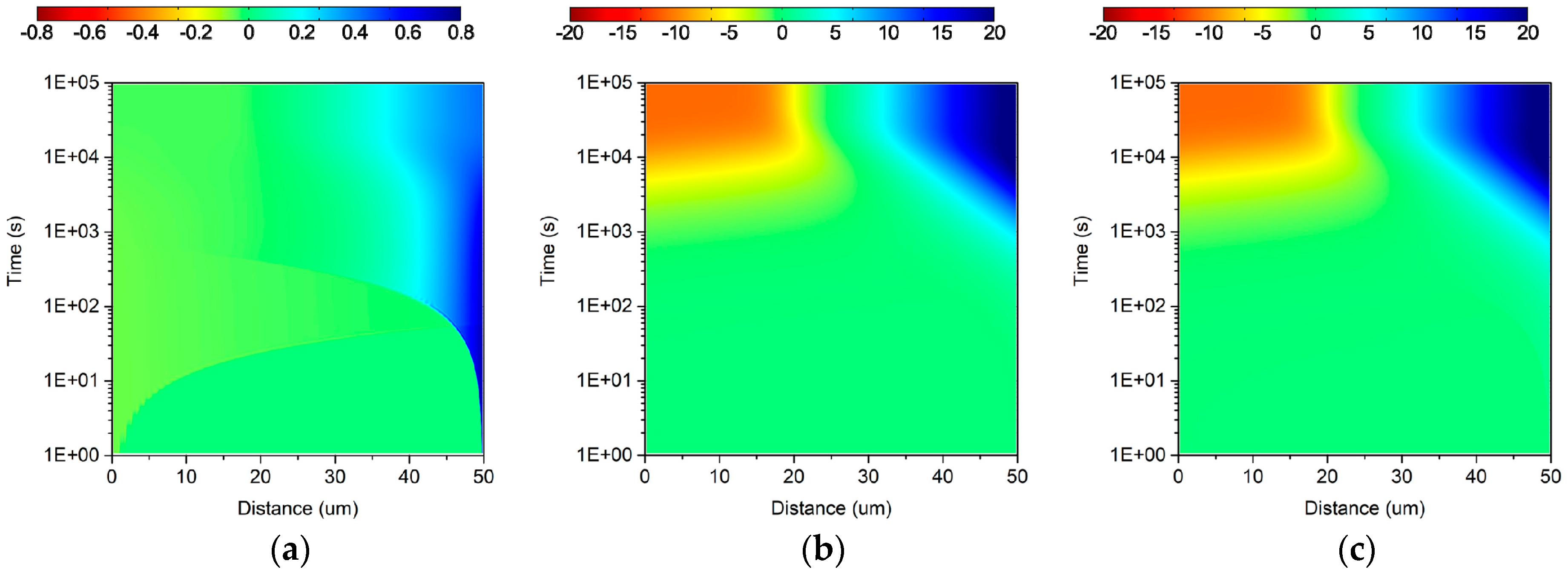
Figure 6, Figure 7 and Figure 8 represent the mobile and trapped charge density, and total charge density at different temperature conditions. Left and right sides of the horizontal axis represent the cathode and the anode, respectively. The vertical axis denotes time, which is expressed as a log scale. Positive and negative color legends represent charge density of holes and electrons, respectively. Note that the ranges of scales represented by color legends are different.
As shown in Figure 6a, both mobile carriers stood out early in the DC voltage application at room temperature, but decreased gradually after that. Especially, the generation of the mobile holes was relatively noticeable. The density of trapped carriers increased significantly after 1 × 10³ s, as shown in Figure 6b. This is because the mobile carriers generated by the injection in the early stage were trapped near the injected electrode and could not reach the opposite electrode. Therefore, density of trapped electrons increased near the cathode and that of trapped holes increased near the anode. Furthermore, Figure 6c shows that most of the total charge density is represented by trapped carriers, and the distribution was similar to trapped charge density.
It implies that the trapping has the most significant influence on the space charge distribution. At the same time, electron distribution was relatively uniform, whereas holes were concentrated near the anode. This results from the different effective mobility of electrons and holes. In other words, the effective mobility of charge carriers also plays a significant role in the space charge dynamics.
We can conclude the following from the results in Figure 6. The dominant carriers determining the space charge distribution are trapped carriers, not the mobile carriers. Furthermore, the space charge behavior is governed by holes, rather than electrons. As a result, a homocharge distribution was formed in the LDPE, and it was consistent with some experimental reports [21,22,23].
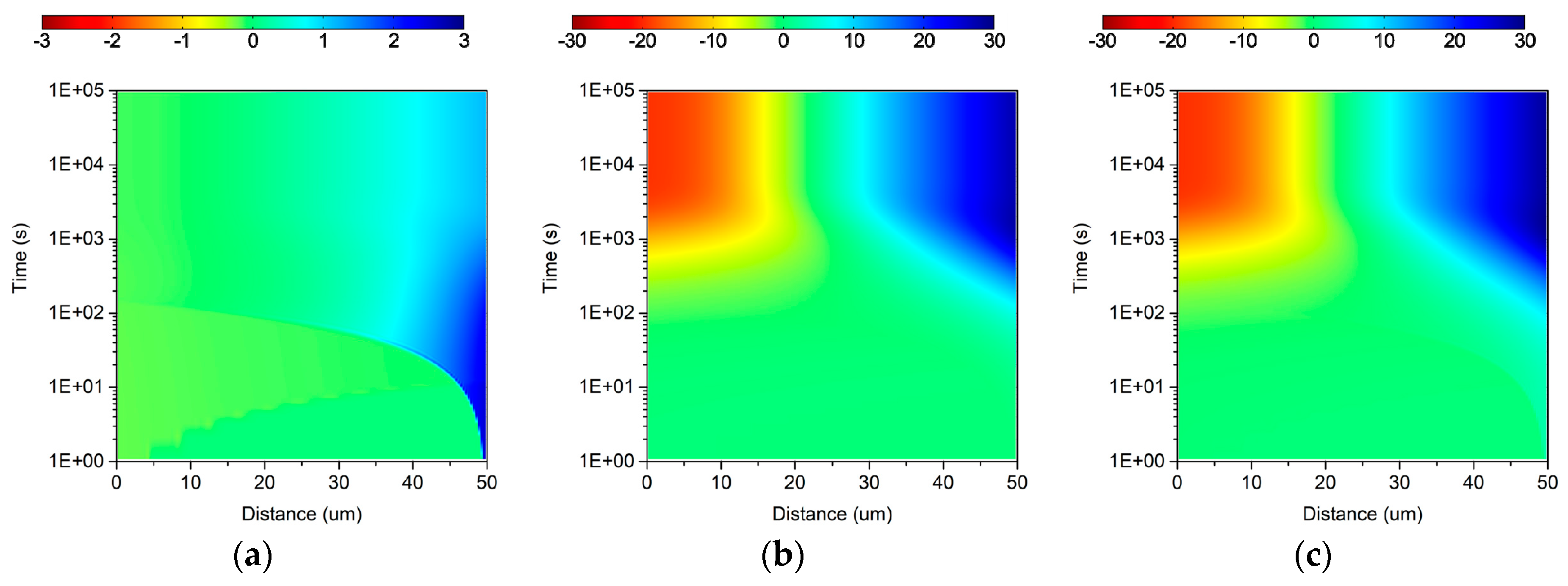
Figure 7 and Figure 8 show the space charge density under different temperature conditions. As temperature increased, space charge density became more pronounced around both electrodes. It began to accumulate from an earlier time and reached a steady state relatively quickly. In the case of 60 °C shown in Figure 8c, total space charge began to accumulate relatively early and its density doubled compared to that at 20 °C shown in Figure 6c. However, it should be noted that trapped carriers and holes remained dominant even at higher temperatures.
4.2. Space Charge Behavior under Switching Impulse Superimposed on Prestressed DC Voltage
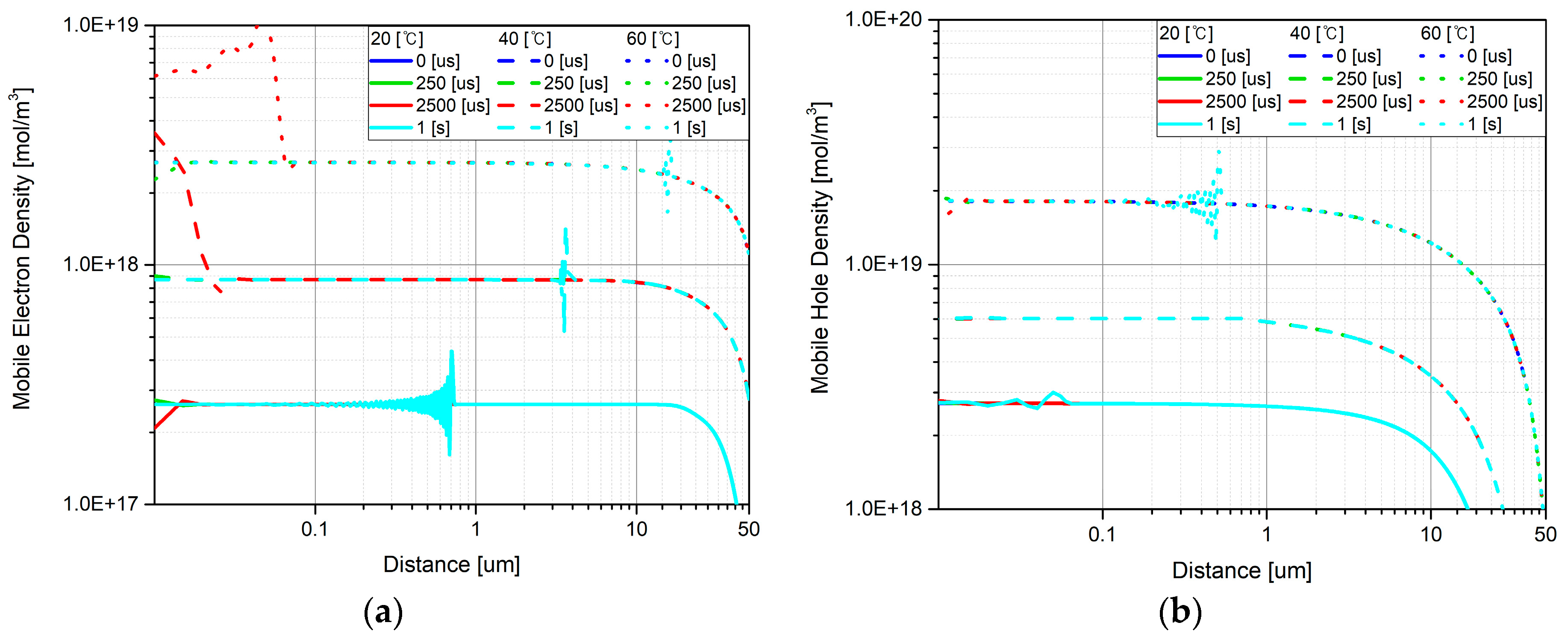
Figure 9 shows densities of mobile carriers immediately after the switching impulse is superimposed on prestressed DC voltage. Figure 9a,b show the density of mobile electrons and mobile holes, respectively, while closer to zero on the horizontal axis means closer to the cathode or the anode. Temperatures 20, 40, and 60 °C are represented by solid, dash, and dot lines, respectively; 0 μs and 1 s denote the mobile carriers’ density under DC voltage before and after switching impulse superposition, respectively. In addition, 250 and 2500 μs indicate the time to peak of superimposed switching impulse and the time to half of the peak value, respectively. They are presented in different colors such as blue, green, red, and cyan according to time.
In Figure 9a, the higher the temperature, the higher the mobile electron density will be. High temperature not only causes high effective mobility but also increases the trapping coefficient. This leads to higher conduction and trapping as well. Therefore, mobile carriers can reach the opposite electrode quickly or trapping can occur rather easily. The homocharge can be reduced by transporting and trapping mobile carriers near the injected electrode. However, since the amount of injected charge is also large, the density of mobile carrier can be increased near the injection electrode.
The distribution of mobile holes density is shown in Figure 9b, and it is also similar to that of mobile electrons density. However, it was slightly denser than mobile electrons density, which was because the mobility of the holes was relatively low at all temperature conditions. Thus, the mobile holes did not leave noticeably from the anode side, and this caused an increase in mobile holes density.
The number of mobile carriers injected at the electrode increased instantaneously due to lowered injection barrier height caused by an increase in externally applied electric field. However, as mentioned above, the share of mobile carriers in space charge density is meagre, and due to short duration of switching impulse, trapping fails to occur. As soon as the electrical stress was removed, it returned to its original DC steady state.
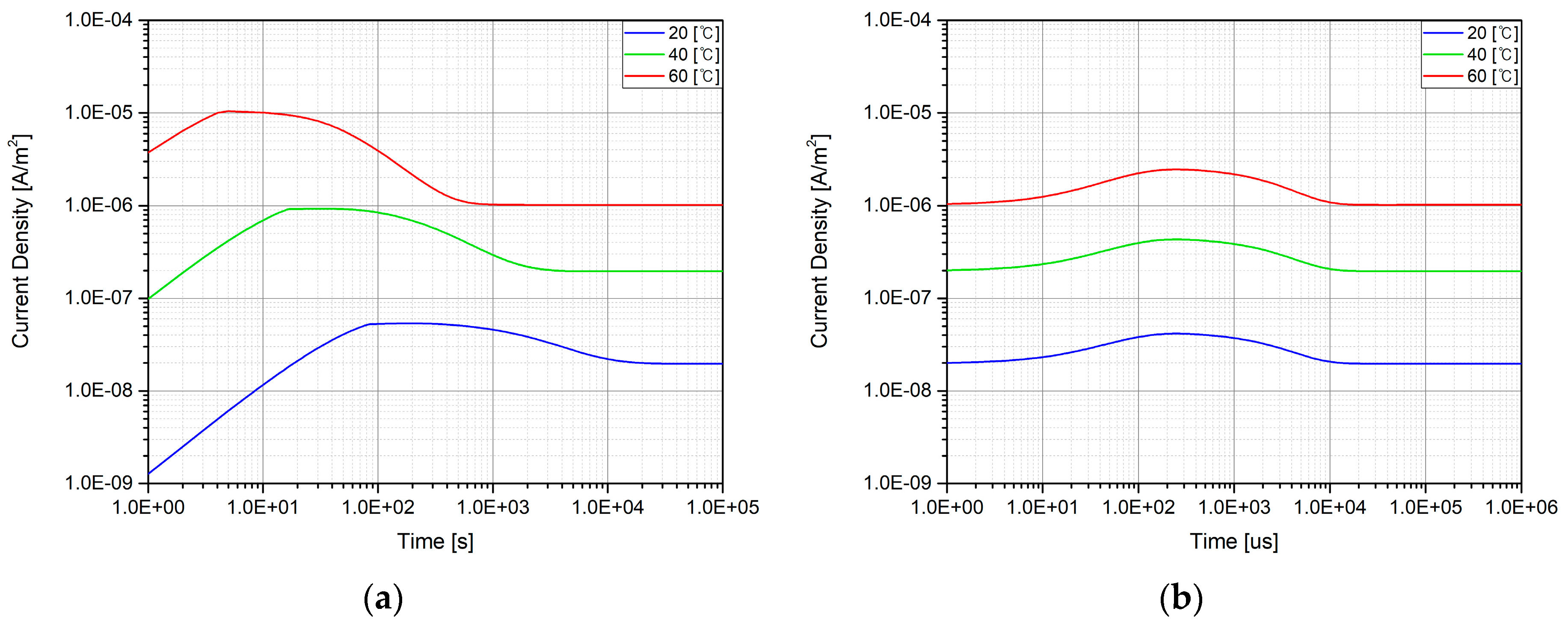
It could be also confirmed by a time-varying current density which could be obtained by the following Equation (9). The current density distribution before and under switching impulse superimposed on prestressed DC voltage are shown in Figure 10a,b, respectively.
As shown in Figure 10a, the current density under DC voltage was relatively high at elevated temperature conditions. This was in line with the mobile charge density shown in Figure 9. This is because the current density is based on transport of the mobile carriers. As explained above, the higher amount of injected charge at high temperature eventually promotes the hopping process, further increasing the conduction current. In addition, higher temperature allowed reaching DC steady state earlier. This was in line with the space charge distribution shown in Figure 6, Figure 7 and Figure 8, which was related to a time constant [24]. The increase of effective mobility caused the rise of the electrical conductivity, which resulted in reduced time constant and reaching the steady state within a short duration.
Figure 10b shows the current density under switching impulse superimposed on prestressed DC voltage. The current density was temporarily increased at the moment when the switching impulse was superimposed. Thereafter, it returned to DC steady state as soon as the switching impulse was removed. As a result, the switching impulse did not have any effect on space charge dynamics and, consequently, neither did the short duration switching impulse have a lasting impact on space charge behavior. Temperature condition also appeared to have no influence on the space charge distribution.
4.3. The Effect of Superposition on Electric Field Distribution
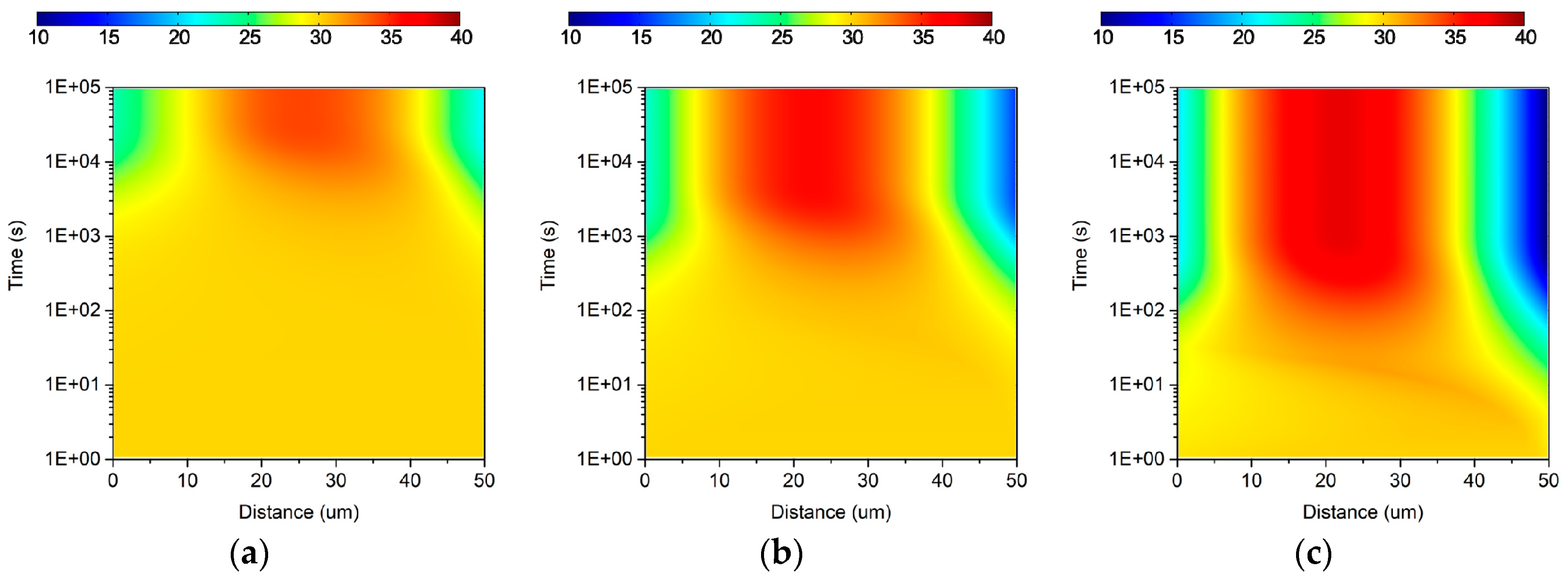
Figure 11 shows the DC electric field distribution under DC stress only. The left and right sides of the horizontal axis represent the cathode and the anode, respectively. The vertical axis represents time, which is expressed as a log scale. The same legend of 10–40 kV/mm is presented for easy comparison. Figure 11a–c show the results in 20, 40, and 60 °C, respectively.
As the temperature increased, not only did the field distortion initiate earlier, but also the distortion became extreme. Also, the electric field distortion on the anode side was relatively more prominent, which was influenced by the dominance of trapped holes due to slow mobility. As a result, the maximum electric field intensity occurred in the middle of the LDPE due to homocharge distribution under all temperature conditions, and the maximum electric field intensity also increased with increasing temperature.
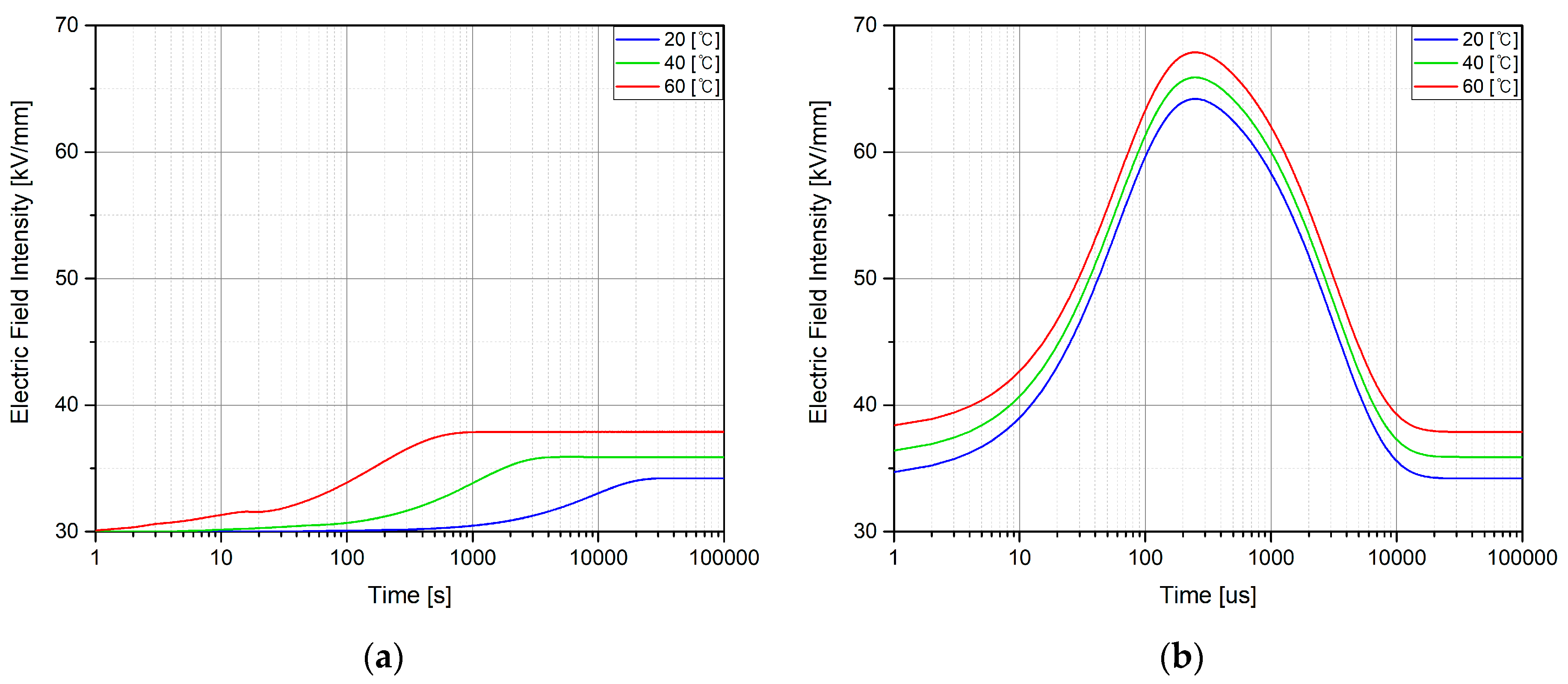
Figure 12 is presented to compare an electric field intensity with a switching impulse superposition. Figure 12a,b show the change of the time-varying field intensity under DC voltage only and under switching impulse superimposed on DC voltage, respectively. For easy comparison, the range of the vertical axis for the electric field intensity was set the same.
In the case of the electric field intensity under DC voltage only, as mentioned above and as shown in Figure 12a, higher temperature increases the maximum field intensity by causing significant electric field distortion. In Figure 12b, the maximum electric field intensities under switching impulse superimposed on prestressed DC voltage were just increased by 30 kV/mm regardless of the temperature. This increased intensity was just caused by the increased potential difference as a result of superposition. Thereafter, it returned to electric field intensity at DC steady state.
As a result, the final field intensity was determined by the vector sum of the instantaneous capacitive field due to the switching impulse and the lasting resistive field intensity under the DC voltage. This means that the electric field distribution under the DC voltage before superposition can also have a considerable influence on the determination of the electric field distribution under switching impulse superposition.
Table 3 shows the maximum electric field intensity according to simulation condition. Firstly, we evaluated the increase in maximum intensity in DC steady state compared to the initial intensity. The initial field value was set to 30 kV/mm regardless of temperature depending on the simulation conditions of applied DC voltage. However, as duration of DC voltage application increased, electric field distorted. The maximum field intensities were 34.2, 35.9, and 37.9 kV/mm at temperature conditions of 20, 40, and 60 °C, respectively. These values mean that they increased about 14.0, 19.7, and 26.3%, respectively, compared with the initial field intensities. From the simulation results, the higher the temperature, the higher the maximum field intensity and the greater the distortion of the electric field.
On the other hand, since the switching impulse superposition does not affect the space charge behavior, instantaneously increased potential difference only had a prominent effect on electric field distribution. When the temperature conditions were 20, 40, and 60 °C, the maximum intensities were 64.2, 65.9, and 67.9 kV/mm, respectively. These values were the maximum field intensities at 250 μs after the switching impulse was superimposed on DC voltage. As a result, the maximum electric field intensity under the switching impulse superimposed on prestressed DC voltage increased 87.7% compared to the DC steady state. In the case of 40 and 60 °C, the increase was 83.6 and 79.2%, respectively.
In conclusion, it should be noted that although switching impulse does not cause space charge to redistribute, the electrical stress is enhanced significantly. This enhancement in electric field can lead to a significant increase in the probability of dielectric breakdown.
5. Conclusions
The effect of same polarity switching impulse superposition on an electric field distribution under DC steady state was discussed considering space charge dynamics. The following can be concluded from this study.
- In the case of application of HVDC voltage, the increase in charge accumulation was higher at high temperatures.
- Trapped carriers and holes rather than mobile carriers and electrons are more significant in determining the space charge behaviors.
- The switching impulse had no influence on space charge distribution. Because of its momentary nature, switching impulse does not influence the charge transport process.
- However, a superimposed switching impulse raised the maximum electric field intensity by up to 87.7% compared to the DC steady state.
The simulation method established in this work can be used to study many emerging issues in the future. Firstly, the space charge dynamics and electric field distribution in real-size HVDC cable insulation during transient state can be studied. Additionally, the effects of variation of polarity and magnitude of superimposed switching impulse on the insulating material can be investigated.
Author Contributions
I.-S.K. conceptualized the topic, formulated methodology, performed simulations, and prepared an original draft; M.A. performed a formal analysis and reviewed the draft; S.-J.K. curated the data and edited the draft; B.-W.L. supervised the study.
Funding
This research received no external funding.
Acknowledgments
This work was supported by the Ministry of Trade, Industry, and Energy of Korea through the Human Resources Program in Energy Technology of the Korea Institute of Energy Technology Evaluation and Planning (KETEP) under Grant 20174030201780 and by Korea Electric Power Corporation (Grant number: R17XA05-3).
Conflicts of Interest
The authors declare no conflict of interest.
References
- Wang, H.T.; Cao, J.Z.; He, Z.Y.; Yang, J.; Han, Z.Y.; Chen, G. Research on Overvoltage for XLPE Cable in a Modular Multilevel Converter HVDC Transmission System. IEEE Trans. Power Deliv. 2016, 31, 683–692. [Google Scholar] [CrossRef]
- CIGRE, T. Recommendations for testing DC extruded cable systems for power transmission at a rated voltage up to 500 kV. 2012. Available online: https://e-cigre.org/publication/496-recommendations-for-testing-dc-extruded-cable-systems-for-power-transmission-at-a-rated-voltage-up-to-500-kv---------this-tb-replaces-tb-219 (accessed on 14 May 2019).
- Current, H.V.D. Power Transmission–Cables with Extruded Insulation and Their Accessories for Rated Voltages up to 320 kV for Land Applications–Test Methods and Requirements. Comitte Draft, CD IEC 2014, 62895. Available online: https://webstore.iec.ch/publication/34020 (accessed on 14 May 2019).
- Zhou, C.; Chen, G. Space charge behaviours in polyethylene under combined AC and DC electric fields. In Proceedings of the 2014 IEEE Conference on Electrical Insulation and Dielectric Phenomena (CEIDP), Des Moines, IA, USA, 19–22 October 2014; pp. 848–851. [Google Scholar]
- Le Roy, S.; Segur, P.; Teyssedre, G.; Laurent, C. Description of bipolar charge transport in polyethylene using a fluid model with a constant mobility: Model prediction. J. Phys. D Appl. Phys. 2004, 37, 298–305. [Google Scholar] [CrossRef]
- Neyts, K.; Karvar, M.; Drobchak, O.; Brans, T.; Strubbe, F.; Beunis, F. Simulation of charge transport and steady state in non-polar media between planar electrodes with insulating layers. Colloid Surface A 2014, 440, 101–109. [Google Scholar] [CrossRef]
- Banda, M.; Griseri, V.; Teyssedre, G.; Le Roy, S. Modelling Charge Generation and Transport in Low Density Polyethylene Irradiated by an Electron-Beam. In Proceedings of the 2018 IEEE 2nd International Conference on Dielectrics (ICD), Budapest, Hungary, 1–5 July 2018; pp. 1–4. [Google Scholar]
- Min, D.M.; Li, S.T. A Comparison of Numerical Methods for Charge Transport Simulation in Insulating Materials. IEEE Trans. Dielectr. Electr. Insul. 2013, 20, 955–964. [Google Scholar] [CrossRef]
- Belgaroui, E.; Boukhris, I.; Kallel, A.; Teyssedre, G.; Laurent, C. A new numerical model applied to bipolar charge transport, trapping and recombination under low and high dc voltages. J. Phys. D Appl. Phys. 2007, 40, 6760–6767. [Google Scholar] [CrossRef]
- Teyssedre, G.; Laurent, C. Charge transport modeling in insulating polymers: From molecular to macroscopic scale. IEEE Trans. Dielectr. Electr. Insul. 2005, 12, 857–875. [Google Scholar] [CrossRef]
- Baudoin, F.; Le Roy, S.; Teyssedre, G.; Laurent, C. Bipolar charge transport model with trapping and recombination: An analysis of the current versus applied electric field characteristic in steady state conditions. J. Phys. D Appl. Phys. 2008, 41. [Google Scholar] [CrossRef]
- Poplavskyy, D.; Su, W.C.; So, F. Bipolar charge transport, injection, and trapping studies in a model green-emitting polyfluorene copolymer. J. Appl. Phys. 2005, 98. [Google Scholar] [CrossRef]
- Hoang, A.T.; Serdyuk, Y.V.; Gubanski, S.M. Charge Transport in LDPE Nanocomposites Part II-Computational Approach. Polymers 2016, 8, 103. [Google Scholar] [CrossRef] [PubMed]
- Hoang, A.T.; Pallon, L.; Liu, D.M.; Serdyuk, Y.V.; Gubanski, S.M.; Gedde, U.W. Charge Transport in LDPE Nanocomposites Part I-Experimental Approach. Polymers 2016, 8, 87. [Google Scholar] [CrossRef] [PubMed]
- Toomer, R.; Lewis, T.J. Charge Trapping in Corona-Charged Polyethylene Films. J. Phys. D Appl. Phys. 1980, 13, 1343–1356. [Google Scholar] [CrossRef]
- Chen, G.; Tay, T.Y.G.; Davies, A.E.; Tanaka, Y.; Takada, T. Electrodes and charge injection in low-density polyethylene—Using the pulsed electroacoustic technique. IEEE Trans. Dielectr. Electr. Insul. 2001, 8, 867–873. [Google Scholar] [CrossRef]
- Fischer, P.; Rohl, P. Thermally Stimulated and Isothermal Depolarization Currents in Low-Density Polyethylene. J. Polym. Sci. Pol. Phys. 1976, 14, 531–542. [Google Scholar] [CrossRef]
- Mizutani, T.; Suzuoki, Y.; Ieda, M. Thermally Stimulated Currents in Polyethylene and Ethylene-Vinyl-Acetate Copolymers. J. Appl. Phys. 1977, 48, 2408–2413. [Google Scholar] [CrossRef]
- Tian, F.Q.; Lei, Q.Q.; Wang, X.; Wang, Y. Effect of deep trapping states on space charge suppression in polyethylene/ZnO nanocomposite. Appl. Phys. Lett. 2011, 99. [Google Scholar] [CrossRef]
- Le Roy, S.; Teyssedre, G.; Laurent, C.; Montanari, G.C.; Palmieri, F. Description of charge transport in polyethylene using a fluid model with a constant mobility: Fitting model and experiments. J. Phys. D Appl. Phys. 2006, 39, 1427–1436. [Google Scholar] [CrossRef]
- Liu, N.; He, M.; Alghamdi, H.; Chen, G.; Fu, M.L.; Li, R.H.; Hou, S. An improved model to estimate trapping parameters in polymeric materials and its application on normal and aged low-density polyethylenes. J. Appl. Phys. 2015, 118. [Google Scholar] [CrossRef]
- Han, B.; Wang, X.; Sun, Z.; Yang, J.M.; Lei, Q.Q. Space charge suppression induced by deep traps in polyethylene/zeolite nanocomposite. Appl. Phys. Lett. 2013, 102. [Google Scholar] [CrossRef]
- Khalil, M.S.; Hansen, B.S. Investigation of Space-Charge in Low-Density Polyethylene Using a Field Probe Technique. IEEE Trans. Dielectr. Electr. Insul. 1988, 23, 441–445. [Google Scholar] [CrossRef]
- Jeroense, M.J.P.; Morshuis, P.H.F. Electric fields in HVDC paper-insulated cables. IEEE Trans. Dielectr. Electr. Insul. 1998, 5, 225–236. [Google Scholar] [CrossRef] [Green Version]
Figure 1.
Overall processes of BCT model.

Figure 2.
Implementation process based on multisystems in COMSOL.
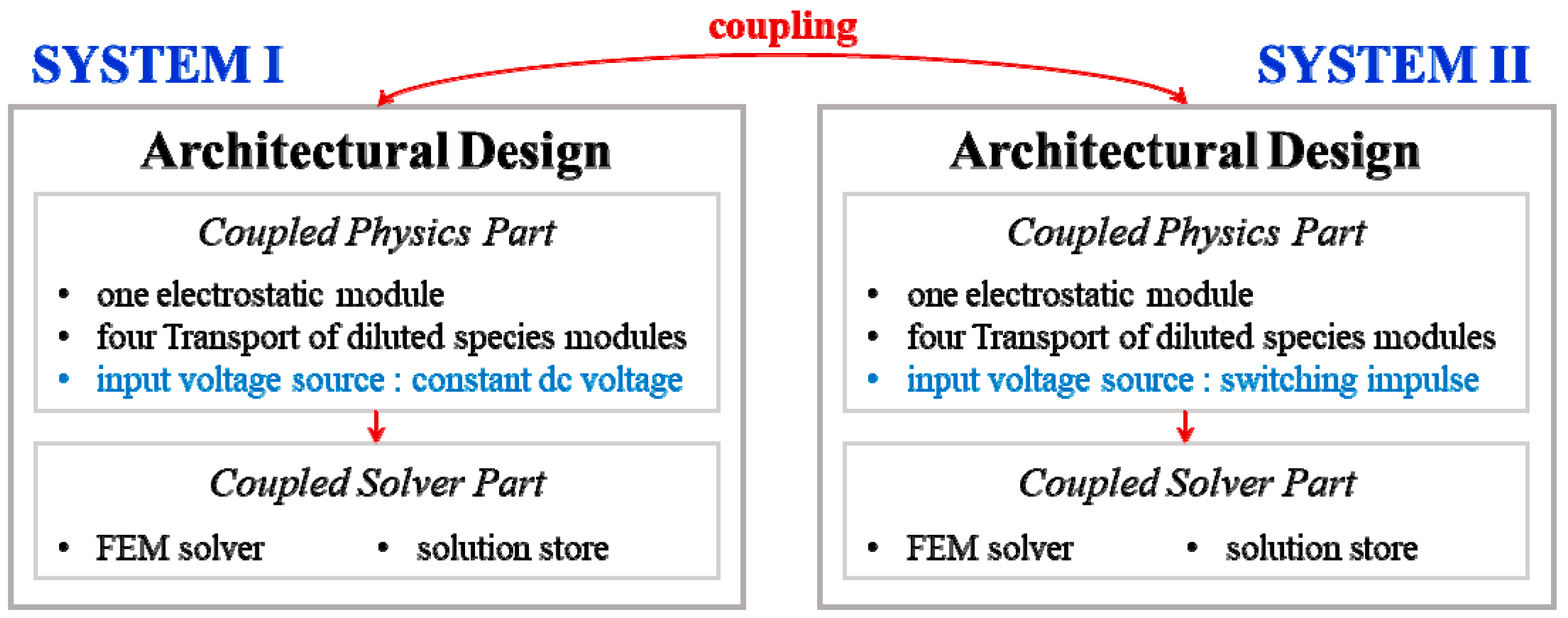
Figure 3.
Rates of generation and loss of carriers at room temperature (=20 °C): (a) mobile electrons; (b) mobile holes; (c) trapped electrons; (d) trapped holes.
Figure 3.
Rates of generation and loss of carriers at room temperature (=20 °C): (a) mobile electrons; (b) mobile holes; (c) trapped electrons; (d) trapped holes.
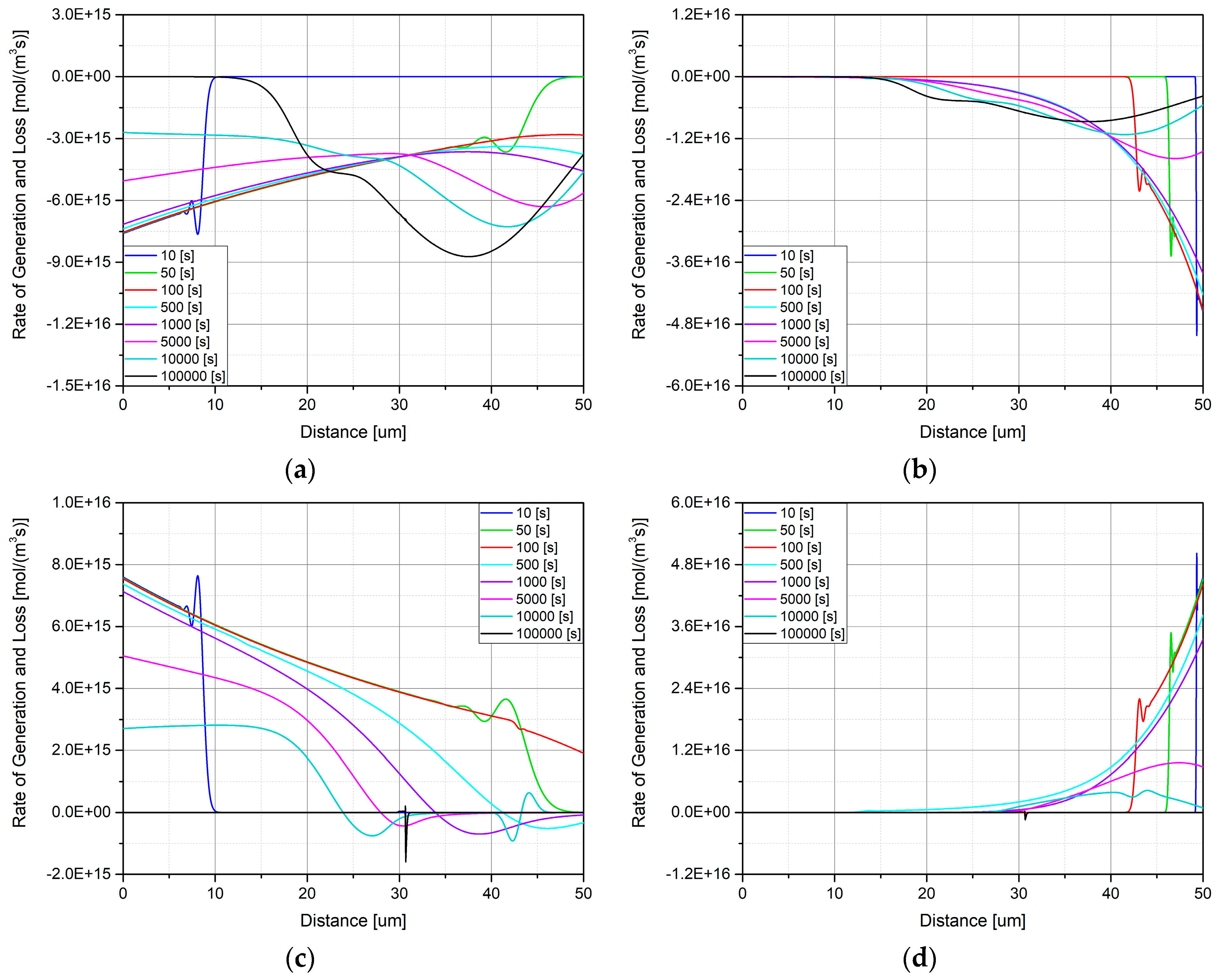
Figure 4.
Rates of generation and loss of carriers at 40 °C: (a) mobile carriers; (b) trapped carriers.
Figure 4.
Rates of generation and loss of carriers at 40 °C: (a) mobile carriers; (b) trapped carriers.

Figure 5.
Rates of generation and loss of carriers at 60 °C: (a) mobile carriers; (b) trapped carriers.
Figure 5.
Rates of generation and loss of carriers at 60 °C: (a) mobile carriers; (b) trapped carriers.
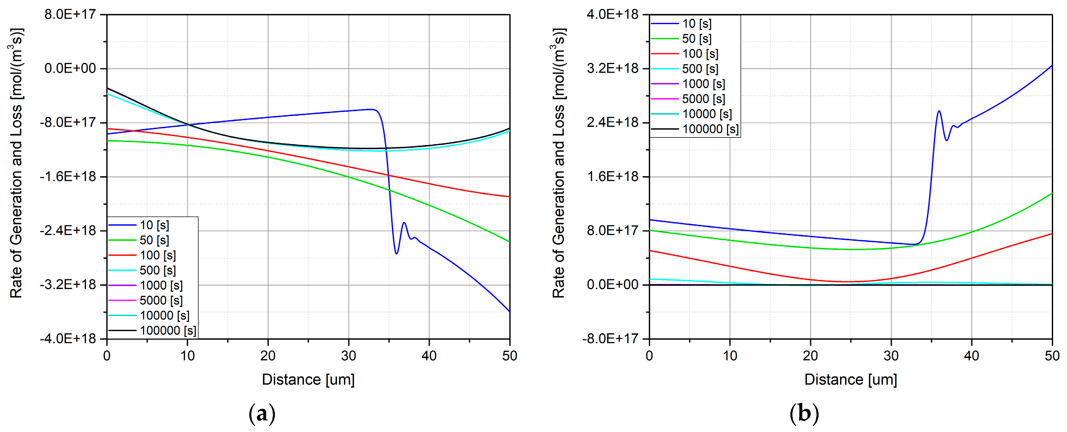
Figure 6.
Space charge distribution at room temperature (=20 °C): (a) mobile charge density (C/m3); (b) trapped charge density (C/m3); (c) total charge density (C/m3).
Figure 6.
Space charge distribution at room temperature (=20 °C): (a) mobile charge density (C/m3); (b) trapped charge density (C/m3); (c) total charge density (C/m3).

Figure 7.
Space charge distribution at 40 °C: (a) mobile charge density (C/m3); (b) trapped charge density (C/m3); (c) total charge density (C/m3).
Figure 7.
Space charge distribution at 40 °C: (a) mobile charge density (C/m3); (b) trapped charge density (C/m3); (c) total charge density (C/m3).

Figure 8.
Space charge distribution at 60 °C: (a) mobile charge density (C/m3); (b) trapped charge density (C/m3); (c) total charge density (C/m3).
Figure 8.
Space charge distribution at 60 °C: (a) mobile charge density (C/m3); (b) trapped charge density (C/m3); (c) total charge density (C/m3).
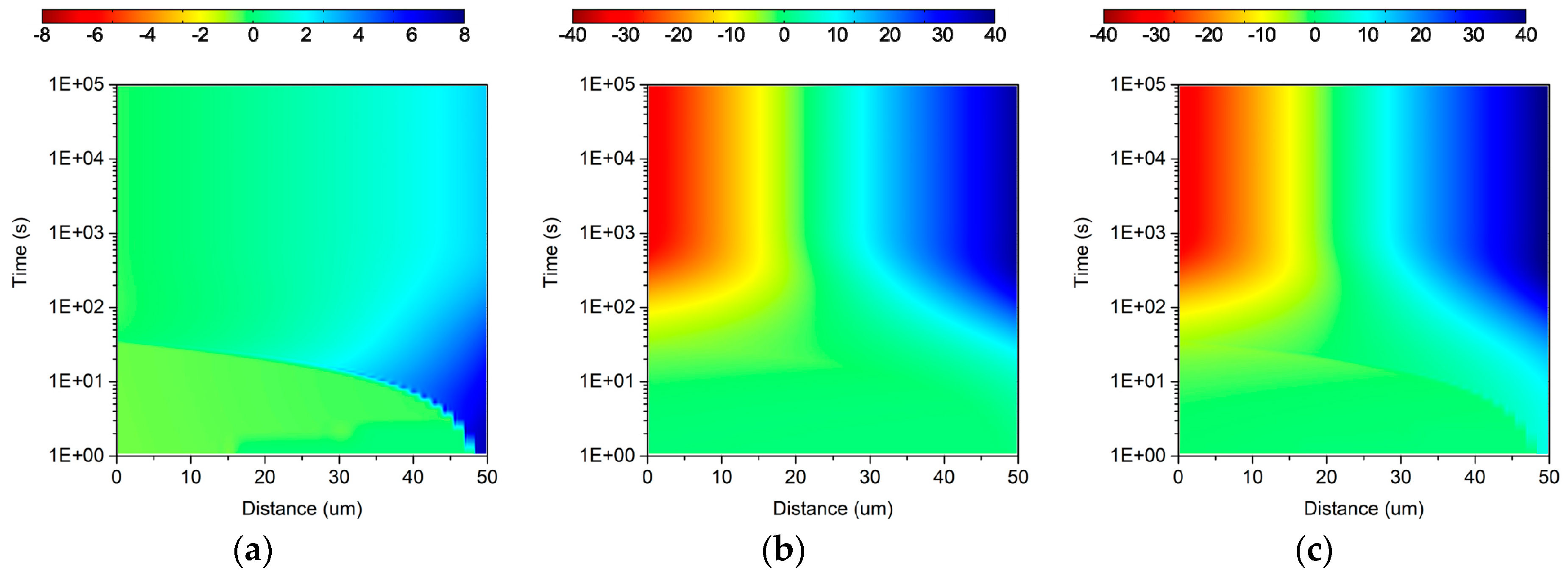
Figure 9.
Mobile carrier density immediately after switching impulse is superimposed on prestressed DC voltage: (a) mobile electrons; (b) mobile holes.
Figure 9.
Mobile carrier density immediately after switching impulse is superimposed on prestressed DC voltage: (a) mobile electrons; (b) mobile holes.

Figure 10.
Comparison of current density at different temperature conditions: (a) under DC voltage only; (b) under switching impulse superimposed on prestressed DC voltage.
Figure 10.
Comparison of current density at different temperature conditions: (a) under DC voltage only; (b) under switching impulse superimposed on prestressed DC voltage.

Figure 11.
Time-dependent electric field distribution under DC stress only at different temperature conditions: (a) electric field (kV/mm) at room temperature (=20 °C); (b) electric field (kV/mm) at 40 °C; (c) electric field (kV/mm) at 60 °C.
Figure 11.
Time-dependent electric field distribution under DC stress only at different temperature conditions: (a) electric field (kV/mm) at room temperature (=20 °C); (b) electric field (kV/mm) at 40 °C; (c) electric field (kV/mm) at 60 °C.

Figure 12.
Comparison of current density according to superposition of switching impulse at different temperature conditions: (a) under DC voltage only; (b) under switching impulse superimposed on prestressed DC voltage.
Figure 12.
Comparison of current density according to superposition of switching impulse at different temperature conditions: (a) under DC voltage only; (b) under switching impulse superimposed on prestressed DC voltage.


| Parameters | Symbols | Units | Temperature (°C) | ||
|---|---|---|---|---|---|
| 20 | Parameters | Symbols | |||
| Effective Mobility | μe | m2/(V·s) | 3.0 × 10⁻¹⁴ | 1.5 × 10⁻¹³ | 5.5 × 10⁻¹³ |
| μh | 2.5 × 10⁻¹⁵ | 1.2 × 10⁻¹⁴ | 5.0 × 10⁻¹⁴ | ||
| Trapping Coefficients | te | 1/s | 0.02 | 0.08 | 0.25 |
| th | 0.01 | 0.03 | 0.08 | ||
| Detrapping Barrier Height | wtre | eV | 0.93 | 0.96 | 1.00 |
| wtrh | 0.93 | 0.96 | 1.00 | ||
| Deep Trap Density | Netr | C/m3 | 100 | 100 | 100 |
| Nhtr | 100 | 100 | 100 | ||
| Recombination Coefficients | Reh | m3/s | 0 | 0 | 0 |
| Rehtr | 6.4 × 10⁻²² | 6.4 × 10⁻²² | 6.4 × 10⁻²² | ||
| Retrh | 6.4 × 10⁻²² | 6.4 × 10⁻²² | 6.4 × 10⁻²² | ||
| Retrhtr | 6.4 × 10⁻²² | 6.4 × 10⁻²² | 6.4 × 10⁻²² | ||
| Relative Permittivity | εr | 1 | 2.3 | 2.3 | 2.3 |
| Schottky Injection Barrier Height | wei | eV | 1.20 | 1.20 | 1.20 |
| whi | 1.20 | 1.20 | 1.20 | ||
Table 2.
Mechanism of generation and losses of charge carriers.
| Rate | Mobile Carriers | Trapped Carriers |
|---|---|---|
| Generation | Detrapping | Trapping |
| Loss | Trapping, recombination | Detrapping, recombination |
Table 3.
Summary of maximum electric field intensity according to simulation condition.
| Electric Field Intensity | Unit | Temperature (°C) | ||
|---|---|---|---|---|
| 20 | 40 | 60 | ||
| EINITIAL | kV/mm | 30.0 | 30.0 | 30.0 |
| EDC.MAX | kV/mm | 34.2 | 35.9 | 37.9 |
| EDC.MAX+SI | kV/mm | 64.2 | 65.9 | 67.9 |
| Increased % of EDC.MAX compared to EINITIAL | % | 14.0 | 19.7 | 26.3 |
| Increased % of EDC.MAX+SI compared to EDC.MAX | % | 87.7 | 83.6 | 79.2 |
© 2019 by the authors. Licensee MDPI, Basel, Switzerland. This article is an open access article distributed under the terms and conditions of the Creative Commons Attribution (CC BY) license (http://creativecommons.org/licenses/by/4.0/).
Share and Cite
MDPI and ACS Style
Kwon, I.-S.; Kim, S.-J.; Asif, M.; Lee, B.-W. Evaluation of Electric Field and Space Charge Dynamics in Dielectric under DC Voltage with Superimposed Switching Impulse. Energies 2019, 12, 1836. https://doi.org/10.3390/en12101836
AMA Style
Kwon I-S, Kim S-J, Asif M, Lee B-W. Evaluation of Electric Field and Space Charge Dynamics in Dielectric under DC Voltage with Superimposed Switching Impulse. Energies. 2019; 12(10):1836. https://doi.org/10.3390/en12101836
Chicago/Turabian StyleKwon, Ik-Soo, Sun-Jin Kim, Mansoor Asif, and Bang-Wook Lee. 2019. "Evaluation of Electric Field and Space Charge Dynamics in Dielectric under DC Voltage with Superimposed Switching Impulse" Energies 12, no. 10: 1836. https://doi.org/10.3390/en12101836
Note that from the first issue of 2016, this journal uses article numbers instead of page numbers. See further details here.