A Compound Controller Design for a Buck Converter


1
School of Electrical and Information Engineering, Jiangsu University, Zhenjiang 212013, China
2
School Key Laboratory of Facility Agriculture Measurement and Control Technology and Equipment of Machinery Industry, Jiangsu University, Zhenjiang 212013, China
*
Author to whom correspondence should be addressed.
Energies 2018, 11(9), 2354; https://doi.org/10.3390/en11092354
Submission received: 24 July 2018
/
Revised: 3 September 2018
/
Accepted: 4 September 2018
/
Published: 6 September 2018
(This article belongs to the Special Issue Communications in Microgrids)
Abstract
:In order to improve the performance of the closed-loop Buck converter control system, a compound control scheme based on nonlinear disturbance observer (DO) and nonsingular terminal sliding mode (TSM) was developed to control the Buck converter. The control design includes two steps. First of all, without considering the dynamic and steady-state performances, a baseline terminal sliding mode controller was designed based on the average model of the Buck converter, such that the desired value of output voltage could be tracked. Secondly, a nonlinear DO was designed, which yields an estimated value as the feedforward term to compensate the lumped disturbance. The compound controller was composed of the terminal sliding mode controller as the state feedback and the estimated value as the feedforward term. Simulation analysis and experimental verifications showed that compared with the traditional proportional integral derivative (PID) and terminal sliding mode state feedback control, the proposed compound control method can provide faster convergence performance and higher voltage output quality for the closed-loop system of the Buck converter.
1. Introduction
Switching power supplies are power conversion devices that provide the required voltage or current through different architectures. Although widely used in various fields, the control performances are not satisfactory under some large disturbance signals [1,2,3,4]. This is because most of them are based on proportional integral derivative (PID) control methods, while PID controllers may not overcome the adverse effect of large disturbance signals [5,6]. To this end, many scholars have devoted themselves to researching nonlinear controller designs for DC-DC converters, such as sliding mode control [7,8,9], fuzzy control [10,11,12], neural network [13,14], and intelligent control [15,16,17]. Among them, sliding mode control has been found to be one of the most effective methods to handle nonlinear uncertain systems, since sliding mode control is insensitive to system uncertainties, external disturbances, and parameter perturbations [18]. Consequently, sliding mode control has been applied to many practical systems, such as motors, power systems, robots, spacecraft, and servo systems [19,20,21].
Recently, sliding mode has also been applied to the control of DC-DC converters. For example, a method to implement a global switching function in a sliding mode controller was reported in Reference [22] for the first time, where the Buck converter’s steady-state operation and output voltage ripple was analyzed and the transient condition criteria of the global closed-loop sliding mode control system was proposed. Compared with traditional sliding mode control, the sliding mode method proposed in Reference [22] exhibits faster transient load characteristics and better robustness. Also, the authors of Reference [23] proposed a method of design for a proportional-integral-like sliding mode controller, which uses an adaptive controller to compensate the error caused by the load fluctuation, thereby reducing the system's steady-state error. Meanwhile, the sliding mode controller proposed in Reference [23] also improves the steady-state and dynamic performance of the converter and facilitates the optimization of the controller parameters. Additionally, an adaptive terminal sliding mode (TSM) control strategy was proposed in Reference [24], which ensures that the output voltage error converges to the equilibrium point within a finite time. Furthermore, the adaptive law in Reference [24] can be integrated into the terminal sliding mode control strategy to achieve dynamic sliding during load fluctuation so as to improve the accuracy of system tracking. The authors of Reference [25] proposed a novel nonsingular terminal sliding mode manifold incorporating a disturbance estimation technique subject to matched/mismatched resistance load disturbances, and the proposed controller was found to improve tracking performance and disturbance rejection ability against resistance load variation.
Although there are many sliding mode control results for DC-DC converters, most of them are pure state feedbacks [26,27]. This implies that when the lumped disturbances are large, the only method to improve the tracking accuracy is to tune the sliding mode controllers’ gains. It is known that the high-gain state feedback usually brings some shortcomings, such as a large overshoot, exciting unmodeled dynamics, and even instability [28,29]. Meanwhile, the high gains also bring the chattering problem [30]. This is because the chattering is usually proportional to the magnitude of the discontinuous terms, while the high gains are always the parameters of these discontinuous terms.
To resolve the above problem, the idea of a compound controller was developed in this paper to improve the performance of the DC-DC Buck converter’s control system. By a combination of the nonsingular terminal sliding mode technique and the disturbance observer (DO) design method, a compound control scheme was developed step by step. The terminal sliding mode controller was designed to improve the disturbance rejection property, while the disturbance observer was constructed to further improve the dynamic performance of the closed-loop system. By comparing with the conventional terminal sliding mode and PID control schemes, the proposed compound algorithm was confirmed to provide a better dynamic and steady-state performance.
2. Problem Description
The circuit diagram of a Buck converter is shown in Figure 1, consisting of a DC voltage source, a switch tube , a diode , an inductor , a capacitor , and a load resistor . is the inductive current, is the output voltage, and is the source voltage.
Since the switch has two states of “on” and “off”, the Buck converter also has two working modes. According to the two different conditions, the average state model of the Buck converter can be established as:
where represents the switch state, which is 1 for the “on” state of the switch and 0 for the “off” state.
Furthermore, considering the effect of disturbance on the system modeling [31,32,33], the above expression can be written as:
where the parameters , , , and are parameter perturbations, while represents the corresponding system uncertainty and external disturbance. It is assumed that and are both bounded, and then Equation (2) can be transformed to the following form:
where and are expressed as:
Since , , , , and are all bounded, this implies that and are also bounded.
The control objective of this paper is to design a compound control scheme based on nonsingular TSM and nonlinear DO for the Buck converter, so that the desired value of the output voltage of the system can be quickly tracked under disturbance.
3. Compound Controller Design
3.1. Nonsingular Terminal Sliding Mode Controller
We set the output voltage error to be , where is the DC reference output voltage. Based on Equation (3), the system’s error dynamics can be expressed as:
where the system disturbance includes both and , and can be expressed as:
Since and its derivative are both bounded, from Equations (4) and (5), it is known that there exists constant and to make:
Let and .
Then, System (6) can be expressed as:
We designed the nonsingular terminal sliding mode surface as:
where and are odd integers, and , , and satisfy: , , .
The nonsingular terminal sliding mode controller was designed as:
where , is any real number. It can be verified that under Controller (11), the sliding variable will converge to the origin in a finite time.
The stability analysis of the finite-time convergence of closed-loop Systems (9) and (11) is given as follows.
Combined with Equation (9), the derivative of the sliding surface is:
Substituting Controller (11) into Equation (12) yields:
It is clear from Equation (13) that:
With and in mind, we obtained:
Next, we needed to prove that under Controller (11), the state of System (9) will converge to zero within a finite time. On the one hand, it is easy to know that when the system state .
According to the finite-time Lyapunov theorem [34,35,36,37], the system state will converge to zero within a finite time. On the other hand, when the system trajectories stay in the line , substituting Controller (11) into System (9) produces the following:
which implies that when , there is:
It is clear from Equation (17) that when ; conversely, when . This means that the trajectory of the system will not stay on the axis .
In conclusion, under Controller (11), the state of System (9) will converge to zero within a finite time.
Controller (11) is discontinuous and has severe chattering problems. In this paper, we employed the boundary layer method to eliminate the chattering, and thus the nonsingular terminal sliding mode Controller (11) can be rewritten as:
where the saturation function can be defined as: .
3.2. Nonlinear Disturbance Observer Design
Consider the following nonlinear system:
where , , , are the system state, system input, disturbance, and system output respectively; , , , and are known functions.
According to the theory of disturbance observer [38], the nonlinear disturbance observer is designed as:
where P is an internal state of the nonlinear DO. By combining Equation (20) and Buck converter’s sliding mode control system model, expressed by System (12), the following disturbance observer can be designed:
The stability of the above disturbance observer is given as follows.
Letting , the derivative of the disturbance deviation is:
Substituting (18) and (21) into Equation (22), the following can be obtained:
Select a Lyapunov function as:
Taking a derivative of along System (23) yields:
From Equation (8), it is clear that , which indicates that:
It can be easily verified that the disturbance error will converge to a small area of the origin.
In conclusion, a compound controller obtained by combining the terminal sliding mode state feedback (Equation (18)) and disturbance observer (Equation (21)) can be constructed as follows:
Remark 3.1: From a theoretical point of view, the boundary level should be as small as possible. However, the small saturation level may cause chattering problems. Hence, the choice of the boundary level is a trade-off. For the disturbance observer, it can be seen from Equation (23) that a larger implies a smaller observation error. However, it is interesting that when we tune the parameter to be large enough, the performance of the observation will be unchanged. This may be caused by the hardware.
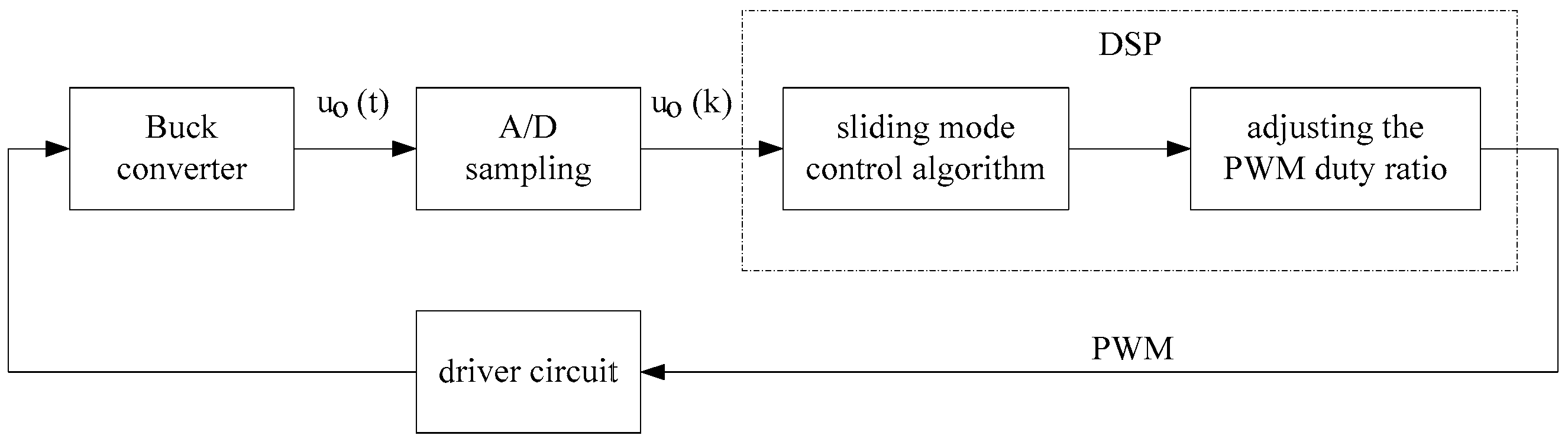
The block diagram of the compound controller for the Buck converter is shown in Figure 2, where the output voltage and inductive current information can be obtained from sensors, and the control output will generate a pulse width modulation (PWM) signal.
4. Simulation Analysis
To verify the feasibility and effectiveness of the proposed algorithm, MATLAB simulations were performed under three kinds of disturbance: start-up, step-load, and step-input-voltage. The converter parameters are given in Table 1.
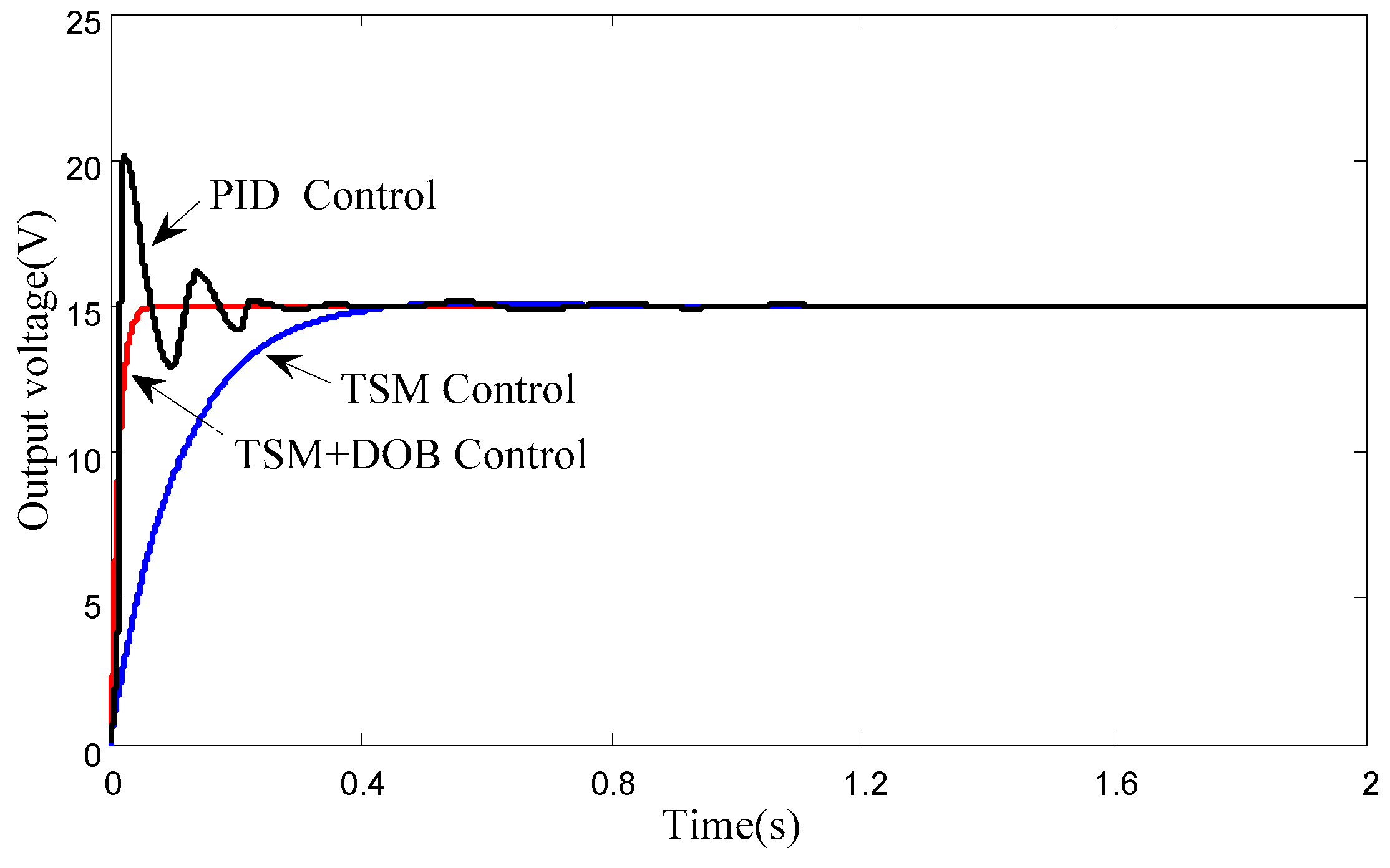
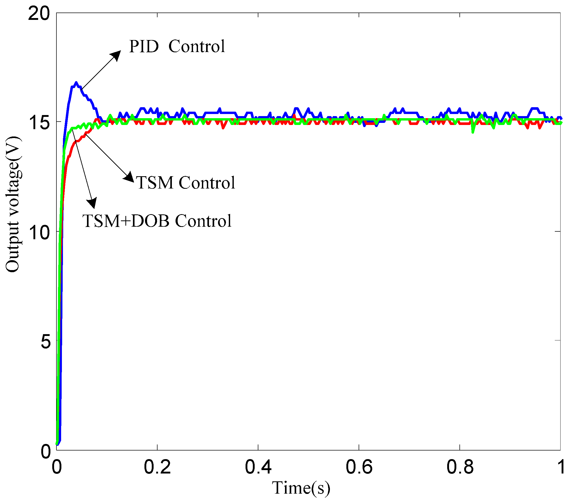
In order to show the advantages of the proposed algorithm, the traditional PID control, terminal sliding mode control (TSM) and compound control (TSM + disturbance observer (DOB)) methods were compared. Firstly, the controller parameters were tuned so that the system under each controller could obtain the best convergence performance. The criterion was to tune the parameters to achieve the fastest convergence without considering the disturbance rejection property. Based on this, the PID parameters were taken as , , and , while the parameters of Controllers (18) and (27) were set as , , and . The boundary layer level was set as and the disturbance observer parameter was chosen to be . For comparison, the simulated start-up waveforms of the traditional PID control, terminal sliding mode (TSM) control, and the compound control (TSM + DOB) methods are shown in Figure 3. The convergence times for the first two cases were both about 0.4 s, while the compound control was found to converge to zero much more quickly—within 0.1 s.
For the disturbance rejection property, the PID controller was always worse than the TSM and compound controllers. This is because the steady-state error under TSM and the compound controllers can be steered to the origin in a finite time, while there always exists a steady-state error under the PID controller. This also implies that no matter what values of parameters are selected, the disturbance rejection properties of the TSM and compound controllers in the simulation will always be better than that of the PID controller.
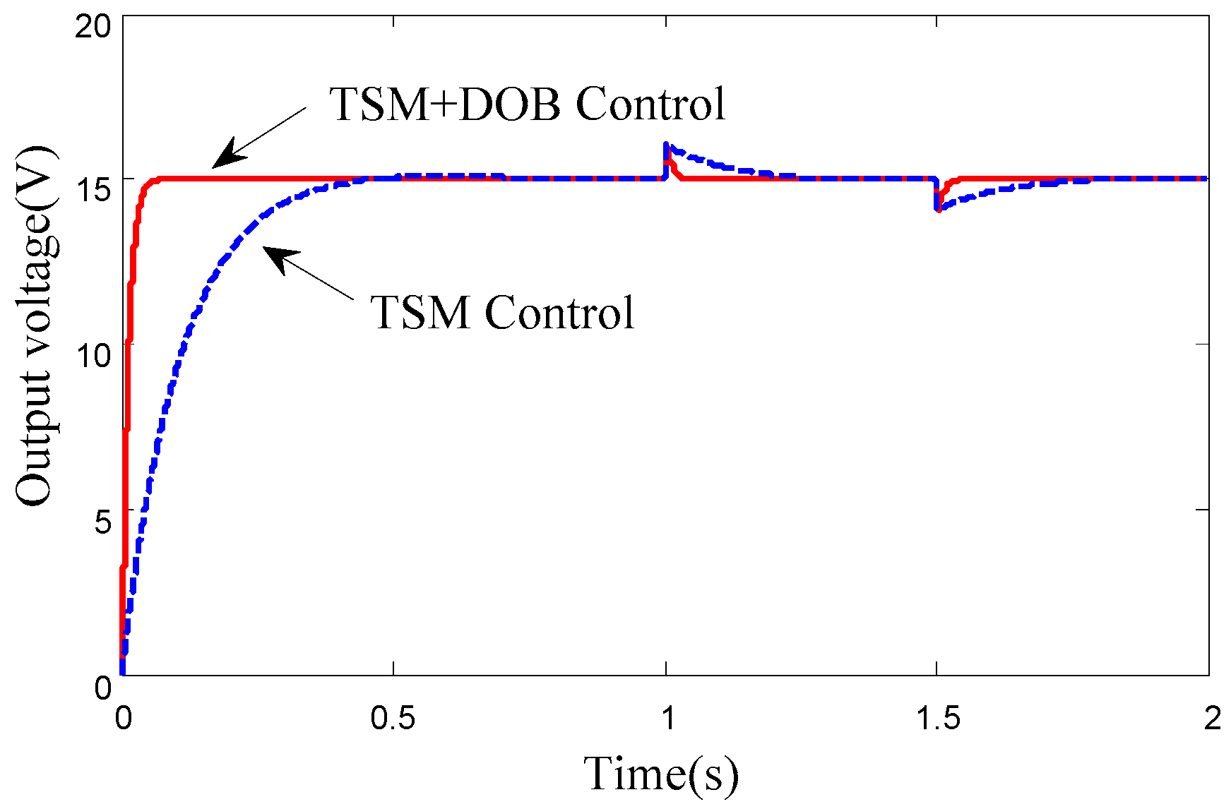
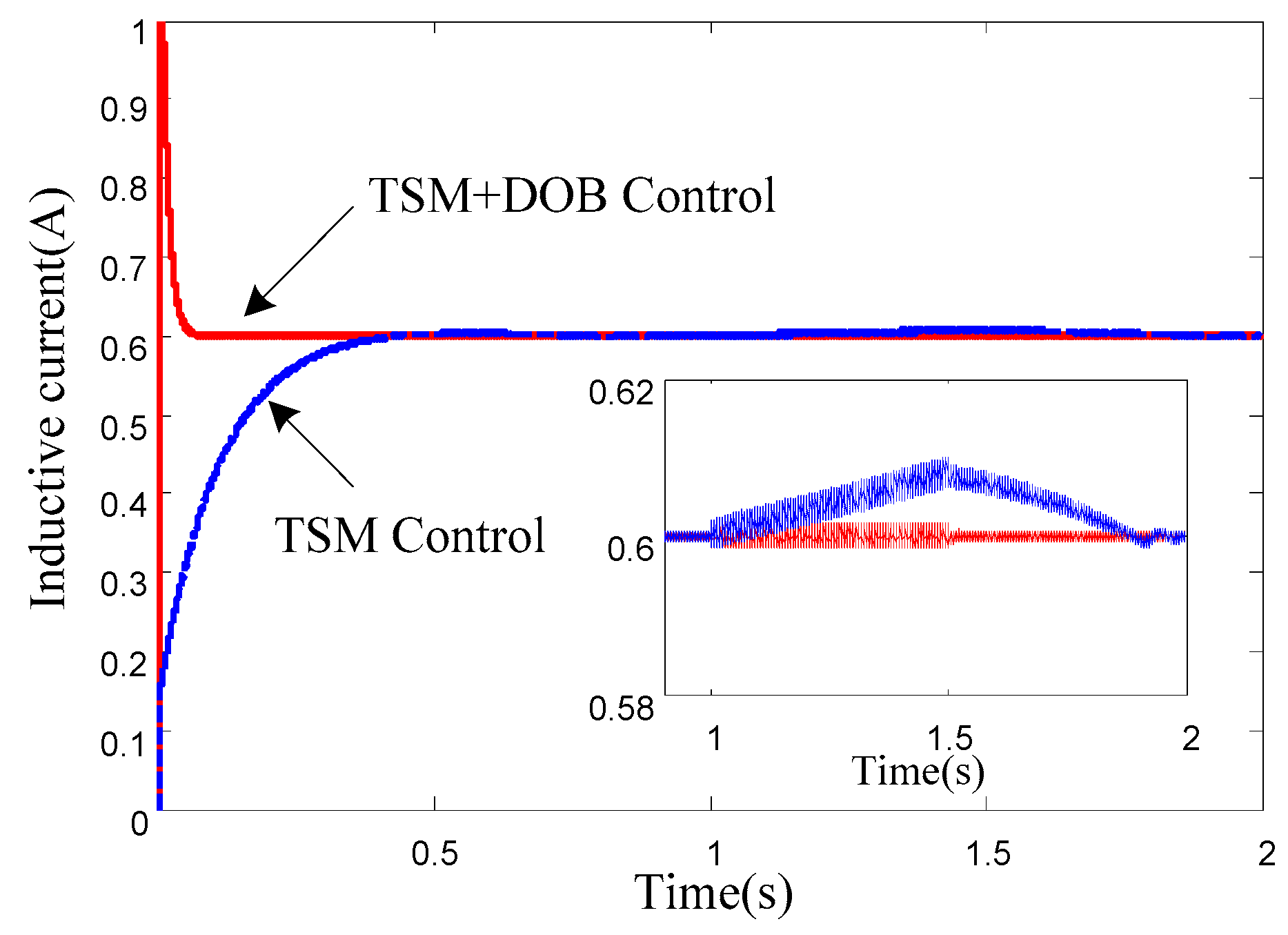
As a matter of fact, from a theoretical point of view, the steady-state error under TSM could be zero in a finite time, while the steady-state error under PID will always be restricted in the region of origin. It is apparent that from the theoretical point of view that the TSM controller could provide a better disturbance rejection property than the PID controller. Hence, we omitted the simulation performed under PID. In Figure 4, the load resistance steps from 25 Ω to 500 Ω at t = 1 s, and back to 25 Ω at t = 1.5 s. The output voltage has a response similar to that of the load resistance. Under the compound controller, it can be observed that the output voltage can return to the steady-state value quickly, and its convergence speed is obviously faster than that of the terminal sliding mode (TSM) controller. The response curves of the inductive current to the step-load are shown in Figure 5. It can also be seen that the current under the compound control can return back to its steady-state value quickly. Therefore, one can conclude that the compound controller with the disturbance observer can provide the system with a faster response speed and better disturbance rejection performance.
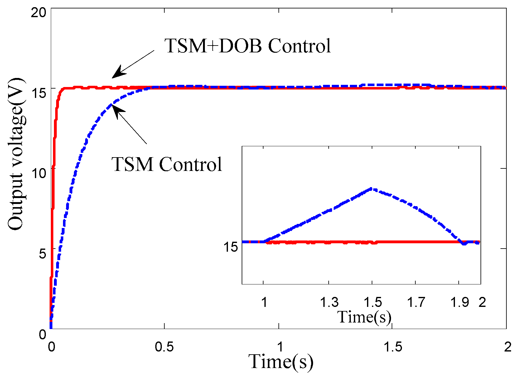
The simulated waveform of the output voltage and inductive current with respect to the input voltage stepping from 30 V to 40 V at t = 1 s and back to 30 V at t = 1.5 s are shown in Figure 6 and Figure 7, respectively. Figure 6 shows that the value of the output voltage increases with the rise of the input voltage. Compared with the traditional terminal sliding mode control, it can be observed that the compound controller with the disturbance observer makes a smaller amplitude change and can quickly converge to the desired value. From Figure 7, we can see that the inductive current under both controllers exhibits a sudden change under TSM and TSM + DOB controllers when the input voltage changes. Nevertheless, the inductive current under the compound controller will reach the steady state rapidly, while the current under the traditional terminal sliding mode controller needs a period of recovery time to reach its steady-state value. In summary, the compound controller has a better control performance.
5. Experimental Verification
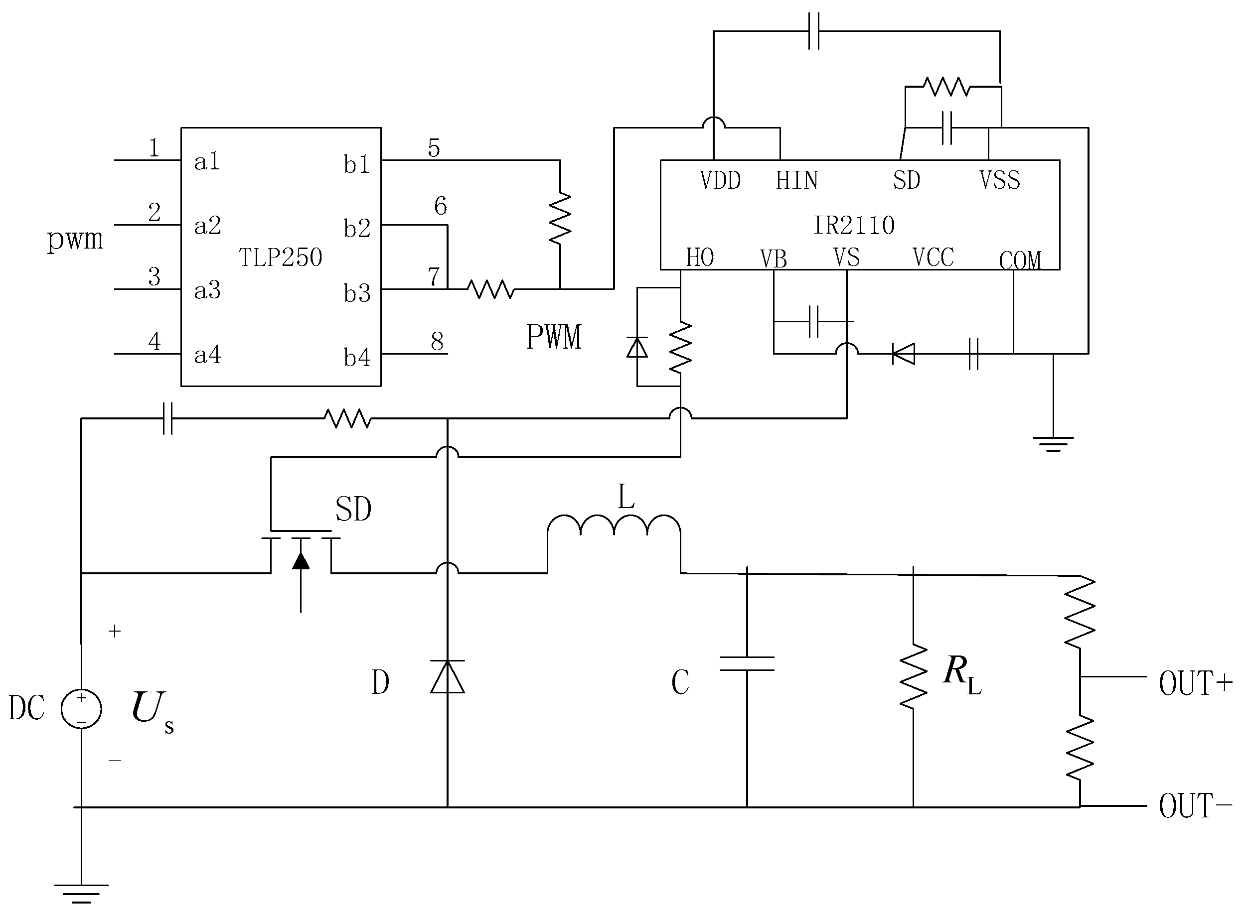
The circuit used in this experiment, shown in Figure 8, was the main circuit of a Buck converter with a 30-V DC voltage as the input. The control algorithms were implemented using digital signal processing (DSP) TMS320F28335 (Texas Instruments Inc., Dallas, TX, USA) with a clock frequency of 150 MHz. The voltage detection adopted the method of parallel resistance, which connects the two series resistors in parallel and adjusts their proportional relationship to meet the voltage sampling range of 0–3.3 V for DSP. The inductive current was measured using the ACS712 current module (Allegro MicroSystems LLC, Worcester, CM, USA). The analog signals of output voltage and inductive current were converted to digital signals through two 12-b analog-to-digital (A/D) converters. The resolution of digital pulse width modulation (DPWM) was 16 bits. The drive circuit adopted TLP250 (Toshiba Inc., Minato-ku, Tokyo, Japan) produced by Toshiba, and the PWM output of DSP was taken as its input signal. Meanwhile the IR2110 chip (International Rectifier Inc., Los Angeles, SC, USA) was bootstrapped, so that the PWM output amplitude was enough to operate the switch. The schematic diagram of the hardware is shown in Figure 8. The TLP250 provided both isolation and driving. In order to stabilize its built-in high-gain amplifier, a small ceramic capacitor and two current-limiting resistors must be placed between b1 and b3. The parameters of the components depend on the operating current of the luminous diode in the chip.
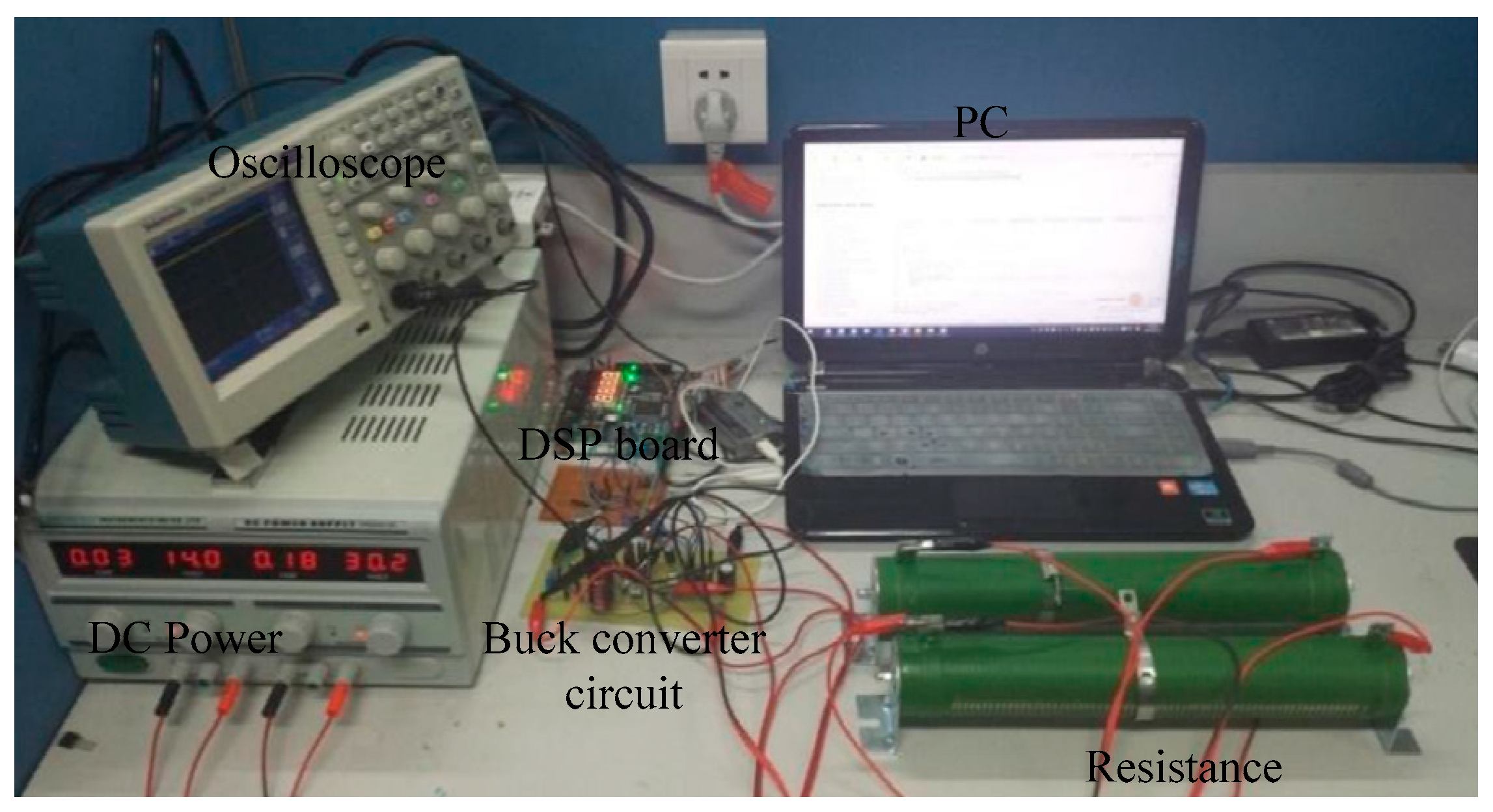
The software of this experiment used DSP as the control chip of the control loop. DSP is widely used in various fields of power electronics because of its fast execution speed, high efficiency, multi-function, and real-time control. The block diagram of the experimental platform is shown in Figure 9. The experimental setup is shown in Figure 10.
The parameters of the electronic elements are: = 330 , = 1000 , = 50 . The TSM coefficients are: , , , while the PID control parameters are: , , .
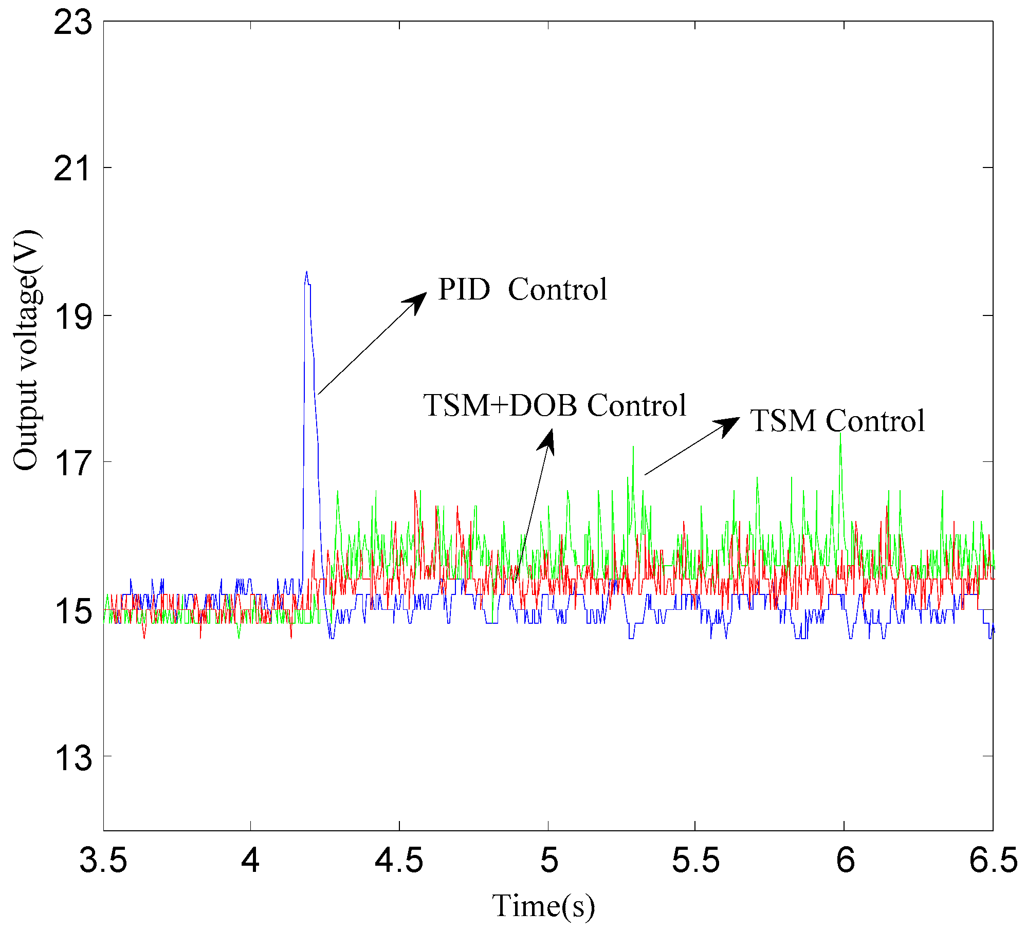
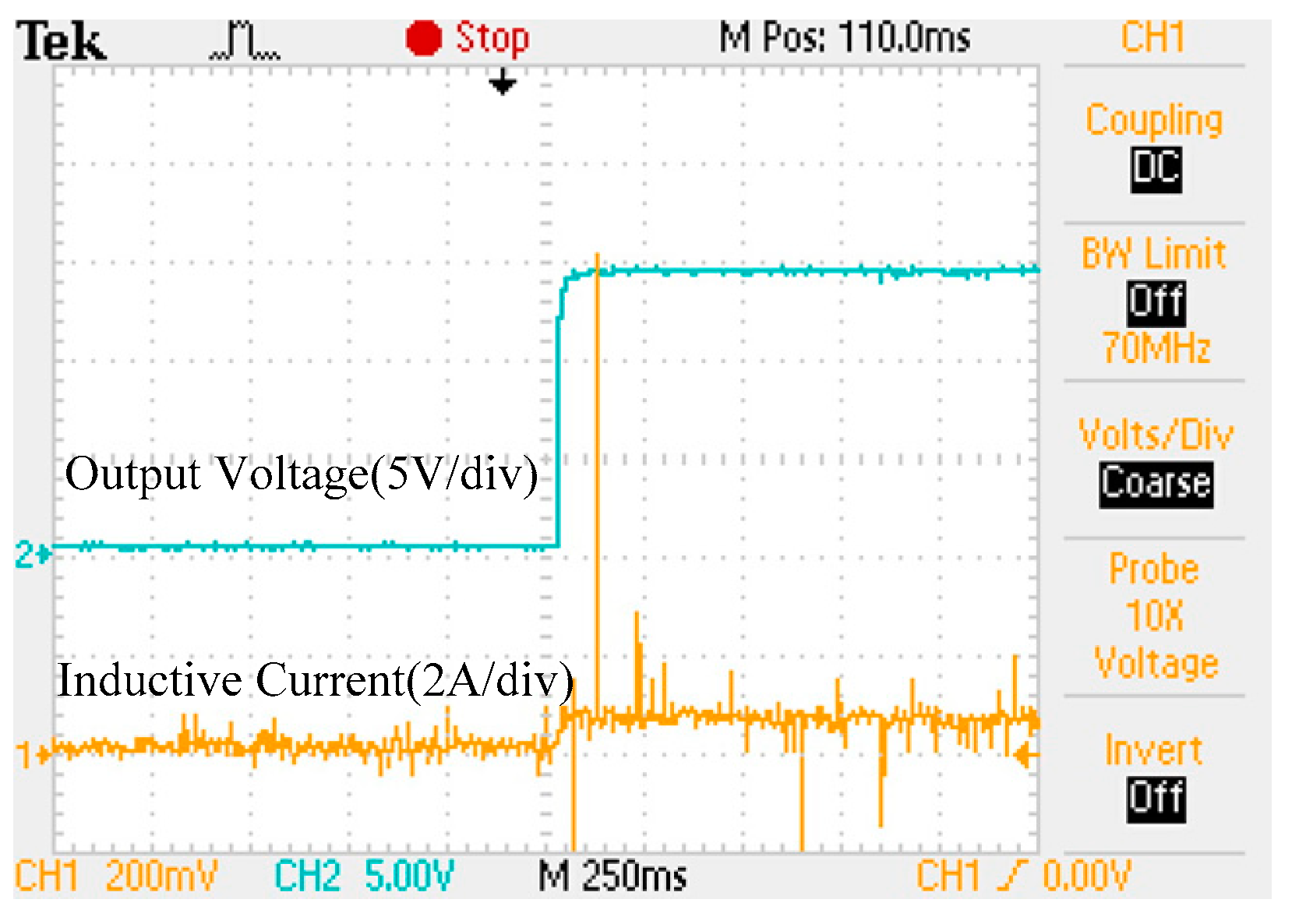
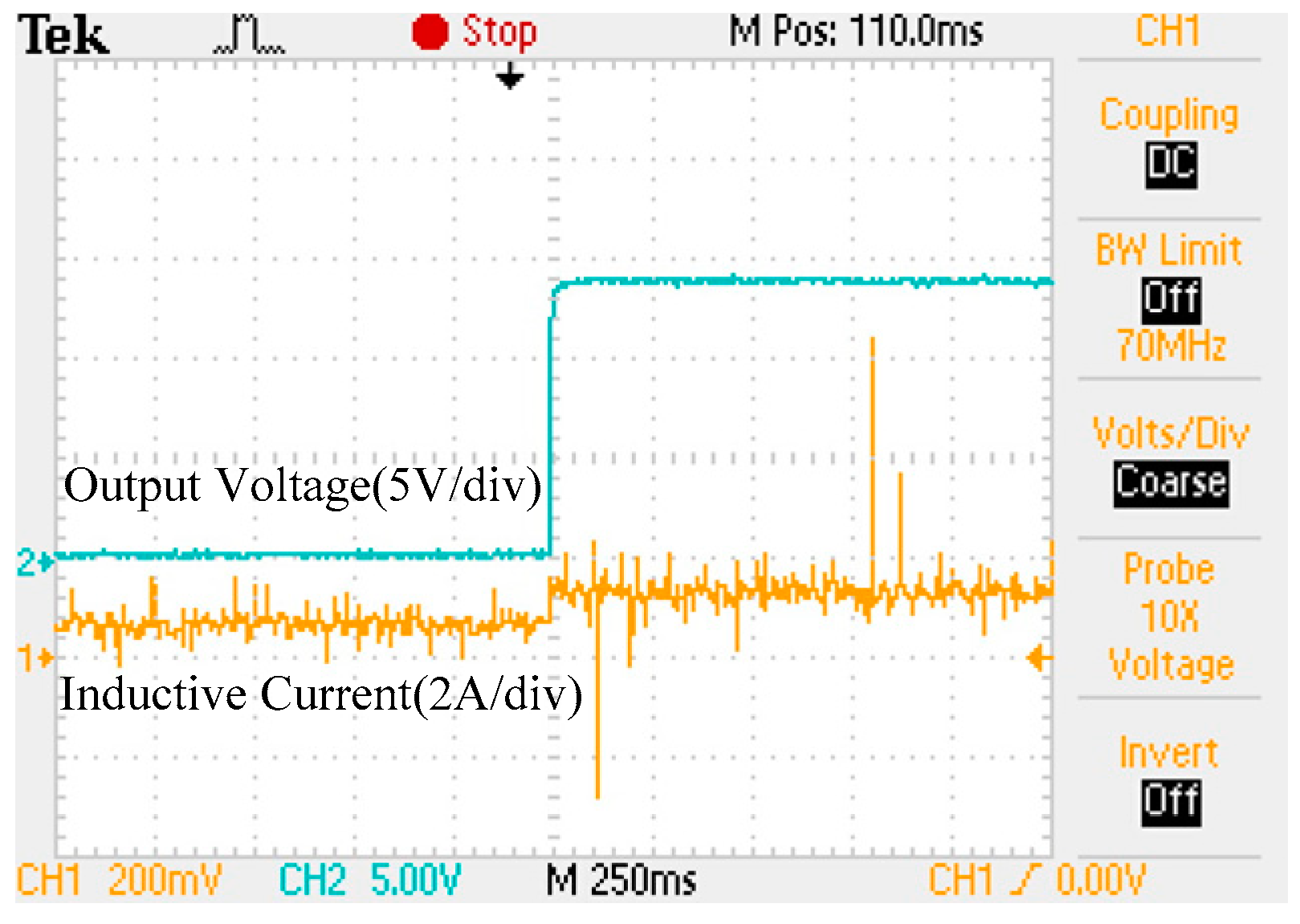
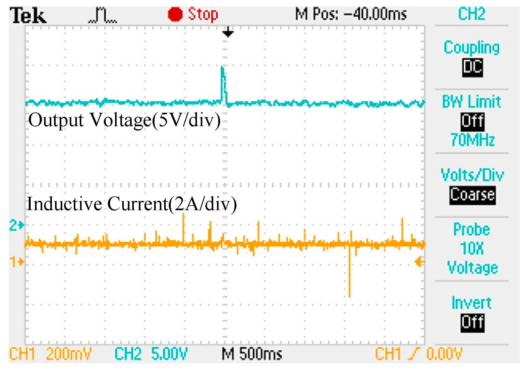
When the input voltage is 30 V and the reference value of the input voltage is 15 V, experimental DC coupled start-up waveforms of the output voltage and inductive current under three control schemes (PID, TSM, TSM + DOB) are shown in Figure 11, Figure 12 and Figure 13. The experimental start-up comparisons of the output voltage are given in Figure 14.
Table 2 gives the comparisons of overshoot, rising time, and settling time under PID, TSM, and TSM + DOB controllers at the start-up. It can be seen that the overshoot under the TSM + DOB controller is smaller than that under the other two control modes. The rising time under the TSM + DOB controller is shorter than that under the other two control modes, with the related rates of 36.4% and 145.5% when comparing with the PID and TSM control modes, respectively. In addition, the settling time under the TSM + DOB controller is also smaller than that under the PID and TSM control modes, with the related rates of 154.5% and 54.5%, respectively.
Experimental DC coupled step-load waveforms of the output voltage and inductive current under three control schemes (PID, TSM, TSM + DOB) when the load steps from 50 to 100 are shown in Figure 15, Figure 16 and Figure 17, and the experimental step-load comparisons of the output voltage are given in Figure 18.
Table 3 gives the comparisons of overshoot and settling time under PID, TSM, and TSM + DOB control modes when the step-load changes. It can be seen that the overshoot under the TSM + DOB controller is smaller than that under the other two control modes. The settling time under the TSM + DOB controller is also shorter than that under the other two control modes, with the related rates of 218.0% and 14.8% when comparing with the PID and TSM control mode, respectively.
Experimental DC coupled step-input-voltage waveforms of the output voltage and inductive current under three control schemes (PID, TSM, TSM + DOB) when the input voltage steps from 30 V to 35 V are shown in Figure 19, Figure 20 and Figure 21, and the experimental step-input-voltage comparisons of the output voltage are given in Figure 22.
Table 4 gives the comparisons of overshoot and settling time under PID, TSM, and TSM + DOB control modes when the step-input-voltage changes. It can be seen that the overshoot under the TSM + DOB controller is smaller than that under the other two control modes. Moreover, the settling time is also shorter than that under the other two control modes, with the related rates of 59.1% and 20.6% when comparing with the PID and TSM control modes, respectively.
From the above experimental results, we can see that in the absence of external disturbances, the terminal sliding mode controller combined with the disturbance observer can quickly reach the desired value, with the overshoot and convergence time being significantly less than those achieved under the other two control schemes. Furthermore, when some disturbances exist, such as the step-load and input-voltage changes, the output voltage of the Buck converter under the compound controller provides the best robustness property. This was confirmed by comparing the overshoot and settling time of the compound controller with those of the other two controllers. The compound controller was found to improve the closed-loop system of Buck converters in two aspects. One is the convergent speed, which implies that the output voltage will converge to the desired voltage rapidly at the start-up. The other is the disturbance rejection property, which provides the control system with strong robustness.
6. Conclusions
In this paper, a new compound control scheme based on terminal sliding mode and nonlinear disturbance observer was proposed for a Buck converter. In comparison to the traditional PID and terminal sliding mode state feedback control modes, this method can provide faster convergence performance and higher voltage output quality for the closed-loop system of a Buck converter. Simulation and experimentation results showed that under the compound control scheme, the system performance of the Buck converter was improved effectively and its robustness was further improved. It can be seen from the experimentations that there always exists a larger steady-state error for the proposed three kinds of controllers. This may be because the power of the Buck converter is lower while the external disturbance is comparatively large. To this end, our future work will focus on DC-DC Buck converters with more power to further test the robustness performances of TSM + DOB algorithms, considering frequency response, dynamic response, immunity to noise, and large-signal stability.
Author Contributions
Conceptualization, L.M.; Methodology and Software, S.D.; Investigation and Writing—Review and Editing, Y.S.; Supervision, D.Z.
Acknowledgments
This work was supported in part by the National Nature Science Foundation of China under Grant 31571571, in part by the Priority Academic Program Development of Jiangsu Higher Education Institutions (PAPD), and in part by the Jiangsu Province Natural Science Fund Project under Grant BK20170536.
Conflicts of Interest
The authors declare no conflict of interest.
References
- Chen, J.J.; Hsu, J.H.; Hwang, Y.S.; Yu, C.C. A DC–DC buck converter with load-regulation improvement using dual-path-feedback techniques. Analog. Integr. Circuits Signal Proc. 2014, 79, 149–159. [Google Scholar] [CrossRef]
- Ding, S.H.; Zheng, W.X.; Sun, J.; Wang, J. Second-order sliding mode controller design and its implementation for buck converters. IEEE Trans. Ind. Inf. 2018, 14, 1990–2000. [Google Scholar] [CrossRef]
- Shabestari, P.M.; Gharehpetian, G.B.; Riahy, G.H.; Mortazavian, S. Voltage controllers for DC-DC boost converters in discontinuous current mode. In Proceedings of the International Energy and Sustainability conference (IESC), New York, NY, USA, 12–13 November 2015; pp. 1–7. [Google Scholar]
- Kancherla, S.; Tripathi, R.K. Nonlinear average current mode control for a DC-DC Buck converter. In Proceedings of the IEEE International Conference on Sustainable Energy Technologies, Singapore, 24–27 November 2008; pp. 831–836. [Google Scholar]
- Tan, S.C.; Lai, Y.M.; Cheung, M.K.H.; Tse, C.K. On the practical design of a sliding mode voltage controlled buck converter. IEEE Trans. Power Electron. 2005, 20, 425–437. [Google Scholar] [CrossRef] [Green Version]
- Zhang, Y.; Zhang, B.; Chen, B.; Hu, Z. A Novel Control Law of Boost DC-DC Converter Based on Bilinear Theory. Trans. China Electrotech. Soc. 2006, 21, 109–114. [Google Scholar]
- Tan, S.C.; Lai, Y.M.; Chi, K.T. General Design Issues of Sliding-Mode Controllers in DC-DC Converters. IEEE Trans. Ind. Electron. 2008, 55, 1160–1174. [Google Scholar]
- Ni, Y.; Xu, J.P. Design of a novel discrete global sliding mode controlled Buck converter. Electr. Mach. Control 2009, 23, 112–116. [Google Scholar]
- Komurcugil, H. Non-singular terminal sliding-mode control of DC-DC buck converters. Control Eng. Pract. 2013, 21, 321–332. [Google Scholar] [CrossRef]
- Delgado, F.; Magana, M.E. A fuzzy logic controller design and simulation for a sawmill bucking system. IEEE Trans. Ind. Electron. 2005, 52, 628–634. [Google Scholar] [CrossRef]
- Alrabadi, A.N.; Barghash, M.A.; Abuzeid, O.M. Intelligent Regulation Using Genetic Algorithm-Based Tuning for the Fuzzy Control of the Power Electronic Switching-Mode Buck Converter. Available online: https://pdfs.semanticscholar.org/ea48/74ac9caac6bfccaa70c3b767f54d6eb52a41.pdf (accessed on 12 February 2018).
- Saravanan, A.G.; Rajaram, M. Fuzzy controller for dynamic performance improvement of a half-bridge isolated dc–dc converter. Neurocomputing 2014, 140, 283–290. [Google Scholar] [CrossRef]
- Piazza, M.C.D.; Pucci, M.; Ragusa, A.; Vitale, G. Analytical versus neural real-time simulation of a photovoltaic generator based on a DC-DC converter. IEEE Trans. Ind. Appl. 2010, 46, 2501–2510. [Google Scholar] [CrossRef]
- Bïngöl, O.; Pacaci, S. A Virtual Laboratory for Neural Network Controlled DC Motors Based on a DC-DC Buck Converter. Int. J. Eng. Educ. 2012, 28, 713–723. [Google Scholar]
- Salimi, M.; Soltani, J.; Markadeh, G.A.; Abjadi, N.R. Adaptive nonlinear control of the DC-DC buck converters operating in CCM and DCM. Eur. Trans. Electr. Power 2012, 23, 1536–1547. [Google Scholar] [CrossRef]
- Babazadeh, A.; Maksimovic, D. Hybrid Digital Adaptive Control for Fast Transient Response in Synchronous Buck DC–DC Converters. IEEE Trans. Power Electron. 2009, 24, 2625–2638. [Google Scholar] [CrossRef]
- Vatankhah, B.; Farrokhi, M. Offset-free adaptive nonlinear model predictive control with disturbance observer for dc-dc buck converters. Turk. J. Electr. Eng. Comput. Sci. 2017, 25, 2195–2206. [Google Scholar] [CrossRef]
- Ding, S.H.; Wang, J.D.; Zheng, W.X. Second-order sliding mode control for nonlinear uncertain systems bounded by positive functions. IEEE Trans. Ind. Electron. 2015, 62, 5899–5909. [Google Scholar] [CrossRef]
- Ding, S.H.; Liu, L.; Zheng, W.X. Sliding mode direct yaw-moment control design for in-wheel electric vehicles. IEEE Trans. Ind. Electron. 2017, 64, 6752–6762. [Google Scholar] [CrossRef]
- Xie, X.Z. Observer-based nonsingular terminal sliding mode controller design. In Proceedings of the 24th Chinese Control and Decision Conference (CCDC), Taiyuan, China, 23–25 May 2012; pp. 454–458. [Google Scholar]
- Qi, W.H.; Zong, G.D.; Karim, H.R. Observer-based adaptive SMC for nonlinear uncertain singular semi-Markov jump systems with applications to DC motor. IEEE Trans. Circuit. Syst. I Regul. Pap. 2018, 65, 2951–2960. [Google Scholar] [CrossRef]
- Ni, Y.; Xu, J.P.; Wang, J.P.; Yu, H.K. Design of global sliding mode control Buck converter with hysteresis modulation. Proc. Chin. Soc. Electr. Eng. 2010, 30, 1–6. [Google Scholar]
- Naik, B.B.; Mehta, A.J. Sliding mode controller with modified sliding function for DC-DC Buck Converter. ISA Trans. 2017, 70, 1–5. [Google Scholar] [CrossRef] [PubMed]
- Komurcugil, H. Adaptive terminal sliding-mode control strategy for DC-DC buck converters. ISA Trans. 2012, 51, 673–681. [Google Scholar] [CrossRef] [PubMed]
- Wang, J.X.; Li, S.H.; Yang, J.; Wu, B.; Li, Q. Finite-time disturbance observer based non-singular terminal sliding-mode control for pulse width modulation based dc–dc buck converters with mismatched load disturbances. IET Power Electron. 2016, 9, 1995–2002. [Google Scholar] [CrossRef]
- Zhao, Z.; Yang, J.; Li, S.; Yu, X.; Wang, Z. Continuous output feedback TSM control for uncertain systems with a DC-AC inverter example. IEEE Trans. Circuit. Syst. II Express Br. 2018, 65, 71–75. [Google Scholar] [CrossRef]
- Zhang, C.L.; Wang, J.X.; Li, S.H.; Wu, B.; Qian, C.J. Robust control for PWM-based DC–DC buck power converters with uncertainty via sampled-data output feedback. IEEE Trans. Power Electron. 2015, 30, 504–515. [Google Scholar] [CrossRef]
- Yang, J.; Ding, Z. Global output regulation for a class of lower triangular nonlinear systems: A feedback domination approach. Automatica 2017, 76, 65–69. [Google Scholar] [CrossRef] [Green Version]
- Ding, S.H.; Li, S.H. Second-order sliding mode controller design subject to mismatched term. Automatica 2017, 77, 388–392. [Google Scholar] [CrossRef]
- Du, H.B.; Yu, X.H.; Chen, M.Z.Q.; Li, S.H. Chattering-free discrete-time sliding mode control. Automatica 2016, 68, 87–91. [Google Scholar] [CrossRef]
- Wang, J.; Liang, K.; Huang, X.; Wang, Z.; Shen, H. Dissipative fault-tolerant control for nonlinear singular perturbed systems with markov jumping parameters based on slow state feedback. Appl. Math. Comput. 2018, 328, 247–262. [Google Scholar] [CrossRef]
- Shen, H.; Li, F.; Xu, S.; Sreeram, V. Slow state variables feedback stabilization for semi-markov jump systems with singular perturbations. IEEE Trans. Autom. Control 2017, 63, 2709–2714. [Google Scholar] [CrossRef]
- Cheng, J.; Chang, X.H.; Ju, H.P.; Li, H.; Wang, H. Fuzzy-model-based H∞ control for discrete-time switched systems with quantized feedback and unreliable links. Inf. Sci. 2018, 436–437, 181–196. [Google Scholar] [CrossRef]
- Bhat, S.P. Finite-time stability of continuous autonomous systems. SIAM J. Control Optim. 2000, 38, 751–766. [Google Scholar] [CrossRef]
- Cheng, J.; Ju, H.P.; Karimi, H.R.; Hao, S. A flexible terminal approach to sampled-data exponentially synchronization of Markovian neural networks with time-varying delayed signals. IEEE Trans. Cybern. 2018, 48, 2232–2244. [Google Scholar] [PubMed]
- Ge, C.; Wang, B.; Wei, X.; Liu, Y. Exponential synchronization of a class of neural networks with sampled-data control. Appl. Math. Comput. 2017, 315, 150–161. [Google Scholar] [CrossRef]
- Zhang, C.L.; Yan, Y.D.; Narayan, A.; Yu, H.Y. Practically oriented finite-time control design and implementation: Application to series elastic actuator. IEEE Trans. Ind. Electron. 2018, 65, 4166–4176. [Google Scholar] [CrossRef]
- Li, S.H.; Yang, J.; Chen, W.H.; Chen, X. Disturbance Observer Based Control: Methods and Applications; CRC Press: Boca Raton, FL, USA, 2014. [Google Scholar]
Figure 1.
Circuit diagram of the Buck converter.
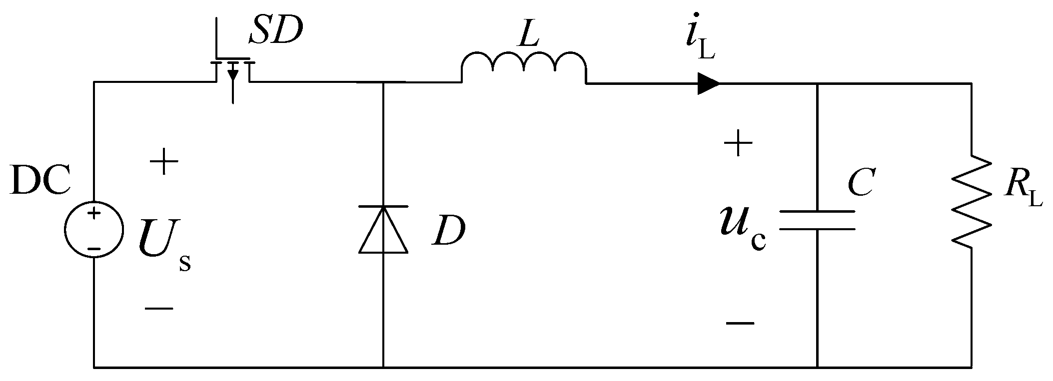
Figure 2.
Block diagram of the compound controller for the Buck converter.

Figure 3.
Simulated start-up waveform of output voltage in the absence of disturbance.

Figure 4.
Simulated step-load waveform of the output voltage.

Figure 5.
Simulated step-load waveform of the inductive current.
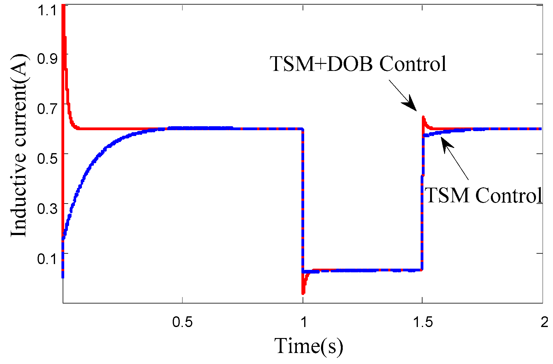
Figure 6.
Simulated step-input-voltage waveform of the output voltage.

Figure 7.
Simulated step-input-voltage waveform of the inductive current.

Figure 8.
The schematic diagram of the hardware.

Figure 9.
The block diagram of the experimental platform.

Figure 10.
Experimental setup.

Figure 11.
Experimental start-up waveforms of the output voltage and inductive current under the proportional integral derivative (PID) controller.
Figure 11.
Experimental start-up waveforms of the output voltage and inductive current under the proportional integral derivative (PID) controller.
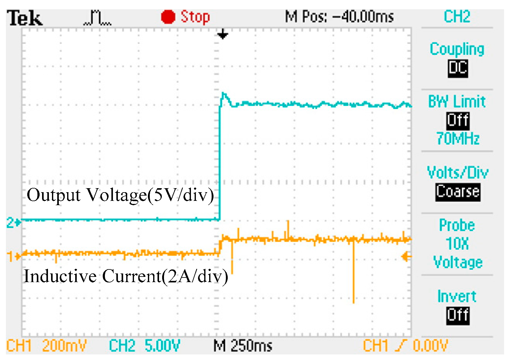
Figure 12.
Experimental start-up waveforms of the output voltage and inductive current under the terminal sliding mode (TSM) controller.
Figure 12.
Experimental start-up waveforms of the output voltage and inductive current under the terminal sliding mode (TSM) controller.

Figure 13.
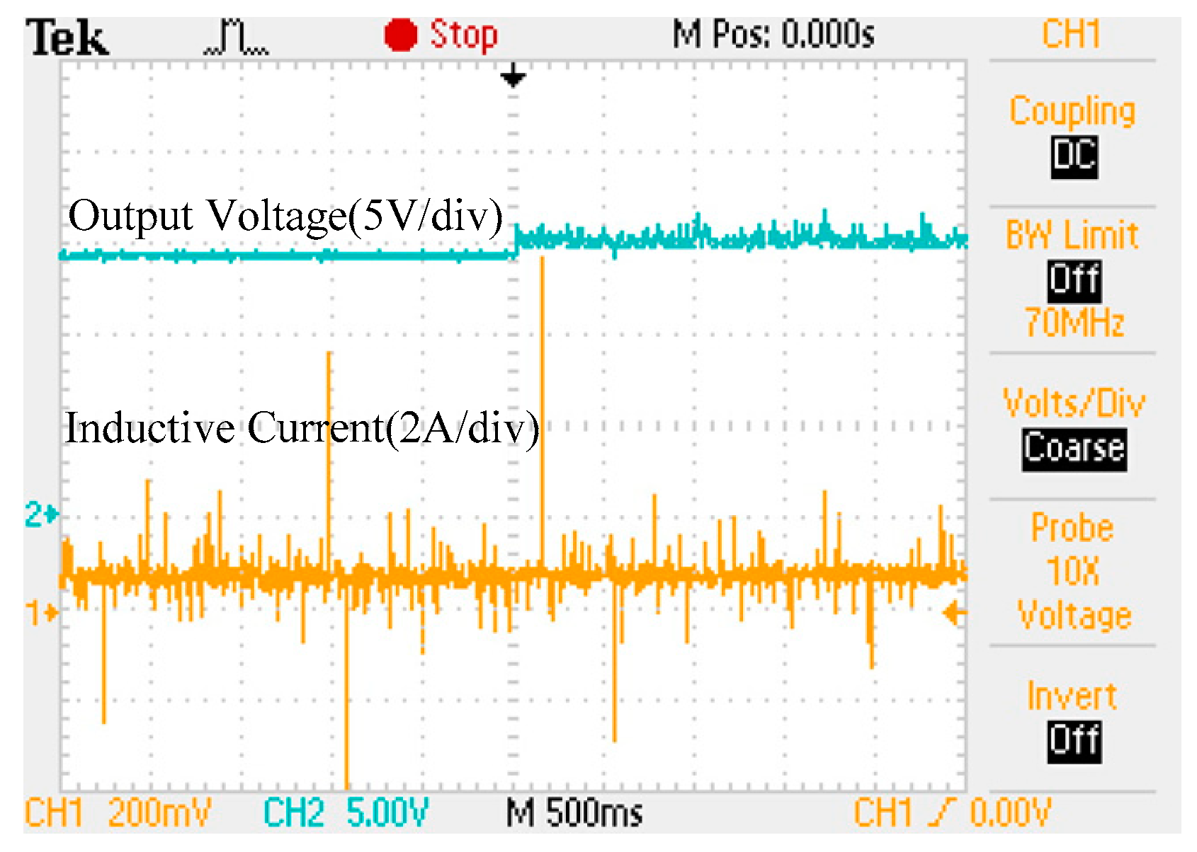
Experimental start-up waveforms of the output voltage and inductive current under the TSM + disturbance observer (DOB) controller.
Figure 13.
Experimental start-up waveforms of the output voltage and inductive current under the TSM + disturbance observer (DOB) controller.

Figure 14.
Experimental start-up comparisons of the output voltage under PID, TSM, and TSM + DOB controllers.
Figure 14.
Experimental start-up comparisons of the output voltage under PID, TSM, and TSM + DOB controllers.

Figure 15.
Experimental step-load waveforms of the output voltage and inductive current under the PID controller.
Figure 15.
Experimental step-load waveforms of the output voltage and inductive current under the PID controller.
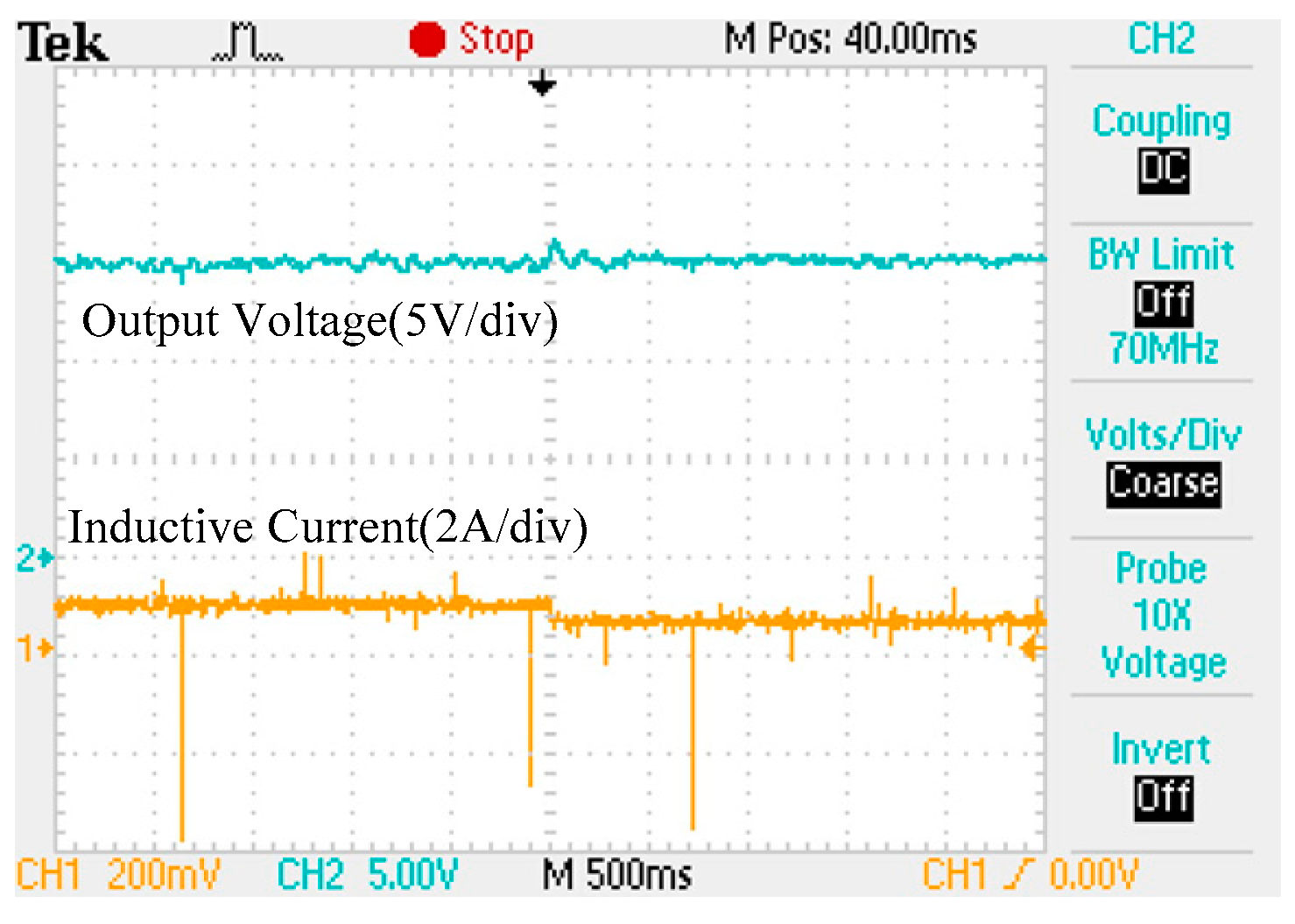
Figure 16.
Experimental step-load waveforms of the output voltage and inductive current under the TSM controller.
Figure 16.
Experimental step-load waveforms of the output voltage and inductive current under the TSM controller.
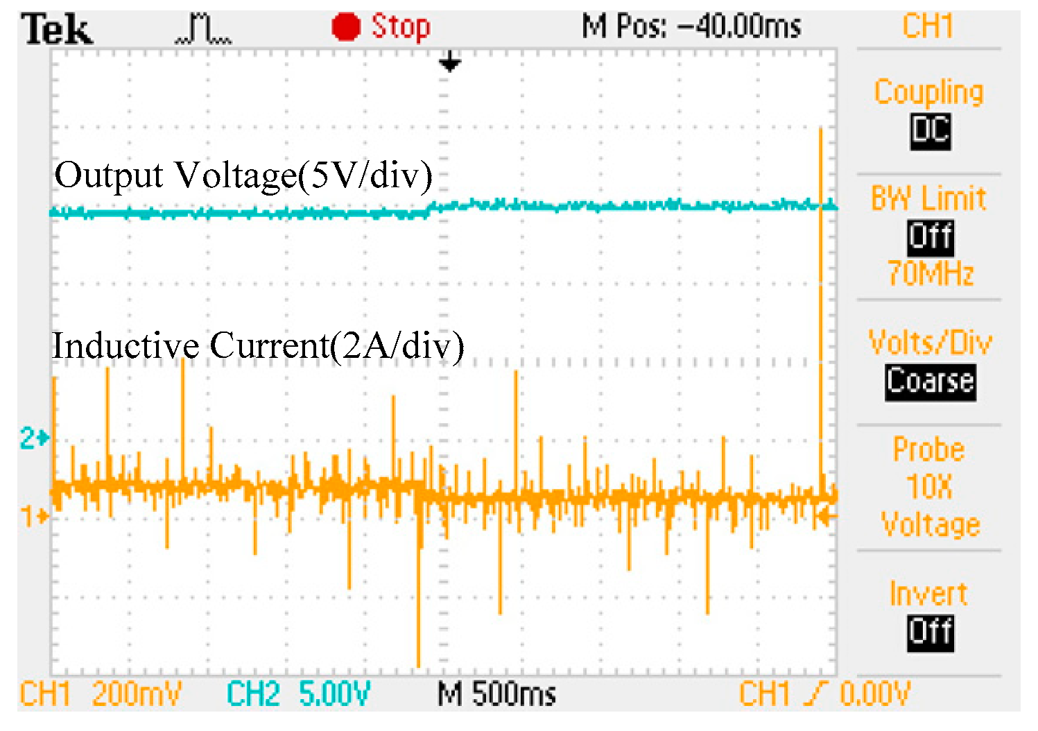
Figure 17.
Experimental step-load waveforms of the output voltage and inductive current under the TSM + DOB controller.
Figure 17.
Experimental step-load waveforms of the output voltage and inductive current under the TSM + DOB controller.
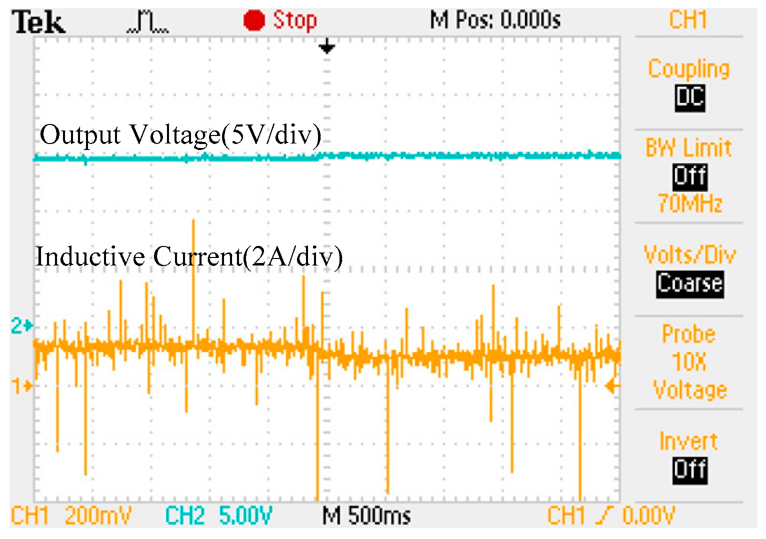
Figure 18.
Experimental step-load comparisons of the output voltage under PID, TSM, and TSM + DOB control modes.
Figure 18.
Experimental step-load comparisons of the output voltage under PID, TSM, and TSM + DOB control modes.
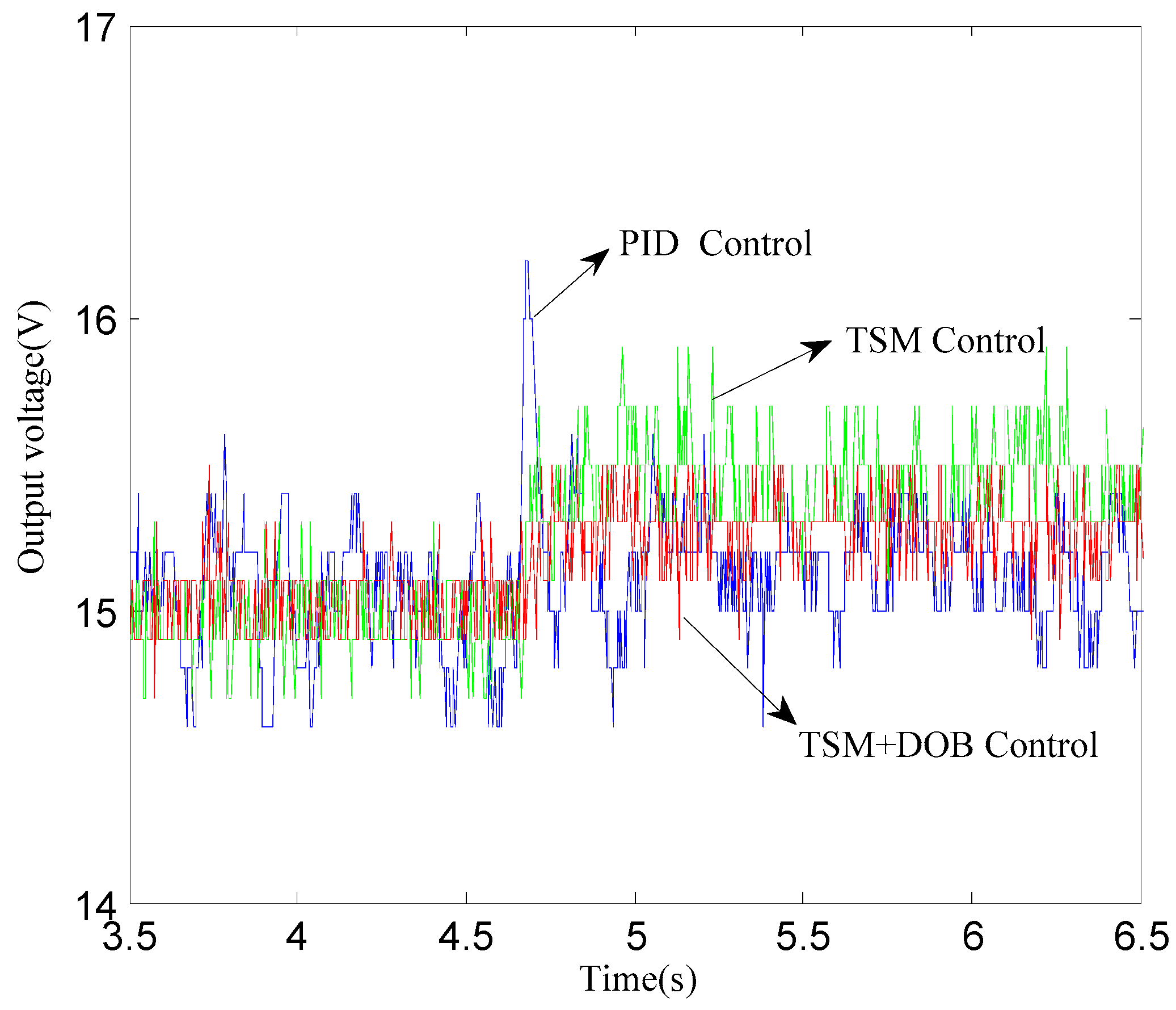
Figure 19.
Experimental step-input-voltage waveforms of the output voltage and inductive current under the PID controller.
Figure 19.
Experimental step-input-voltage waveforms of the output voltage and inductive current under the PID controller.

Figure 20.
Experimental step-input-voltage waveforms of the output voltage and inductive current under the TSM controller.
Figure 20.
Experimental step-input-voltage waveforms of the output voltage and inductive current under the TSM controller.

Figure 21.
Experimental step-input-voltage waveforms of the output voltage and inductive current under the TSM + DOB controller.
Figure 21.
Experimental step-input-voltage waveforms of the output voltage and inductive current under the TSM + DOB controller.
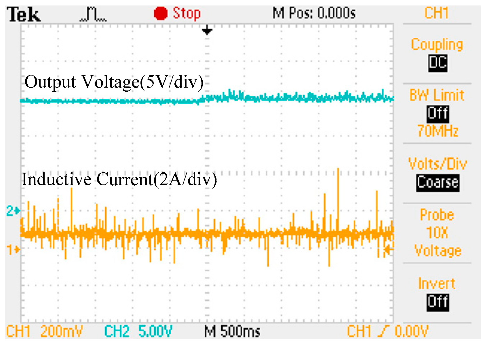
Figure 22.
Experimental step-input-voltage comparisons of the output voltage under PID, TSM, and TSM + DOB control modes.
Figure 22.
Experimental step-input-voltage comparisons of the output voltage under PID, TSM, and TSM + DOB control modes.

Table 1.
Parameters of the converter.
| Parameter | Value |
|---|---|
| Input voltage, Us | 30 V |
| Inductance, L | 330 μH |
| Capacitance, C | 1000 pF |
| Load resistance, RL | 25 Ω |
| Voltage reference, V0 | 15 V |
Table 2.
Comparisons under proportional integral derivative (PID), terminal sliding mode control (TSM), and TSM + disturbance observer (DOB) at the start-up.
Table 2.
Comparisons under proportional integral derivative (PID), terminal sliding mode control (TSM), and TSM + disturbance observer (DOB) at the start-up.
| Controller | Overshoot (V) | Rising Time (ms) | Settling Time (ms) |
|---|---|---|---|
| PID | 1.8 | 41.7 | 388.9 |
| TSM | 0.4 | 75.0 | 236.1 |
| TSM + DOB | 0.3 | 30.6 | 152.8 |
Table 3.
Comparisons under PID, TSM, and TSM + DOB when the step-load changes.
| Controller | Overshoot (V) | Settling Time (ms) |
|---|---|---|
| PID | 1.2 | 294.5 |
| TSM | 0.6 | 106.3 |
| TSM + DOB | 0.4 | 92.6 |
Table 4.
Comparisons under PID, TSM, and TSM + DOB when the step-input-voltage changes.
| Controller | Overshoot (V) | Settling Time (ms) |
|---|---|---|
| PID | 4.6 | 112.6 |
| TSM | 1.2 | 85.4 |
| TSM + DOB | 1.0 | 70.8 |
© 2018 by the authors. Licensee MDPI, Basel, Switzerland. This article is an open access article distributed under the terms and conditions of the Creative Commons Attribution (CC BY) license (http://creativecommons.org/licenses/by/4.0/).
Share and Cite
MDPI and ACS Style
Sun, Y.; Ma, L.; Zhao, D.; Ding, S. A Compound Controller Design for a Buck Converter. Energies 2018, 11, 2354. https://doi.org/10.3390/en11092354
AMA Style
Sun Y, Ma L, Zhao D, Ding S. A Compound Controller Design for a Buck Converter. Energies. 2018; 11(9):2354. https://doi.org/10.3390/en11092354
Chicago/Turabian StyleSun, Yueping, Li Ma, Dean Zhao, and Shihong Ding. 2018. "A Compound Controller Design for a Buck Converter" Energies 11, no. 9: 2354. https://doi.org/10.3390/en11092354
Note that from the first issue of 2016, this journal uses article numbers instead of page numbers. See further details here.