A 120 W Class-E Power Module with an Adaptive Power Combiner for a 6.78 MHz Wireless Power Transfer System


Department of Electronic Engineering, Yeungnam University, 280 Daehak-ro, Gyeongsan 38541, Gyeongbuk, Korea
*
Author to whom correspondence should be addressed.
Energies 2018, 11(8), 2083; https://doi.org/10.3390/en11082083
Submission received: 30 June 2018
/
Revised: 30 July 2018
/
Accepted: 7 August 2018
/
Published: 10 August 2018
Abstract
:In this article, a highly efficient power module is presented with two class-E power amplifiers and an adaptive power combiner for transmitting output powers >100 W at 6.78 MHz in a wireless power transfer system. The losses caused by the combiners and interstage matching circuits or mismatching between the amplifier, and the combiners can significantly reduce the overall efficiency of the power module. To achieve an efficient combination of the output amplifier signals, the adaptive power combiner is proposed based on the consideration of the optimum load impedance characteristics of the power amplifiers. The input impedance of the combiner is designed using series capacitors and resistors between the two input ports of the combiner and the two output signals of the class-E amplifiers at the optimum load condition. The output performances of the proposed module can decrease based on the component mismatch between the two power amplifiers. The proposed power module was implemented on an FR4 PCB, with a 15 mm metal heat sink, and demonstrated an output power of 123.3 W, a power-added efficiency of 85.7%, and a power gain of 25.6 dB at 6.78 MHz. The second harmonic suppression of the module was 37 dBc.
1. Introduction
After the demonstration of the wireless power transfer technology, originally proposed by N. Tesla, as a wireless power transmission at a distance of 2 m at the Massachusetts Institute of Technology (MIT), this system has been applied to a variety of consumer applications [1,2,3]. Conventional application systems have been used for wireless charging of tablets and cell phones that require a power of, at most, 15 W [4,5]. Recently, the specification of the system that is capable of supplying more than 60 W of power to target devices has also been discussed in the Wireless Power Consortium (WPC) to expand the range of applications in consumer electronics and other devices, such as laptops, power tools, household appliances, medical devices and equipment, and electric bicycles [6,7,8]. The delivered power to the load can be described as the multiplication of the coupling efficiency between the transmitter and receiver, alternating current (AC)-to-direct current (DC) conversion efficiency at the receiver, and the transmitted power at the highly efficient transmitter [9]. An output transmitted power of over 100 W is required to obtain a delivered power of over 60 W, when the coupling and the power conversion efficiencies are assumed to be 70% and 90%, respectively. It is also necessary to transmit enough power (more than 100 W) at the transmitter with operation stability because the coupling efficiency decreases as the distance between the transmitter and the receiver increases.
The transmitting efficiency of the high-power transmitter is one of the most important specifications in the wireless power transfer system because low efficiency in the power transmitting module increases the heat generation at the transmitter, which can lower the operating stability and noise signals in the air, ultimately causing possible interference with other wireless systems [10]. The power module generally consists of the signal generator, which generates the wireless signals, and the power amplifier (PA) which amplifies the output power. Correspondingly, the efficiency of the module can be represented by the power-added efficiency (PAE) of the PA because most of the DC power is consumed at the amplifier. The highly efficient PA design, with an output power exceeding 100 W, is a mandatory factor in determining whether a wireless charging or power transmission system can be implemented or not for a specific/targeted application.
The loosely coupled wireless power transfer system at 6.78 MHz, which uses the self-resonance effect that occurs between adjacent coils, has advantages in wireless power transmission to a plurality of terminals. Therefore, it is not necessary to accurately align the transmitter and the receiver [11,12]. A class-E PA, which can amplify 6.78 MHz signals with a high efficiency using a single switching transistor, is a useful circuit for the power module in the loosely coupled wireless power transfer system because of the simple configuration and easy design [13]. However, it is difficult to increase the PAE of the 100 W class-E PA using a single switching transistor at 6.78 MHz because the transistor should have the characteristics of a low on-resistance and a high-breakdown voltage at the operating frequency. The excess heat generated in the module with over 100 W output power also affects the characteristics of the switching transistor of the PA, and it causes the efficiency of the power module to be lowered even more. The distributed PAs with power combiners can be used to prevent performance degradation due to the generated heat [14], but the loss caused by the combiners and interstage matching circuits, or mismatching between the PA and the combiners, may also significantly reduce the overall efficiency of the power module [15].
In this paper, the class-E power module is proposed with an output power exceeding 120 W as a highly efficient transmitter for the 6.78 MHz wireless power transfer system. The proposed module consists of two highly efficient PAs using laterally diffused metal oxide semiconductor (LDMOS) switching transistors and an adaptive power combiner operating simultaneously as an impedance transformer and a power combiner. The class-E amplifier is designed at 6.78 MHz, with an optimal output impedance to achieve the maximum PAE and an output power in excess of 50 W. The 6.78 MHz signal, that is amplified with a high efficiency at the optimum impedance, is transmitted to the input port of the proposed combiner, and the output signal is obtained at the load of the power module, with a total power in excess of 100 W, given a reference impedance of 50 Ω. The proposed module, including the PAs and combiner, was designed on an FR4 printed circuit board (PCB) using an electromagnetic (EM) field and a radio frequency (RF) circuit co-simulation process. Simulation results demonstrated that the proposed power module increased both the PAE and the maximum output power compared to a single class-E PA using the same switching transistor [16]. Based on the variation of the overall PAE due to the impedance mismatch between the PAs and the combiner, and the effect caused by the characteristic difference of two PAs, the stability and operation characteristics of the module are analyzed using the measurement results. Section 2 describes the schematic design and characteristics of the class-E PA and the proposed power module, including the EM field and RF circuit co-simulation. The implementation and the measured results of the module are detailed in Section 3. The analyses on the characteristics of the module are discussed in Section 4. Conclusions are presented in Section 5.
2. Design of the Class-E Power Module
2.1. Class-E Power Amplifiers Using an L-Type Matching Network
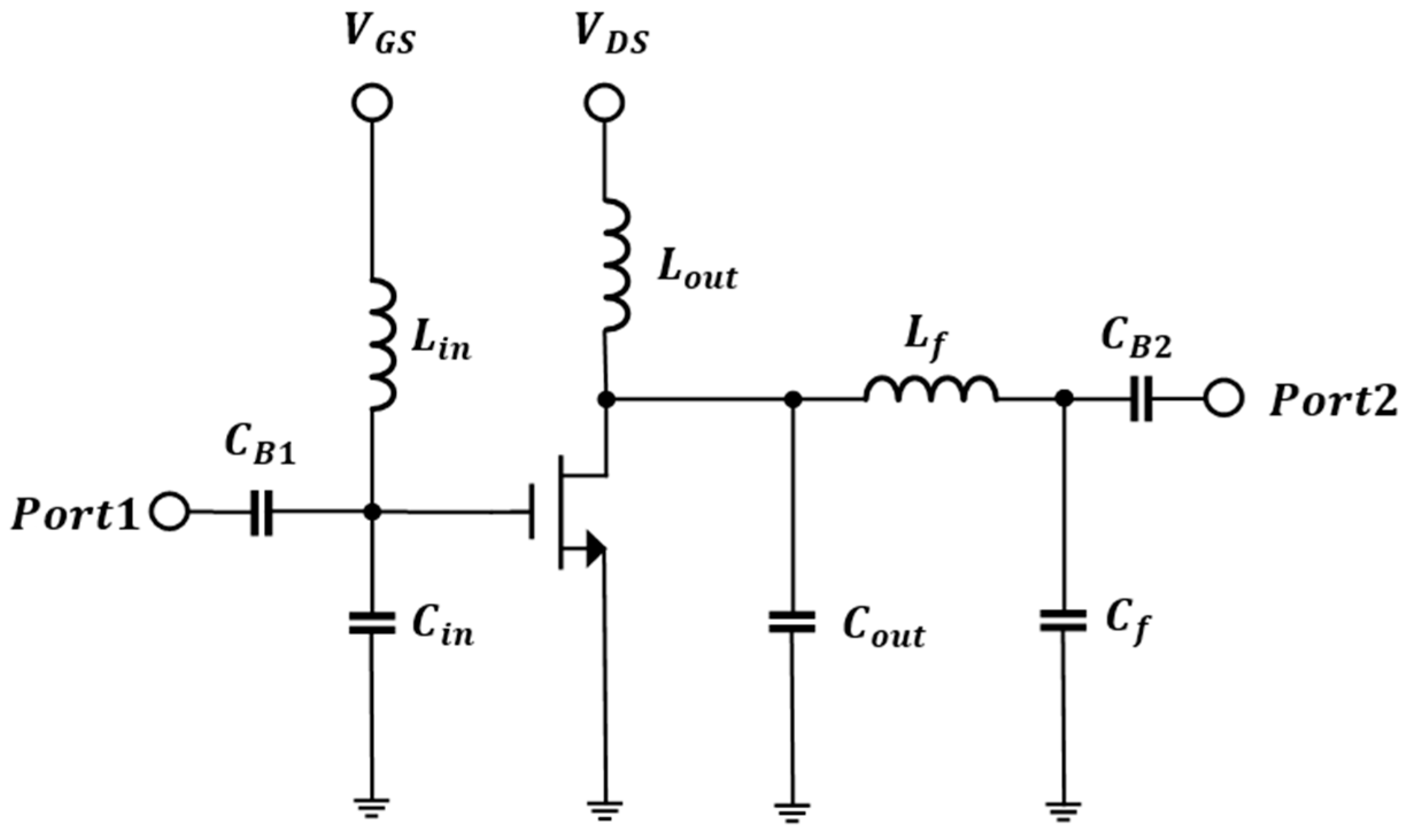
The output matching circuit in the class-E PA converts the low-output impedance at the drain of the switching transistor to the reference impedance and reduces the harmonics at the output. The configuration of the matching circuit that uses a large number of components is advantageous to achieve the desired characteristics. However, there is a problem, in that the performance can be changed owing to the variation of the values of the components. The L-type matching circuit is useful at the output of the PA in the wireless power transfer system because it can implement the output matching with the use of the minimum number of components at a narrow frequency bandwidth [10,13]. Figure 1 shows the circuit diagram of a class-E PA with an L-type matching network using a series inductor Lf and a shunt capacitor Cf. The switching transistor is used as the LDMOS transistor, which can operate with low on-resistance at high frequency. The drain-source voltage (VDS) should be higher than 30 V to obtain an output power Pout in excess of 100 W when the output resistance Ro at the drain is assumed to be 5 Ω. From the VDS and the class-E operation [17], the transistor should also have a breakdown voltage VBV of 110 V, or higher, as follows
The capacitors CB1 and CB2 are used for blocking DC voltages from the input and output ports. The input matching of the amplifier is designed using a shunt inductor Lin and a shunt capacitor Cin, considering the input capacitance of the switching transistor at the bias point. Class-E operation at 6.78 MHz is realized by using a high-Q inductor Lout and an additional CDS capacitor Cout connected at the drain node of the transistor. The current of the high-Q inductor should be considered in the design by the maximum current in the class-E mode.
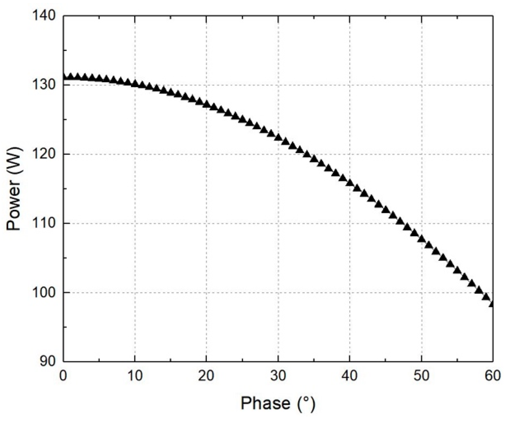
The simulated Pout and PAE of the schematic design are shown in Figure 2 when the semiconductors from the LDMOS transistor, MRFE6VP6300HR3, manufactured by NXP, are used as a switching device. The input power of the PA is set to be 21 dBm, and the gate and drain biases are designed to be 1.9 V and 36 V for the class-E operation of the amplifier, respectively. The output of the power transmitter in the system must be matched with the reference impedance of 50 Ω because the input impedance of the transmission coil of the wireless power transfer system is typically designed to be the reference impedance [18]. The power dissipation of the amplifier matched at the reference load impedance of 50 Ω is simulated to be equal to 18.9 W owing to the Pout of 97.2 W and the PAE of 83.7%. The maximum PAE can be obtained at the load impedance of 31 Ω from the simulation results, but the Pout of 67.5 W at the impedance is not enough to achieve the output power of 100 W or more. From the simulation results at the load impedance of 31 Ω, it can be expected that the output power will yield a power in excess of 100 W by combining the Pout of the two PAs. The maximum PAE and the output power in excess of 100 W can be achieved using the two PAs with directly connected to the optimum load impedance of 15.5 Ω, as shown in Figure 3. However, the losses and the generated heat can be increased by the inductors used in the matching circuit of the two directly-connected PAs, because the high-powered signal at the load is transmitted to the circuit. Since the conventional power combiner has input and output impedances that are matched with the reference impedance, impedance matching circuits are required between the PAs. The latter are designed at the optimum load impedance of 31 Ω for obtaining the maximum PAE with the power combiner, as shown in Figure 4. The matching circuits in Figure 4 are not with the L-type network in Figure 1 because the network is included in the amplifier itself to reduce the harmonics. Correspondingly, the output characteristics of the PA with the maximum PAE at 31 Ω are shown at port 2 of Figure 1. It is generally difficult to determine which configuration can yield a higher efficiency in the overall transmitting module because the output performances can be degraded even further by the generated heat of the high-powered single PA, and by the additional loss at the power combiner, and the mismatch of the combined dual PAs. Therefore, the circuit configuration of the power module should be determined to obtain an output power that is greater than 100 W and a higher PAE in the transmitter, thus allowing the comparison between the high-powered single PA and the combined dual PAs.
2.2. Proposed Power Module with an Adaptive Power Combiner
The most common power combiner is the Wilkinson power combiner that consists of two quarter-wavelength transmission lines and a resistor with an impedance that is twice the reference impedance located between the two input ports [19]. A quarter-wavelength transmission line in the power combiner at 6.78 MHz can be implemented by substituting with the π-network with the lumped elements using one inductor, with a value of L1, and two capacitors, with the values of C1, as shown in Figure 5a, because of its long physical length on the PCB. The inductance L1 and the capacitance C1 in the power combiner can be obtained as
where Ro is the reference impedance of 50 Ω, and ω is the angular frequency of the combiner that is equal to 2π × 6.78 MHz. Inductors, with a high quality (Q) factor > 100, are used in the combiner to prevent efficiency degradation owing to the losses in the inductors [10]. There is no impedance conversion in the conventional combiner because the input and output ports are matched to the reference impedance. Thus, additional matching circuits are essential when the PAs are operated at the load impedance with the maximum PAE, as shown in Figure 4. The use of the matching circuits increases additional losses relevant to the overall transmission efficiency, especially when the inductors are used in the circuits. It can be expected that the efficiency of the power combiner in Figure 4 is generally lower than that of the single PA if the efficiency of the PA itself is not greatly improved by changing the load conditions.
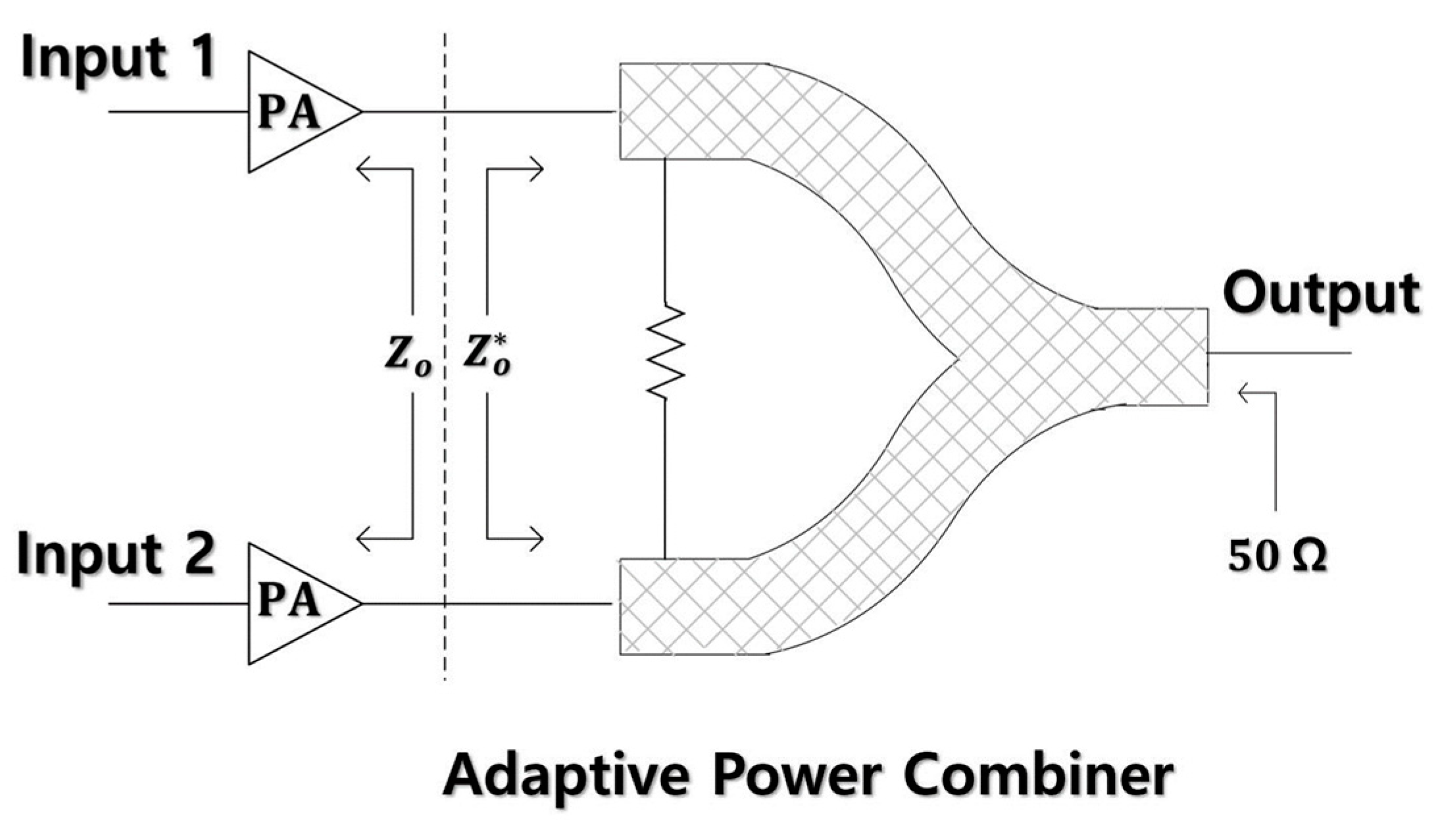
An adaptive power combiner is proposed, as shown in Figure 5b, to combine the outputs of PAs operating at the load conditions that maximize the PAE, without using the additional matching circuits. For impedance matching with the outputs of PAs, the combiner can realize an adaptive input matching by arranging the resistance R1 and the capacitors C2 between two input ports in series. The output impedance matching of the combiner is implemented in both the power combiners using the inductors with the value of L1 and the capacitors with the value of C1. There is an intrinsic loss in the combiner due to the inductors with the values of L1. This loss is not different from that of the conventional combiner because it can be perceived as the loss of the power combiner itself. The additional loss of the proposed combiner can be neglected since both of combiners use the same inductance L1 in Figure 5. The proposed power combiner can improve the efficiency of the power module by merging the impedance matching and power combining without additional matching circuits, as shown in Figure 6.
The proposed power combiner used for increasing the overall transmission efficiency of the power module is used for its design. It can transmit an output power of more than 100 W at 6.78 MHz, as shown in Figure 7. Two power amplifiers in the proposed module are identically designed to obtain the maximum PAE at 31 Ω as shown in Figure 2. Additionally, DC blocking capacitors between the amplifiers and the combiner are removed, while the capacitor Cf in the L-type network of the PA and the capacitor C1 in the combiner can be merged to a single capacitor with the value of C1 + Cf since they share the same node connection. The power module for the same bias conditions achieved an output power of 106 W and a PAE of 88.6% in the circuit simulation. Compared with the single PA, the output power and the PAE increased by 9 W and 4.9%, respectively. The performance improvement is perceived to be caused by the optimization of the impedance matching between the PA and the adaptive power combiner in the proposed module. The impedance matching at the output of the power module was decreased by 4.3 dB, but the output matching of −9.7 dB was enough for its use as the transmitter in the wireless power transfer system. The proposed power module yielded a higher output power and PAE compared to the single class-E PA as shown in Table 1, which summarizes the simulation results of the single PA and the proposed module using the dual PAs.
2.3. Electromagnetic Field and Radio Frequency Circuit Co-Simulation
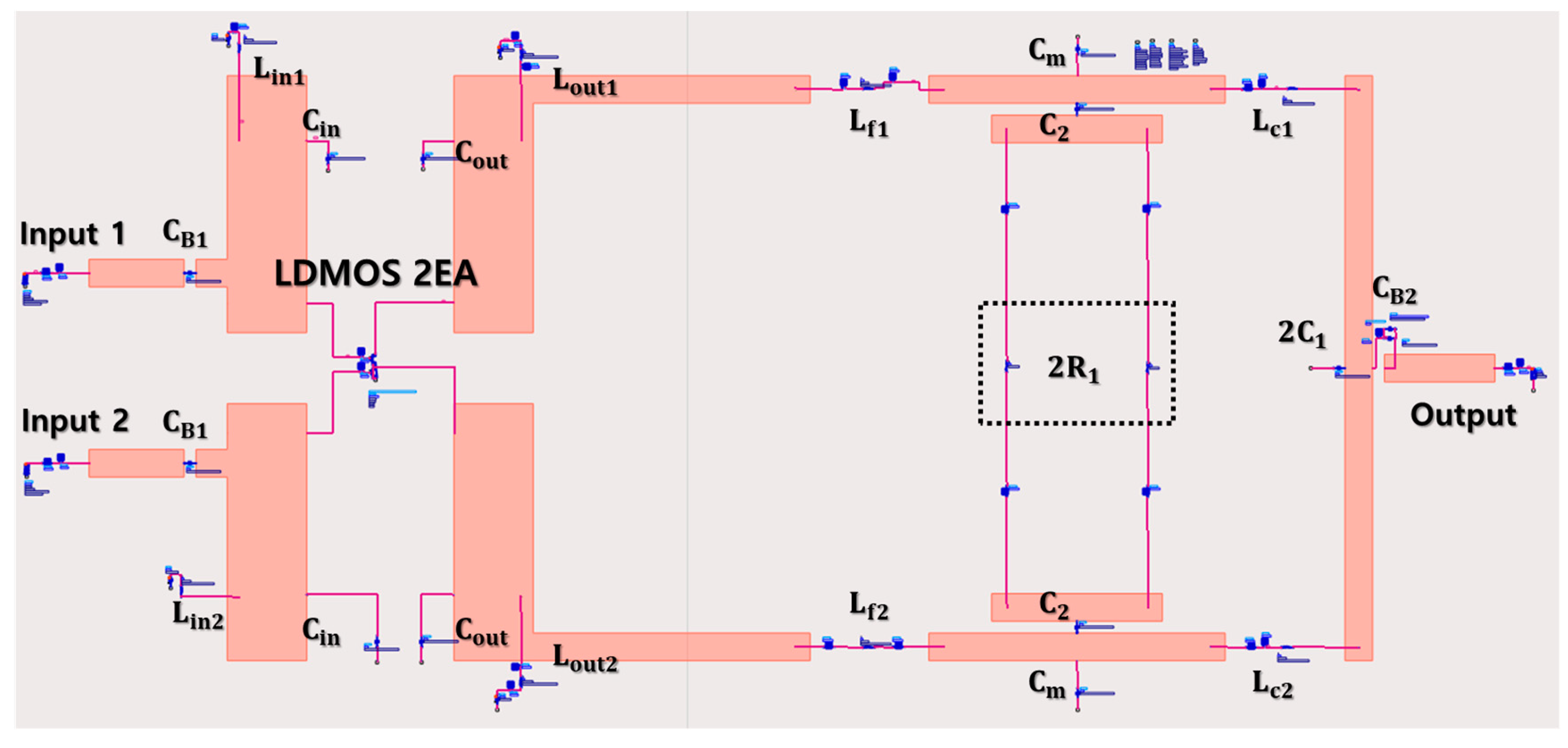
The proposed power module may elicit an increased degradation in its measurement performance, owing to the parasitic components that are generated in its implementation compared to the single PA. This is because the module has an additional PA and a combiner compared to a high-power PA. A co-simulation method that employed both an EM field and an RF circuit was used to compare the performances between the single PA and the proposed module. This included the parasitic effects in the implementations of the PA, and the module on the FR4 PCBs [12]. The characteristics of the transmission lines required to implement the power module on the PCB were simulated by using the Keysight Advanced Design System (ADS) Momentum, and the co-simulation in Figure 8 was conducted by applying the device models provided by the manufacturers in a similar manner to the case of the circuit simulation. The landing patterns used to attach the inductors and capacitors were designed by considering the solderable area and the size of each component. The resistor R1 located between the two inputs of the combiner was configured in parallel to the high-powered ceramic resistors with values of 250 Ω and 82 Ω for obtaining an accurate design value. The capacitors C1 and Cf were combined into a single capacitor with the value of Cm, which is the sum of C1 and Cf, for the sake of simplicity. The design parameters are summarized in Table 2.
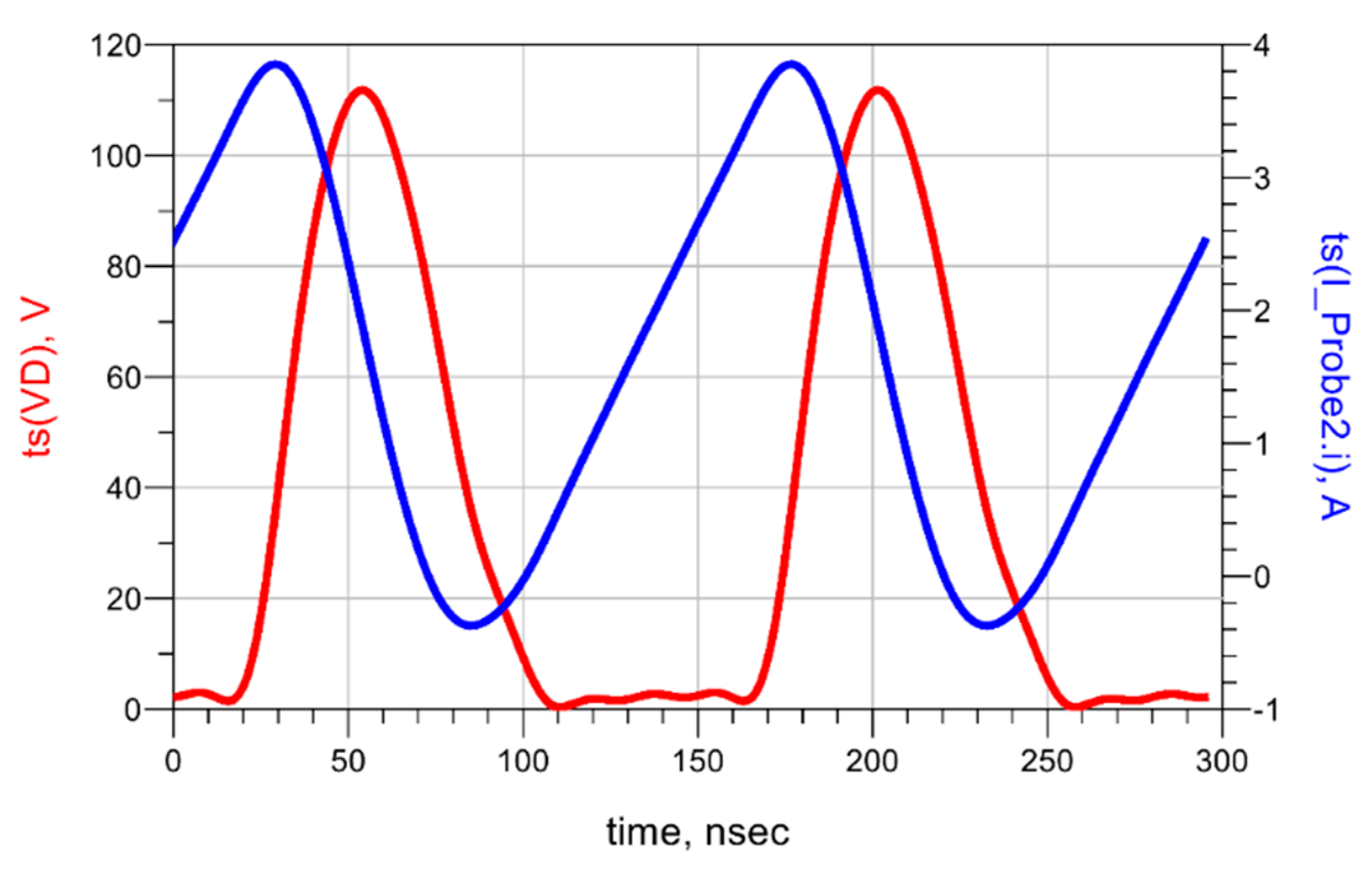
Figure 9 shows the transient voltage current waveforms of the PA in the module, and the class- E operation can be observed from the voltage waveforms at the drain node of the transistor and the current waveforms passing through the inductor Lout. The proposed module yielded an output power of 104.7 W and a PAE of 88.5% at 6.78 MHz in the co-simulation when the drain voltage of 36 V and the gate voltage of 1.9 V were applied to each amplifier of the module. The co-simulation results showed the degradation of the 2.2 W output power and the 0.1% PAE compared to the circuit simulation results, but they still yielded a 6.8 W greater output power and a 4.8% higher PAE than the output performances of the single PA in Table 1.
3. Results
3.1. Implementation of the Proposed Power Module
The proposed power module was implemented on the FR4 PCB, with a thickness of 1 mm as shown in Figure 10. Two PAs are symmetrically designed using the LDMOS device with two transistors in one package. Therefore, the characteristic difference caused by the mismatch in the pattern and interconnection between the two PAs can be minimized. The heat sink consists of an aluminum metal body with a thickness of 15 mm and a cooling fan with the diameter of 10 mm. It is attached on the ground layer of the PCB for preventing performance degradation owing to the generated heat in the LDMOS transistors and the toroidal inductors. Capacitors, with a breakdown voltage of 250 V and inductors, with the maximum available current of 4.2 A, are used in the module to prevent the destruction and degradation caused by the voltage swing of class-E operation and the current flow of the high-power transmission, respectively. The size of the fabricated module is 94.7 mm × 62.5 mm without the subminiature version A (SMA) connectors.
3.2. Measurement Results
Figure 11 shows the measurement setup for obtaining the output power and PAE of the proposed power module. A 6.78 MHz signal, with a power of 25.3 dBm from the signal generator, is transmitted to each input of the class-E PA by the power divider, which is manufactured by Mini-Circuits. The input driving power of each PA is 22.2 dBm, considering the loss of 3.1 dBm resulted from the S-parameter measurement of the power divider. Because the output power of the proposed module exceeds the maximum input power of the spectrum analyzer, the output power of the module is measured after the signal was passed through a 50-dB attenuator constructed by RF-Lambda. The output power is calibrated using the signal loss induced by the RF cables and interconnection mismatches. The gate and drain voltages of the two PAs are connected to each other and supplied using a DC power supply. The PAE of the proposed power module is calculated using the input power displayed on the signal generator, the output power displayed on the calibrated spectrum analyzer, the drain voltage set by the DC power supply, and the total current consumption supplied to the module [13]. The maximum drain voltage in the measurement is set to be 41 V based on Equation (1) and the breakdown voltage of the LDMOS transistor.
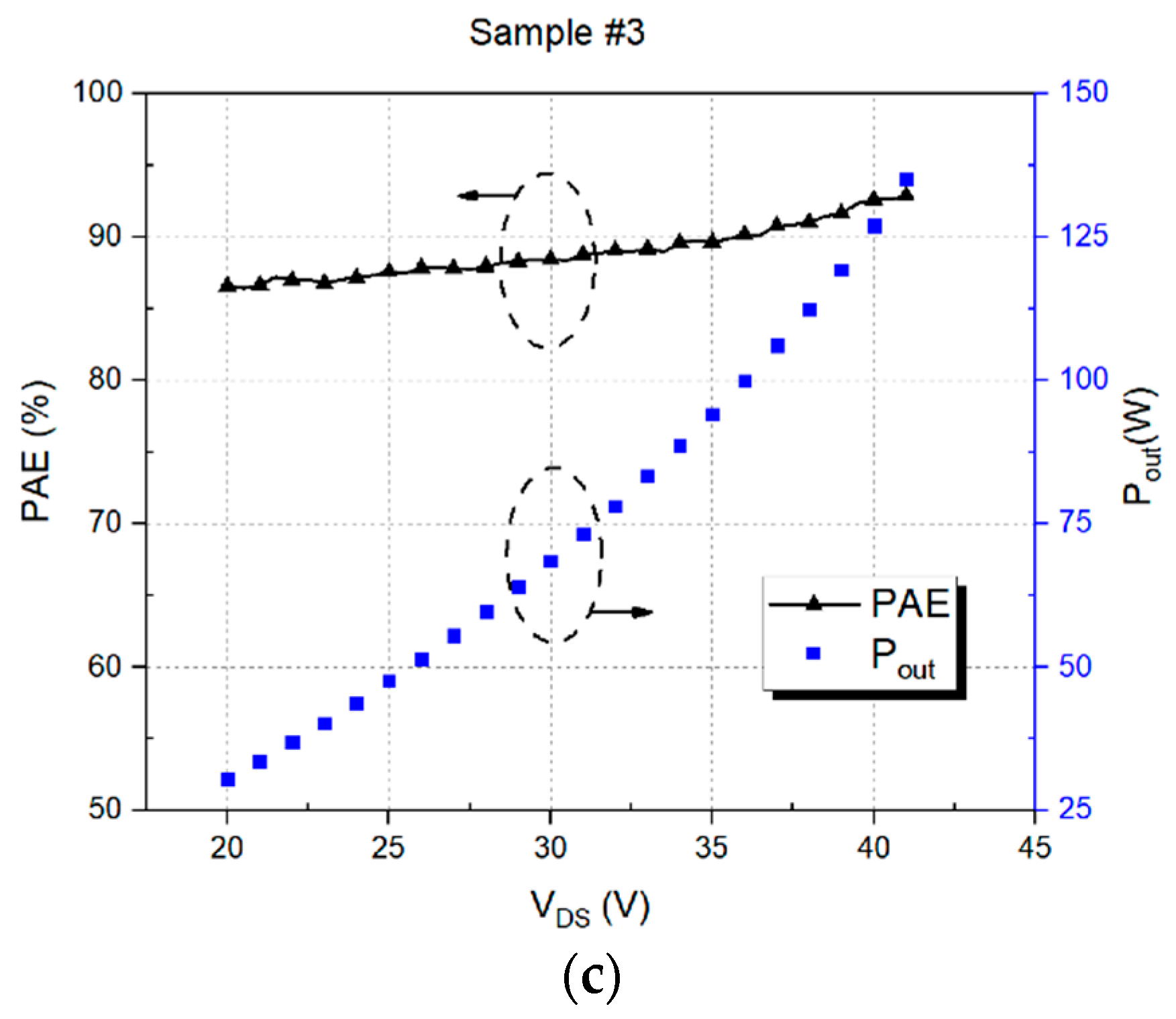
Because of the tolerance of the components, it is difficult in the implementation to use inductors that perfectly meet the designed inductances based on the simulation and the devices that exactly have the same value in the design of the two PAs. Three power modules are measured, as shown in Figure 12, to confirm whether the output performances of the proposed module can be stably represented when the different values from the design parameters are used in the implementation. All three power modules yielded output powers that were higher than 100 W, and PAEs of above 89.7% when the gate and drain voltages of the power module were biased to 2.2 V and 36 V in the measurements, respectively. The maximum output power and the best PAE in the bias conditions were 102.1 W for sample #1 and 90.4% for sample #2, respectively. The measurement results of the proposed module were approximately similar to the co-simulation results, and the existing minor differences are perceived to be caused by changes in the gate voltage in the measurements.
Most of the remaining power that is not used for power transmission and amplification is generally converted to heat. Extreme heat generation can cause a decrease in the output performances and lower the stability of the transmitter. The performance degradation and instability due to heat generation are particularly important in the transmitter of the wireless power transfer system because a long operating time is required for charging the devices. The output power and PAE after operating for one hour are measured, as shown in Figure 13, to verify whether the output performances of the proposed module are degraded by the heat generated in the module. The measured output power and PAE of the module are obtained to be equal to 123.3 W and 85.7% at the bias conditions with the gate and drain voltages of 2.2 V and 41 V, respectively. The measured performances in the same bias conditions as the measurement in Figure 12 are decreased by 4.3 W and 4.0%, respectively. However, no phenomena exhibiting unstable operation, such as oscillation, frequency shifting, or fluctuation in the output signals of the module, are observed in the measurement.
It is necessary to verify the harmonic signals at the output of the transmitter because the second harmonic of the power module can directly affect the operation of the near-field communication (NFC) system at 13.56 MHz. The proposed power module can reduce the harmonics at the output because a low-pass filter using the L-type network is implemented at the output of each class-E PA in the module. As shown in Figure 14, the second and third harmonics are measured to be −37.8 dBc and −63 dBc, respectively, as compared to the fundamental signal. The harmonic signal at the output of the module is obtained to be more than 13 dBm due to the high-output power that is greater than 50 dBm. However, the effect of the harmonics on the surroundings can be further reduced in the wireless power transfer system because the transmitting and receiving coils of the system operate as a bandpass filter at 6.78 MHz [14].
4. Discussion
Although the values of the inductors used in the three samples were slightly different as shown in Table 3, the deviations at the output in the measurement results were not large. The total resistance from the node for supplying the drain voltage to the output in each module can be calculated from the Q factors of the used inductors, as shown in Table 4. Because the total resistance by the inductors present in sample #1 are smaller than those in sample #3, the higher PAE in sample #3 compared to sample #1 cannot be explained by the outcomes of the previous study, which is that the Q factor of the inductor is one of the dominant factors to decrease the PAE [10]. Therefore, a new analysis is required to explain the performance variation of the output power and PAE obtained in the measurements in each module.
The characteristic mismatch of the two PAs in the proposed module is the other factor that can affect the performance variations among the power modules. In the proposed power module, the components of the PAs can be modeled as signals with different magnitudes and phases that are applied to the inputs of the power combiner. When the outputs of each of the two PAs in the module are defined to be PTX1 and PTX2, the combining efficiency η in the power combiner can be described using the ratio of the perfectly combining power and the mismatched power, as follows
where |ATX1| and |ATX2| are the amplitudes of the output signals PTX1 and PTX2, respectively, and θ is the phase difference between the two output signals. When the square of the difference in the amplitude between the two signals can be neglected due to the small difference in the amplitude, (5) can be approximately expressed as
The efficiency in the power combiner decreases as the phase difference between the two signals increases. Additionally, the change in the efficiency depends on the characteristics of the cosine function. The symmetry of the PAs can be evaluated by the ratio of the AC current from each power supply because the load impedance conditions depend on the drain-source current IDS when the DC bias from the supply is fixed. The amplitudes of the AC current consumed by each PA of sample #1 and sample #3 were measured after one hour of operation of the power module, with a power supply of 36 V. The amplitude ratio in each PA obtained in sample #3 was compared to that of sample #1. The symmetry obtained from the amplitude ratio in sample #3 was calculated to be equal to 87.5%, which was higher than 85.7% of that in sample #1. Based on the amplitude ratio of the AC currents of the two PAs in the module, the measurements in Figure 11 can be accepted as the result of the fact that the symmetry of the two PAs of sample #3 was higher than those of sample #1.
Figure 15 shows the results of the co-simulation in the adaptive power combiner. Two 6.78 MHz signals with a different phase are input to the power combiner in the simulation. The output power of two signals is set to 70 W, which is the power level at the load condition necessary to obtain the maximum PAE using the given LDMOS transistor. The simulation results show that the output power can be decreased by 6.7%, which is the power combining loss of 8.8 W when a phase difference of 30 degrees occurs at the input. Since the difference in the components of the power combiner can affect the output characteristics in the same manner as the phase difference, it is also an important factor in the proposed power module in obtaining the symmetry of the two-signal path in the combiner [20].
5. Conclusions
A 120 W power module is proposed for a 6.78 MHz wireless power transfer system with increased transmission efficiency. The proposed power module consisted of two class-E PAs symmetrically designed at the optimum load condition and of an adaptive power combiner that stably obtained an increased combining efficiency. The power combiner used discrete components implements the desired impedance using capacitors and resistors between the two inputs of the combiner for impedance matching with the load condition, to obtain the maximum PAE in the PA. The symmetry between the PAs can affect the output performances of the proposed module because of the unique architectural feature of the use of the two PAs. The EM field and RF circuit co-simulation, which accounted for the parasitic effects on a PCB, showed that the proposed module had a higher output power and PAE than a single high-powered PA at 6.78 MHz. The measurement results of the three power modules implemented using different components demonstrated that the proposed power module can obtain stable and constant output performances, regardless of the changes in these components.
Author Contributions
J.-R.Y. identified the framework of this study and defined the research theme. U.-G.C. designed the proposed power module and performed the measurements. All authors analyzed the measured data, wrote the original draft, and edited the manuscript.
Acknowledgments
This work was funded by the 2017 Yeungnam University Research Grant No. 217A580039. And this work was also supported by the Basic Science Research Program through the National Research Foundation of Korea (NRF) funded by the Ministry of Science, ICT and Future Planning (grant number 2017R1C1B2002285).
Conflicts of Interest
The authors declare no conflict of interest.
References
- André, K.; Karalis, A.; Moffatt, R.; Joannopoulos, J.D.; Fisher, P.; Soljai, M. Wireless power transfer via strongly coupled magnetic resonances. Science 2007, 317, 83–86. [Google Scholar]
- Inventions & Experiments of Nikola Tesla. Available online: https://teslaresearch.jimdo.com/wireless-transmission-of-energy-1/ (accessed on 16 June 2018).
- Aqeel, M.J.; Rosdiadee, N.; Sadik, K.G.; Haider, M.J.; Mahamod, I. Opportunities and Challenges for Near-Field Wireless Power Transfer: A Review. Energies 2017, 10, 1022. [Google Scholar]
- Riehl, P.S.; Satyamoorthy, A.; Akram, H.; Yen, Y.C.; Yang, J.C.; Juan, B.; Philip, F.T. Wireless power systems for mobile devices supporting inductive and resonant operating modes. IEEE. Trans. Microw. Theory Tech. 2015, 63, 780–790. [Google Scholar] [CrossRef]
- Kim, C.G.; Seo, D.H.; You, J.S.; Park, J.H.; Cho, B.H. Design of a contactless battery charger for cellular phone. IEEE Trans. Ind. Electron. 2001, 48, 1238–1247. [Google Scholar]
- The 60 Watt Specification. Available online: https://www.wirelesspowerconsortium.com/developers/60-watt-applications.html (accessed on 10 June 2018).
- Zenkner, H.; Khan-Ngern, W. Low loss magnetic design for wireless power transfer. Adv. Sci. Lett. 2015, 21, 2967–2973. [Google Scholar] [CrossRef]
- Mukti, R.J.; Begum, N.P.; Islam, A. Analysis of medium range wireless power transfer system using magnetic resonant coupling. In Proceedings of the International Conference on Informatics, Electronics & Vision, Dhaka, Bangladesh, 23–24 May 2014. [Google Scholar]
- Nair, V.V.; Choi, J.R. An efficiency enhancement technique for a wireless power transmission system based on a multiple coil switching technique. Energies 2016, 9, 156. [Google Scholar] [CrossRef]
- Yang, J.R.; Kim, J.; Park, Y.J. Class E power amplifiers using high-Q inductors for loosely coupled wireless power transfer system. J. Electr. Eng. Technol. 2014, 9, 569–575. [Google Scholar] [CrossRef]
- Cannon, B.L.; Hoburg, J.F.; Stancil, D.D.; Goldstein, S.C. Magnetic resonant coupling as a potential means for wireless power transfer to multiple small receivers. IEEE Trans. Power Electron. 2009, 24, 1819–1825. [Google Scholar] [CrossRef]
- Yang, J.-R. A class E power oscillator for 6.78-MHz wireless power transfer system. J. Electr. Eng. Technol. 2018, 13, 220–225. [Google Scholar]
- Grebennikov, A.V. Switched-mode rf and microwave parallel circuit class E power amplifiers. Int. J. RF Microw. Comput.-Aided Eng. 2004, 14, 21–35. [Google Scholar] [CrossRef]
- Yang, J.-R.; Son, H.-C.; Park, Y.-J. A class E power amplifier with coupling coils for a wireless power transfer system. Prog. Electromagn. Res. C 2013, 35, 13–22. [Google Scholar] [CrossRef]
- Chou, H.L.; Ng, J.C.W.; Liou, R.H.; Jong, Y.C.; Tuan, H.C.; Huang, C.F. The effect of self-heating in ldmosfet expansion regime. IEEE Trans. Electron Dev. 2012, 59, 3042–3047. [Google Scholar] [CrossRef]
- Choi, U.-G.; Yang, J.-R. A 6.78-MHz 100-W class E power amplifier module with an adaptive power combiner. In Proceedings of the IEEE International Symposium on Radio-Frequency Integration Technology, Melbourne, Australia, 15–17 August 2018. [Google Scholar]
- Grebennikov, A.; Sokal, N.O. Switchmode RF Power Amplifiers; Elsevier: Oxford, UK, 2007; ISBN 978-0-7506-7962-6. Available online: https://www.sciencedirect.com/science/book/9780750679626#book-description (accessed on 31 July 2018).
- Duong, T.P.; Lee, J.-W. A Dynamically adaptable impedance-matching system for midrange wireless power transfer with misalignment. Energies 2015, 8, 7593–7617. [Google Scholar] [CrossRef]
- Pozar, D.M. Microwave Engineering, 4th ed.; John Wiley Sons: Hoboken, NJ, USA, 2011; ISBN 978-0-470-63155-3. Available online: https://www.wiley.com/en-us/Microwave+Engineering%2C+4th+Edition-p-9780470631553 (accessed on 31 July 2018).
- Eccleston, K.W. Efficiency of lossless power combiners. Microw. Opt. Technol. Lett. 1995, 10, 9–12. [Google Scholar] [CrossRef]
Figure 1.
Schematic of a class-E power amplifier using an L-type matching network at the output stage.
Figure 1.
Schematic of a class-E power amplifier using an L-type matching network at the output stage.

Figure 2.
Simulation results of the class-E power amplifier in Figure 1 depending on the load impedance at the output.
Figure 2.
Simulation results of the class-E power amplifier in Figure 1 depending on the load impedance at the output.

Figure 3.
Two class-E power amplifiers connected with the optimum load impedance Zo: (a) Block diagram of the amplifiers; (b) simulation results of the two PAs with the direct connection to the optimum load.
Figure 3.
Two class-E power amplifiers connected with the optimum load impedance Zo: (a) Block diagram of the amplifiers; (b) simulation results of the two PAs with the direct connection to the optimum load.
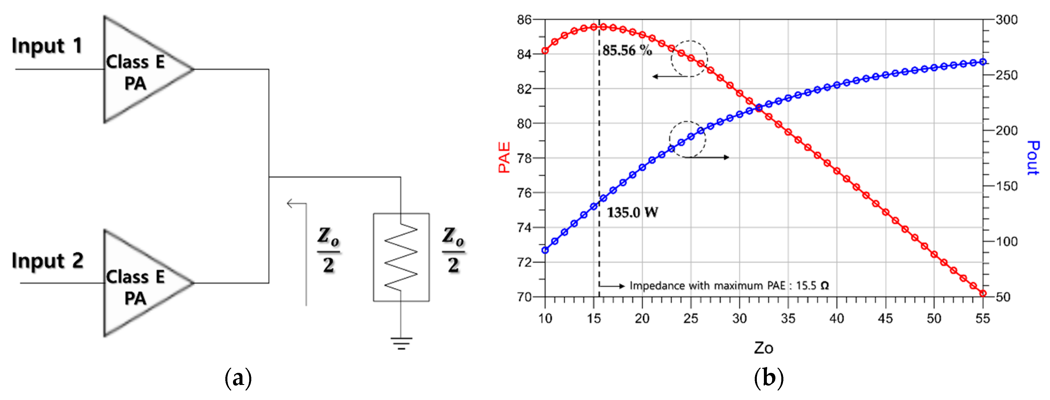
Figure 4.
Conventional power-combining configuration for impedance matching between the power amplifiers and the power combiner.
Figure 4.
Conventional power-combining configuration for impedance matching between the power amplifiers and the power combiner.
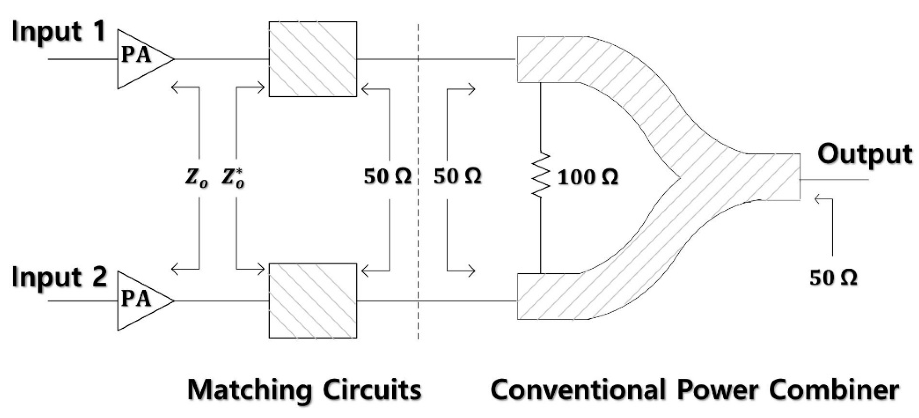
Figure 5.
Schematic of the power combiner using lumped elements: (a) Conventional power combiner with the matched input and output ports; (b) proposed power combiner with the input ports matched to the outputs of the PAs and the output port matched to the reference impedance.
Figure 5.
Schematic of the power combiner using lumped elements: (a) Conventional power combiner with the matched input and output ports; (b) proposed power combiner with the input ports matched to the outputs of the PAs and the output port matched to the reference impedance.
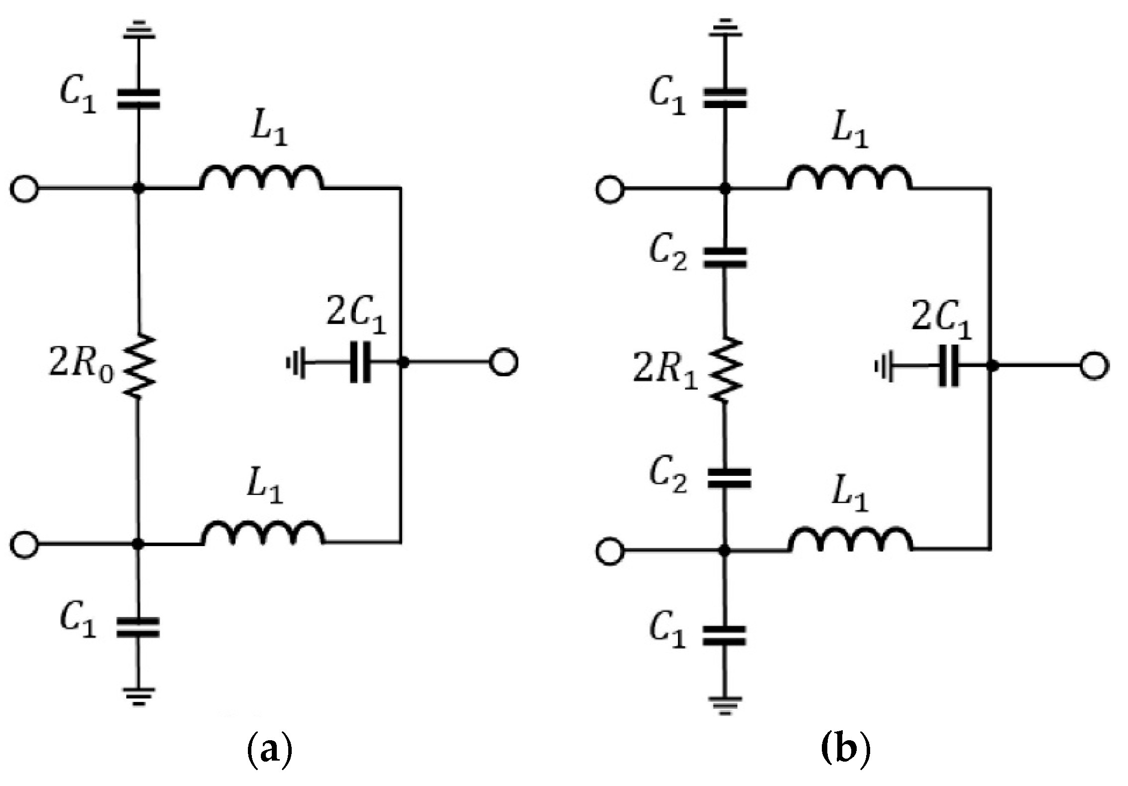
Figure 6.
Proposed power module using two power amplifiers and an adaptive power combiner (Re(Zo) = Re(Zo*) = 31 Ω).
Figure 6.
Proposed power module using two power amplifiers and an adaptive power combiner (Re(Zo) = Re(Zo*) = 31 Ω).

Figure 7.
Schematic of the proposed power amplifier module with the adaptive power combiner.
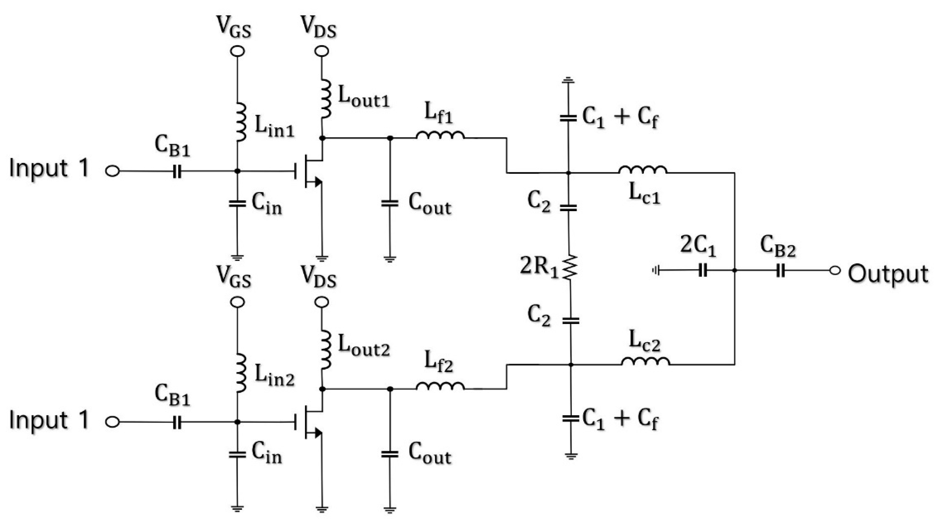
Figure 8.
Electromagnetic (EM) field and radio frequency (RF) circuit co-simulation of the proposed power module including the effects of the layout design on FR4 PCB.
Figure 8.
Electromagnetic (EM) field and radio frequency (RF) circuit co-simulation of the proposed power module including the effects of the layout design on FR4 PCB.

Figure 9.
Transient waveforms using the EM field and RF circuit co-simulation at the drain node of the transistor.
Figure 9.
Transient waveforms using the EM field and RF circuit co-simulation at the drain node of the transistor.

Figure 10.
Photograph of the fabricated power module on FR4 PCB.
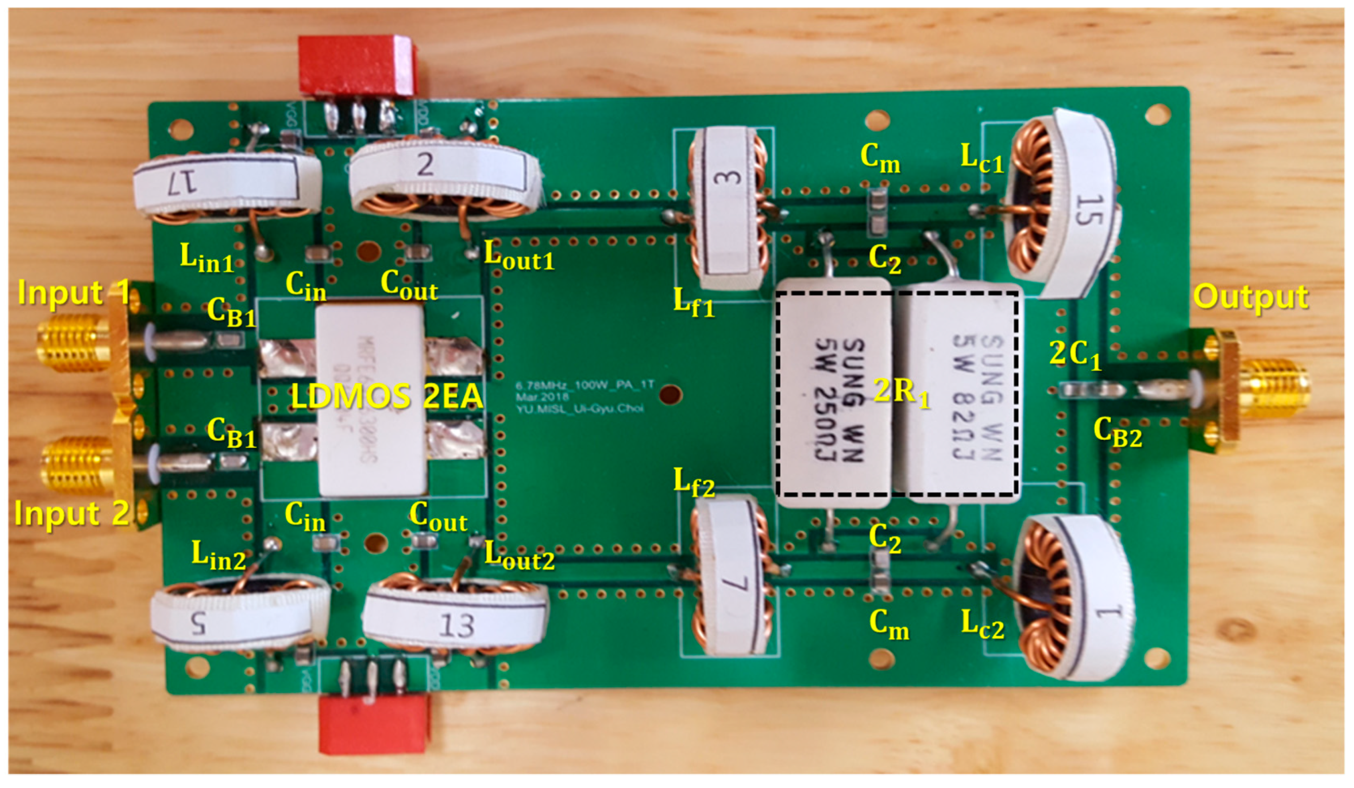
Figure 11.
Measurement setup for obtaining the output power and calculating the PAE of the proposed power module.
Figure 11.
Measurement setup for obtaining the output power and calculating the PAE of the proposed power module.
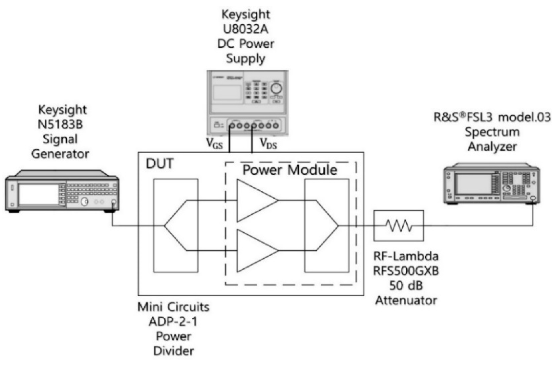
Figure 12.
Measurements of the output power and PAE of the proposed power module: (a) Sample #1; (b) sample #2; and (c) sample #3.
Figure 12.
Measurements of the output power and PAE of the proposed power module: (a) Sample #1; (b) sample #2; and (c) sample #3.
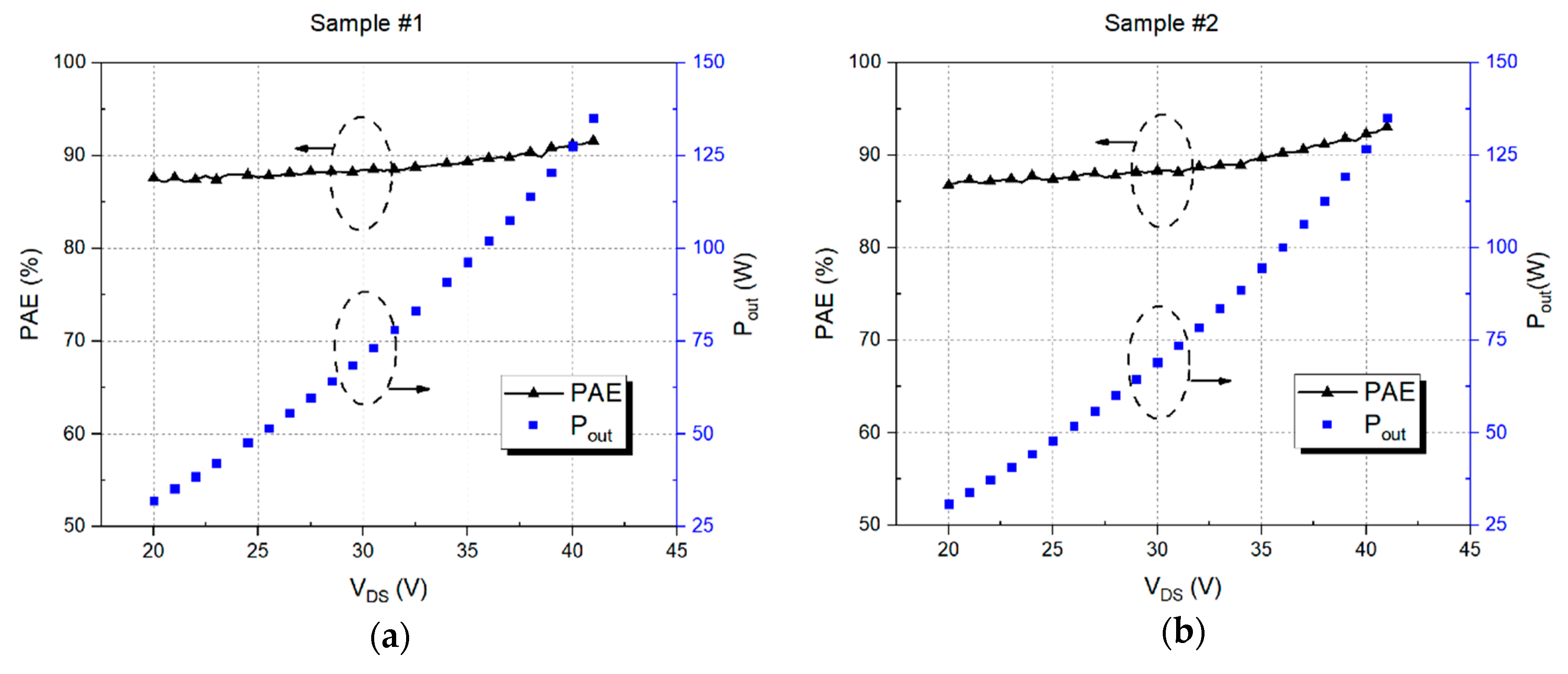

Figure 13.
Measured results of the proposed power module after operation for a period of one hour.
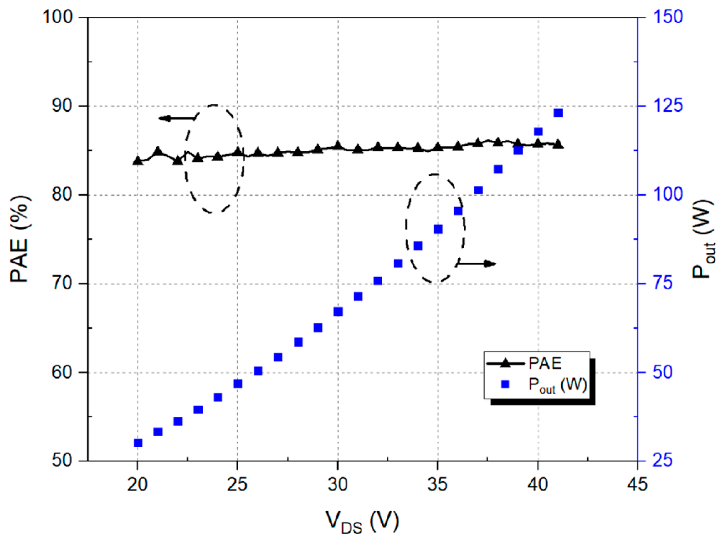
Figure 14.
Output spectrum of the proposed power module.
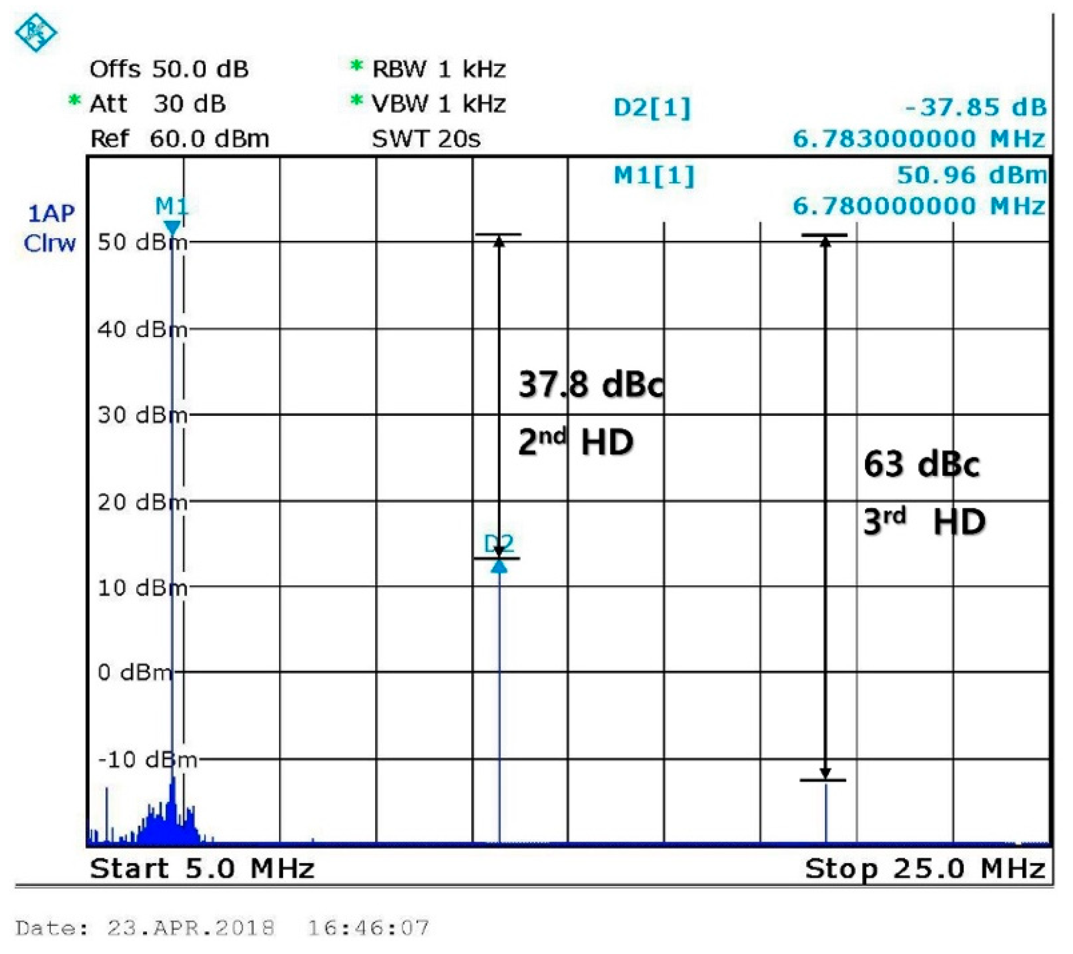
Figure 15.
Simulated output power depending on the phase difference of the two input signals of the adaptive power combiner.
Figure 15.
Simulated output power depending on the phase difference of the two input signals of the adaptive power combiner.

Table 1.
Comparisons of the performances of the single class-E power amplifier (PA), and the proposed power module using the dual PAs in the schematic simulation.
Table 1.
Comparisons of the performances of the single class-E power amplifier (PA), and the proposed power module using the dual PAs in the schematic simulation.
| Output Power (W) | Power-Added Efficiency (PAE) (%) | Input Return Loss (dB) | Output Return Loss (dB) | |
|---|---|---|---|---|
| Single PA | 97.2 | 83.7 | 15.2 | 14.0 |
| Dual PAs | 106.2 | 88.6 | 15.3 | 9.7 |
| Difference | 9.0 | 4.9 | 0.1 | −4.3 |
| Components | Value | Components | Value |
|---|---|---|---|
| 2R1 | 62 Ω | CB2 | 20 nF |
| Lin | 305 nH | Cin | 1500 pF |
| Lout | 640 nH | Co | 820 pF |
| Lf | 650 nH | Cm (= C1 + Cf) | 1500 pF |
| Lc1 | 1170 nH | C2 | 120 pF |
| CB1 | 270 pF | 2C1 | 1200 pF |
Table 3.
Inductances and quality factors of the inductors used in the fabricated power modules.
| Components | Sample #1 | Sample #2 | Sample #3 | |||
|---|---|---|---|---|---|---|
| Inductance [nH] | Q Factor | Inductance [nH] | Q Factor | Inductance [nH] | Q Factor | |
| Lin1 | 307 | 110 | 306 | 107 | 304 | 117 |
| Lin2 | 307 | 110 | 306 | 104 | 304 | 114 |
| Lout1 | 648 | 149 | 649 | 148 | 649 | 140 |
| Lout2 | 648 | 147 | 649 | 155 | 649 | 139 |
| Lf1 | 647 | 141 | 647 | 146 | 647 | 133 |
| Lf2 | 647 | 157 | 647 | 148 | 646 | 138 |
| Lc1 | 1177 | 107 | 1179 | 110 | 1176 | 108 |
| Lc2 | 1177 | 107 | 1179 | 107 | 1176 | 109 |
Table 4.
Calculated total resistance using the Q factors by inductors from the node for supplying the drain voltage to the output in each module.
Table 4.
Calculated total resistance using the Q factors by inductors from the node for supplying the drain voltage to the output in each module.
| Path to the output | Sample #1 [mΩ] | Sample #2 [mΩ] | Sample #3 [mΩ] |
|---|---|---|---|
| From PA 1 | 849.4 | 832.2 | 868.6 |
| From PA 2 | 852.0 | 834.0 | 857.9 |
| Total Resistance | 1701.4 | 1666.2 | 1726.5 |
© 2018 by the authors. Licensee MDPI, Basel, Switzerland. This article is an open access article distributed under the terms and conditions of the Creative Commons Attribution (CC BY) license (http://creativecommons.org/licenses/by/4.0/).
Share and Cite
MDPI and ACS Style
Choi, U.-G.; Yang, J.-R. A 120 W Class-E Power Module with an Adaptive Power Combiner for a 6.78 MHz Wireless Power Transfer System. Energies 2018, 11, 2083. https://doi.org/10.3390/en11082083
AMA Style
Choi U-G, Yang J-R. A 120 W Class-E Power Module with an Adaptive Power Combiner for a 6.78 MHz Wireless Power Transfer System. Energies. 2018; 11(8):2083. https://doi.org/10.3390/en11082083
Chicago/Turabian StyleChoi, Ui-Gyu, and Jong-Ryul Yang. 2018. "A 120 W Class-E Power Module with an Adaptive Power Combiner for a 6.78 MHz Wireless Power Transfer System" Energies 11, no. 8: 2083. https://doi.org/10.3390/en11082083
Note that from the first issue of 2016, this journal uses article numbers instead of page numbers. See further details here.